Tag Archives: Jae-Hwang Lee

Tough colour and the flower beetle

The flower beetle Torynorrhina flammea. [downloaded from https://www.nanowerk.com/nanotechnology-news2/newsid=58269.php]

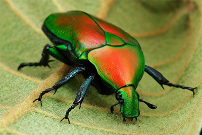
That is one gorgeous beetle and a June 17, 2021 news item on Nanowerk reveals that it features in a structural colour story (i.e, how structures rather than pigments create colour),

The unique mechanical and optical properties found in the exoskeleton of a humble Asian beetle has the potential to offer a fascinating new insight into how to develop new, effective bio-inspired technologies.

Pioneering new research by a team of international scientists, including Professor Pete Vukusic from the University of Exeter, has revealed a distinctive, and previously unknown property within the carapace of the flower beetle – a member of the scarab beetle family.

The study showed that the beetle has small micropillars within the carapace – or the upper section of the exoskeleton – that give the insect both strength and flexibility to withstand damage very effectively.

Crucially, these micropillars are incorporated into highly regular layering in the exoskeleton that concurrently give the beetle an intensely bright metallic colour appearance.

A June 18, 2021 University of Exeter press release (also on EurekAlert but published June 17, 2021), delves further into the researchers’ new insights,

For this new study, the scientists used sophisticated modelling techniques to determine which of the two functions – very high mechanical strength or conspicuously bright colour – were more important to the survival of the beetle.

They found that although these micropillars do create a highly enhanced toughness of the beetle shell, they were most beneficial for optimising the scattering of coloured light that generates its conspicuous appearance.

The research is published this week in the leading journal, Proceedings of the National Academy of Sciences, PNAS.

Professor Vukusic, one of three leads of the research along with Professor Li at Virginia Tech and Professor Kolle at MIT [Massachusetts Institute of Technology], said: “The astonishing insights generated by this research have only been possible through close collaborative work between Virginia Tech, MIT, Harvard and Exeter, in labs that trailblaze the fields of materials, mechanics and optics. Our follow-up venture to make use of these bio-inspired principles will be an even more exciting journey.”.

The seeds of the pioneering research were sown more than 16 years ago as part of a short project created by Professor Vukusic in the Exeter undergraduate Physics labs. Those early tests and measurements, made by enthusiastic undergraduate students, revealed the possibility of intriguing multifunctionality.

The original students examined the form and structure of beetles’ carapce to try to understand the simple origin of their colour. They noticed for the first time, however, the presence of strength-inducing micropillars.

Professor Vukusic ultimately carried these initial findings to collaborators Professor Ling Li at Virginia Tech and Professor Mathias Kolle at Harvard and then MIT who specialise in the materials sciences and applied optics. Using much more sophisticated measurement and modelling techniques, the combined research team were also to confirm the unique role played by the micropillars in enhancing the beetles’ strength and toughness without compromising its intense metallic colour.

The results from the study could also help inspire a new generation of bio-inspired materials, as well as the more traditional evolutionary research.

By understanding which of the functions provides the greater benefit to these beetles, scientists can develop new techniques to replicate and reproduce the exoskeleton structure, while ensuring that it has brilliant colour appearance with highly effective strength and toughness.

Professor Vukusic added: “Such natural systems as these never fail to impress with the way in which they perform, be it optical, mechanical or in another area of function. The way in which their optical or mechanical properties appear highly tolerant of all manner of imperfections too, continues to offer lessons to us about scientific and technological avenues we absolutely should explore. There is exciting science ahead of us on this journey.”

Here’s a link to and a citation for the paper,

Microstructural design for mechanical–optical multifunctionality in the exoskeleton of the flower beetle Torynorrhina flammea by Zian Jia, Matheus C. Fernandes, Zhifei Deng, Ting Yang, Qiuting Zhang, Alfie Lethbridge, Jie Yin, Jae-Hwang Lee, Lin Han, James C. Weaver, Katia Bertoldi, Joanna Aizenberg, Mathias Kolle, Pete Vukusic, and Ling Li. PNAS June 22, 2021 118 (25) e2101017118; DOI: https://doi.org/10.1073/pnas.2101017118

This paper is behind a paywall.

Better RRAM memory devices in the short term

Given my recent spate of posts about computing and the future of the chip (list to follow at the end of this post), this Rice University [Texas, US] research suggests that some improvements to current memory devices might be coming to the market in the near future. From a July 12, 2014 news item on Azonano,

Rice University’s breakthrough silicon oxide technology for high-density, next-generation computer memory is one step closer to mass production, thanks to a refinement that will allow manufacturers to fabricate devices at room temperature with conventional production methods.

A July 10, 2014 Rice University news release, which originated the news item, provides more detail,

Tour and colleagues began work on their breakthrough RRAM technology more than five years ago. The basic concept behind resistive memory devices is the insertion of a dielectric material — one that won’t normally conduct electricity — between two wires. When a sufficiently high voltage is applied across the wires, a narrow conduction path can be formed through the dielectric material.

The presence or absence of these conduction pathways can be used to represent the binary 1s and 0s of digital data. Research with a number of dielectric materials over the past decade has shown that such conduction pathways can be formed, broken and reformed thousands of times, which means RRAM can be used as the basis of rewritable random-access memory.

RRAM is under development worldwide and expected to supplant flash memory technology in the marketplace within a few years because it is faster than flash and can pack far more information into less space. For example, manufacturers have announced plans for RRAM prototype chips that will be capable of storing about one terabyte of data on a device the size of a postage stamp — more than 50 times the data density of current flash memory technology.

The key ingredient of Rice’s RRAM is its dielectric component, silicon oxide. Silicon is the most abundant element on Earth and the basic ingredient in conventional microchips. Microelectronics fabrication technologies based on silicon are widespread and easily understood, but until the 2010 discovery of conductive filament pathways in silicon oxide in Tour’s lab, the material wasn’t considered an option for RRAM.

Since then, Tour’s team has raced to further develop its RRAM and even used it for exotic new devices like transparent flexible memory chips. At the same time, the researchers also conducted countless tests to compare the performance of silicon oxide memories with competing dielectric RRAM technologies.

“Our technology is the only one that satisfies every market requirement, both from a production and a performance standpoint, for nonvolatile memory,” Tour said. “It can be manufactured at room temperature, has an extremely low forming voltage, high on-off ratio, low power consumption, nine-bit capacity per cell, exceptional switching speeds and excellent cycling endurance.”

In the latest study, a team headed by lead author and Rice postdoctoral researcher Gunuk Wang showed that using a porous version of silicon oxide could dramatically improve Rice’s RRAM in several ways. First, the porous material reduced the forming voltage — the power needed to form conduction pathways — to less than two volts, a 13-fold improvement over the team’s previous best and a number that stacks up against competing RRAM technologies. In addition, the porous silicon oxide also allowed Tour’s team to eliminate the need for a “device edge structure.”

“That means we can take a sheet of porous silicon oxide and just drop down electrodes without having to fabricate edges,” Tour said. “When we made our initial announcement about silicon oxide in 2010, one of the first questions I got from industry was whether we could do this without fabricating edges. At the time we could not, but the change to porous silicon oxide finally allows us to do that.”

Wang said, “We also demonstrated that the porous silicon oxide material increased the endurance cycles more than 100 times as compared with previous nonporous silicon oxide memories. Finally, the porous silicon oxide material has a capacity of up to nine bits per cell that is highest number among oxide-based memories, and the multiple capacity is unaffected by high temperatures.”

Tour said the latest developments with porous silicon oxide — reduced forming voltage, elimination of need for edge fabrication, excellent endurance cycling and multi-bit capacity — are extremely appealing to memory companies.

“This is a major accomplishment, and we’ve already been approached by companies interested in licensing this new technology,” he said.

Here’s a link to and a citation for the paper,

Nanoporous Silicon Oxide Memory by Gunuk Wang, Yang Yang, Jae-Hwang Lee, Vera Abramova, Huilong Fei, Gedeng Ruan, Edwin L. Thomas, and James M. Tour. Nano Lett., Article ASAP DOI: 10.1021/nl501803s Publication Date (Web): July 3, 2014

Copyright © 2014 American Chemical Society

This paper is behind a paywall.

As for my recent spate of posts on computers and chips, there’s a July 11, 2014 posting about IBM, a 7nm chip, and much more; a July 9, 2014 posting about Intel and its 14nm low-power chip processing and plans for a 10nm chip; and, finally, a June 26, 2014 posting about HP Labs and its plans for memristive-based computing and their project dubbed ‘The Machine’.