On the heels of yesterday’s(Sept. 26, 2013) posting about carbon nnanotubes as flexible gas sensors, I have this item about a computer fashioned from carbon nanotubes.

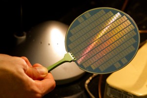
This wafer contains tiny computers using carbon nanotubes, a material that could lead to smaller, more energy-efficient processors. Courtesy Stanford University
To me this looks more like a ping pong bat than a computer wafer. Regardless, here’s more about it from a Sept. 25, 2013 news item by James Morgan for BBC (British Broadcasting Corporation) News online,
The first computer built entirely with carbon nanotubes has been unveiled, opening the door to a new generation of digital devices.
“Cedric” is only a basic prototype but could be developed into a machine which is smaller, faster and more efficient than today’s silicon models.
Nanotubes have long been touted as the heir to silicon’s throne, but building a working computer has proven awkward.
…
Cedric is the most complex carbon-based electronic system yet realised.So is it fast? Not at all. It might have been in 1955.
The computer operates on just one bit of information, and can only count to 32.“In human terms, Cedric can count on his hands and sort the alphabet. But he is, in the full sense of the word, a computer,” says co-author [of the paper published in Nature] Max Shulaker.
Tom Abate’s Sept. 26, 2013 article for Stanford Report provides more detail about carbon nanotubes, their potential for replacing silicon chips and associated problems,
“Carbon nanotubes [CNTs] have long been considered as a potential successor to the silicon transistor,” said Professor Jan Rabaey, a world expert on electronic circuits and systems at the University of California-Berkeley.
…
Why worry about a successor to silicon?
Such concerns arise from the demands that designers place upon semiconductors and their fundamental workhorse unit, those on-off switches known as transistors.
For decades, progress in electronics has meant shrinking the size of each transistor to pack more transistors on a chip. But as transistors become tinier, they waste more power and generate more heat – all in a smaller and smaller space, as evidenced by the warmth emanating from the bottom of a laptop.
Many researchers believe that this power-wasting phenomenon could spell the end of Moore’s Law, named for Intel Corp. co-founder Gordon Moore, who predicted in 1965 that the density of transistors would double roughly every two years, leading to smaller, faster and, as it turned out, cheaper electronics.
But smaller, faster and cheaper has also meant smaller, faster and hotter.
…
“CNTs could take us at least an order of magnitude in performance beyond where you can project silicon could take us,” Wong [another co-author of the paper] said.
But inherent imperfections have stood in the way of putting this promising material to practical use.
First, CNTs do not necessarily grow in neat parallel lines, as chipmakers would like.
Over time, researchers have devised tricks to grow 99.5 percent of CNTs in straight lines. But with billions of nanotubes on a chip, even a tiny degree of misaligned tubes could cause errors, so that problem remained.
A second type of imperfection has also stymied CNT technology.
Depending on how the CNTs grow, a fraction of these carbon nanotubes can end up behaving like metallic wires that always conduct electricity, instead of acting like semiconductors that can be switched off.
Since mass production is the eventual goal, researchers had to find ways to deal with misaligned and/or metallic CNTs without having to hunt for them like needles in a haystack.
“We needed a way to design circuits without having to look for imperfections or even know where they were,” Mitra said.
The researchers have dubbed their solution an “imperfection-immune design,” from the Abate article,
To eliminate the wire-like or metallic nanotubes, the Stanford team switched off all the good CNTs. Then they pumped the semiconductor circuit full of electricity. All of that electricity concentrated in the metallic nanotubes, which grew so hot that they burned up and literally vaporized into tiny puffs of carbon dioxide. This sophisticated technique eliminated the metallic CNTs in the circuit.
Bypassing the misaligned nanotubes required even greater subtlety.
The Stanford researchers created a powerful algorithm that maps out a circuit layout that is guaranteed to work no matter whether or where CNTs might be askew.
“This ‘imperfections-immune design’ [technique] makes this discovery truly exemplary,” said Sankar Basu, a program director at the National Science Foundation.
The Stanford team used this imperfection-immune design to assemble a basic computer with 178 transistors, a limit imposed by the fact that they used the university’s chip-making facilities rather than an industrial fabrication process.
Their CNT computer performed tasks such as counting and number sorting. It runs a basic operating system that allows it to swap between these processes. In a demonstration of its potential, the researchers also showed that the CNT computer could run MIPS, a commercial instruction set developed in the early 1980s by then Stanford engineering professor and now university President John Hennessy.
Though it could take years to mature, the Stanford approach points toward the possibility of industrial-scale production of carbon nanotube semiconductors, according to Naresh Shanbhag, a professor at the University of Illinois at Urbana-Champaign and director of SONIC, a consortium of next-generation chip design research.
Here’s a link to and a citation for the paper,
Carbon nanotube computer by Max M. Shulaker, Gage Hills, Nishant Patil, Hai Wei, Hong-Yu Chen, H.-S. Philip Wong, & Subhasish Mitra. Nature 501, 526–530 (26 September 2013) doi:10.1038/nature12502
This article is behind a paywall but you can gain temporary access via ReadCube.
