Tag Archives: Purdue University

$14.5M to take nanoHUB to the ‘next level’

According to the Feb. 5, 2013 news item on Nanotechnology Now, nanoHUB , online science and engineering gateway based at Purdue University, Indiana, is going to be receiving a $14.5M five year grant from the US National Science Foundation (NSF),

“Thousands of times a day the leading researchers ‘come’ to Purdue through the globally unique tool of nanoHUB,” Purdue President Mitch Daniels said Tuesday (Feb. 5) in announcing the grant. “The new NSF investment is an affirmation of the brilliance of nanoHUB’s Purdue creators and of its worldwide scientific significance.”

Annually, nearly 250,000 users in 172 countries participate in nanoHUB, an online meeting place for simulation, research, collaboration, teaching, learning and publishing. The nanoHUB provides a library of 267 simulation tools, free from the limitations of running software locally, used in the scientific computing cloud by more than 12,000 people every year.

The Internet-based initiative provides 3,000 resources from more than 1,000 authors for research and education in the areas of nanoelectronics and nanoelectromechanical systems and their application to nano-biosystems. The nanoHUB menu also includes courses, tutorials, seminars, discussions and facilities to foster nano-research collaboration, including the Birck Nanotechnology Center in Purdue’s Discovery Park.

The Purdue University Feb. 5, 2013 news release, which originated the news item, provides more details although some are a bit confusing (Note: Links have been removed),

The Purdue-led Cyber Platform, a part of the Network for Computational Nanotechnology (NCN), will assist researchers across the globe by developing a virtual society that shares simulation software, data and other innovative content to provide engineers and scientists with the fundamental knowledge required to advance nanoscience into nanotechnology.

Through Cyber Platform developments and community engagement efforts, the nanoHUB in its next phase is designed to:

* Accelerate research by transforming nanoscience to nanotechnology through the integration of simulation with experimental data.

* Inspire and educate the next-generation nanoscience and nanotechnology workforce.

* Expand the nanoHUB society that uses and shares content on the Web-based portal.

“Our long-term vision for the Cyber Platform is to use the nanoHUB as an online nano society that researchers, practitioners, educators and students depend on daily,” said Purdue electrical and computer engineering professor Gerhard Klimeck, principal investigator of the Purdue-led Cyber Platform. “At the same time, we are excited about how this tool has extended into professional practice as a computational resource for a multidisciplinary culture of innovation grounded in cloud services-enabled workflows.”

The NSF award abstract helps to clear up matters,

Network for Computational Nanotechnology (NCN) was founded in 2002 to advance nanoscience toward nanotechnology via online simulations on nanoHUB.org. Not only has nanoHUB become the first broadly successful, scientific end-to-end cloud computing environment, but it also has evolved well beyond online simulation. Annually, nanoHUB provides a library of 3,000 learning resources to 195,000 users worldwide. Its 232 simulation tools, free from the limitations of running software locally, are used in the cloud by over 10,800 annually. Its impact is demonstrated by 720+ citations to nanoHUB in the scientific literature with over 4,807 secondary citations, yielding an h-index of 31, and by a median time from publication of a research simulation program to classroom use of less than 6 months. Cumulatively, over 14,000 students in over 760 formal classes in over 100 institutions have used nanoHUB simulations.

Despite a decade of transformational success for a broad nanotechnology research and education community, significant gaps remain as work is still performed by isolated individuals and small groups. This fragmentation by specialty hinders tool and data sharing across knowledge domains. Nano areas such as bio, photonics, and materials are only beginning to use nanoHUB while manufacturing, informatics, environmental-health-and-safety are to date not even represented on nanoHUB. The NCN Cyber Platform proposes to address these gaps through efforts in three strategic goals to: 1) accelerate research by transforming nanoscience to nanotechnology through the integration of simulation with experimentation; 2) inspire and educate the next-generation nanoscience and nanotechnology workforce; and 3) grow the nanoHUB society that uses and shares nanoHUB content. Five cross-cutting thrust areas focus on the cyberinfrastructure (CI) and social dynamics of the nanoHUB virtual society: CI innovation; content stewardship and node engagement; education research and precollege/college and lifelong learning; outreach, diversity, and marketing; and CI operations. The 10-year NCN nanoHUB Cyber Platform vision is that nanoHUB will be the online nano society that researchers, practitioners, educators and students depend on day-to-day while simultaneously immersed in professional practice and computational resources for a multidisciplinary culture of innovation grounded in cloud services-enabled workflows.

Intellectual Merit: The NCN nanoHUB strategic plan will answer two fundamental challenges to the next-generation nanoHUB experience: 1) development of technologies that enable simple management and publication of scientific data (experimental and simulation) without additional complex steps: and 2) the establishment of a value system that fosters publication of data, tools, and lectures similar to today’s rewards for journal publications. CI innovation, developed through the leading HUBzero platform as well as in cooperation with other CI efforts, will enable new connection points for research, education, and commercialization, expanded platform tool features to help users exchange and publish data; combined data and tools for verification, validation, and engineering activities; and increase immersive and pervasive features. Through partnerships with professional societies and commercial publishers, nanoHUB will change how researchers publish their simulation results through novel interactive journals that reflect a user’s workflow, link directly back to their data, and make the work reproducible. This value system will drive new content toward nanoHUB, obviating the need for content generation to be monetarily supported by NCN. Through partnerships with the three new NCN content nodes and other NSF-funded nano efforts, NCN will continue to foster content creation to demonstrate value to the authors and will prototype, test, and host the proposed new technologies for broad usage.

Broader Impacts: NCN has developed processes that enabled researchers to rapidly deploy their research codes and innovative tutorials and classes on nanoHUB. To date, these processes harvested research and educational results from 890 contributors world-wide. Expansion into new areas of nano research and education, including pre-college education, represent a huge growth potential for nanoHUB that goes beyond simulation to embracing data management, search, and exploration. Focus on diversity will continue to be an integral part of NCN’s outreach program, in particular through focused workshops and new initiatives such as EPICS High. The NCN-pioneered HUBzero already powers 40 HUBs at 12 institutions, serving a broad range of science and engineering disciplines and commercialization. Through impact assessment and continual contributions to HUBzero software stack releases, nanoHUB will continue to drive impact beyond its nano society into other disciplines and institutions.

While this duplicates some of the text in the NSF award abstract, it does offer some new nuggests, from the Purdue University news release,

The nanoHUB has become the first broadly successful, cloud-computing environment for research across multiple disciplines, with more than 960 citations in scientific literature and 8,000 secondary citations, with nearly one-third of those papers involving experimental data. It also has evolved well beyond online simulation for research.

From New York to London and Moscow to Madrid, more than 14,000 students in 760 formal classes at 185 institutions have used nanoHUB simulations for classroom teaching, homework and projects. The nanoHUB also provides a library of 3,000 learning materials.

“Most of these tools are adopted for formal education in six months, compared with the 3.8 years it takes for the release of new college textbook editions,” Klimeck said.

NCN founding director Mark Lundstrom, the Don and Carol Scifres Distinguished Professor of Electrical and Computer Engineering at Purdue, said a key part of the Cyber Platform project is to engage an ever-larger and more diverse cyber community that shares novel, high-quality nanoscale computation and simulation research and educational resources.

“The reason we created the nanoHUB cyberinfrastructure 10 years ago was to connect those who are doing simulation with experimental collaborators,” Lundstrom said. “Today, it’s called cloud computing.”

Here’s a for those who want to check out the Network for Computational Nanotechnology (NCN.  For another history of nanoHUB, check my Nov. 6, 2010 posting and for the little bit I have on HUBzero, there’s my Feb. 20, 2012 posting about the session concerning that platform at the American Association for the Advancement of Science (AAAS) 2012 annual meeting.

Christmas-tree shaped ‘4-D’ nanowires

This Dec. 5, 2012 news item on Nanowerk features a seasonal approach to a study about ‘4-D’ nanowires,

A new type of transistor shaped like a Christmas tree has arrived just in time for the holidays, but the prototype won’t be nestled under the tree along with the other gifts.

“It’s a preview of things to come in the semiconductor industry,” said Peide “Peter” Ye, a professor of electrical and computer engineering at Purdue University.

Researchers from Purdue and Harvard universities created the transistor, which is made from a material that could replace silicon within a decade. Each transistor contains three tiny nanowires made not of silicon, like conventional transistors, but from a material called indium-gallium-arsenide. The three nanowires are progressively smaller, yielding a tapered cross section resembling a Christmas tree.

Sadly, Purdue University (Indiana, US) will not be releasing any images to accompany their Dec. 4, 2012 news release (which originated the news item) about the ‘4-D’ transistor  until Saturday, Dec. 8, 2012.  So here’s an image of a real Christmas tree from the National Christmas Tree Organization’s Common Tree Characteristics webpage,

Douglas Fir Christmas tree from http://www.realchristmastrees.org/dnn/AllAboutTrees/TreeCharacteristics.aspx


The Purdue University news release written by Emil Venere provides more detail about the work,

“A one-story house can hold so many people, but more floors, more people, and it’s the same thing with transistors,” Ye said. “Stacking them results in more current and much faster operation for high-speed computing. This adds a whole new dimension, so I call them 4-D.”

The work is led by Purdue doctoral student Jiangjiang Gu and Harvard postdoctoral researcher Xinwei Wang.

The newest generation of silicon computer chips, introduced this year, contain transistors having a vertical 3-D structure instead of a conventional flat design. However, because silicon has a limited “electron mobility” – how fast electrons flow – other materials will likely be needed soon to continue advancing transistors with this 3-D approach, Ye said.

Indium-gallium-arsenide is among several promising semiconductors being studied to replace silicon. Such semiconductors are called III-V materials because they combine elements from the third and fifth groups of the periodic table.

Transistors contain critical components called gates, which enable the devices to switch on and off and to direct the flow of electrical current. Smaller gates make faster operation possible. In today’s 3-D silicon transistors, the length of these gates is about 22 nanometers, or billionths of a meter.

The 3-D design is critical because gate lengths of 22 nanometers and smaller do not work well in a flat transistor architecture. Engineers are working to develop transistors that use even smaller gate lengths; 14 nanometers are expected by 2015, and 10 nanometers by 2018.

However, size reductions beyond 10 nanometers and additional performance improvements are likely not possible using silicon, meaning new materials will be needed to continue progress, Ye said.

Creating smaller transistors also will require finding a new type of insulating, or “dielectric” layer that allows the gate to switch off. As gate lengths shrink smaller than 14 nanometers, the dielectric used in conventional transistors fails to perform properly and is said to “leak” electrical charge when the transistor is turned off.

Nanowires in the new transistors are coated with a different type of composite insulator, a 4-nanometer-thick layer of lanthanum aluminate with an ultrathin, half-nanometer layer of aluminum oxide. The new ultrathin dielectric allowed researchers to create transistors made of indium-gallium- arsenide with 20-nanometer gates, which is a milestone, Ye said.

This work will be presented at the 2012 International Electron Devices (IEEE [Institute of Electrical and Electronics Engineers]) meeting in San Francisco, California, Dec. 10 – 12, 2012 (as per the information on the registration page) with the two papers written by the team will be published in the proceedings.

I have a full list of the authors, from the news release,

The authors of the research papers are Gu [Jiangjiang Gu]; Wang [Xinwei Wang]; Purdue doctoral student H. Wu; Purdue postdoctoral research associate J. Shao; Purdue doctoral student A. T. Neal; Michael J. Manfra, Purdue’s William F. and Patty J. Miller Associate Professor of Physics; Roy Gordon, Harvard’s Thomas D. Cabot Professor of Chemistry; and Ye [Peide “Peter” Ye].

Eeek! The sticky tape is coming after us!

Fingers emerged from sticky tape to form claws in a research project conducted at Purdue University (Indiana, US), which will be presented at a meeting of the Materials Research Society (MRS) in Boston from Sunday (Nov. 25) to Nov. 30, 2012. The Nov. 20, 2012 news release on EurekAlert describes the new ‘smart’ material,

Researchers used a laser to form slender half-centimeter-long fingers out of the tape. When exposed to water, the four wispy fingers morph into a tiny robotic claw that captures water droplets.

The innovation could be used to collect water samples for environmental testing, said Babak Ziaie, a Purdue University professor of electrical and computer engineering and biomedical engineering.

“It  [the tape] can be micromachined into different shapes and works as an inexpensive smart material that interacts with its environment to perform specific functions,” he said.

Doctoral student Manuel Ochoa came up with the idea. While using tape to collect pollen, he noticed that it curled when exposed to humidity. The cellulose-acetate absorbs water, but the adhesive film repels water.

“So, when one side absorbs water it expands, the other side stays the same, causing it to curl,” Ziaie said.

A laser was used to machine the tape to a tenth of its original thickness, enhancing this curling action. The researchers coated the graspers with magnetic nanoparticles so that they could be collected with a magnet.

“Say you were sampling for certain bacteria in water,” Ziaie said. “You could drop a bunch of these and then come the next day and collect them.”

Sticky tape is one of  my favourite pieces of science equipment along with inkjet printers and ‘Shrinky Dinks’ as I noted in my Nov. 16, 2012 posting about bio-ink. The Nov. 20, 2012 news release by Emil Venere can also be found on the Purdue University website along with photos and other materials such as this animated GIF of the gripper closing available at https://engineering.purdue.edu/ZBML/img/research/plain-gripper-closing.gif.

Blood, tears, and urine for use in diagnostic tools

Frankly, I’d rather just spit into a cup or onto a slide for diagnostic tests than having to supply urine or have my blood drawn. I don’t think that day has arrived yet but scientists at Purdue University (Indiana, US) have made a breakthrough. From the Aug. 23, 2012 news item on ScienceDaily,

Researchers have created a new type of biosensor that can detect minute concentrations of glucose in saliva, tears and urine and might be manufactured at low cost because it does not require many processing steps to produce.

“It’s an inherently non-invasive way to estimate glucose content in the body,” said Jonathan Claussen, a former Purdue University doctoral student and now a research scientist at the U.S. Naval Research Laboratory. “Because it can detect glucose in the saliva and tears, it’s a platform that might eventually help to eliminate or reduce the frequency of using pinpricks for diabetes testing. We are proving its functionality.”

Claussen and Purdue doctoral student Anurag Kumar led the project, working with Timothy Fisher, a Purdue professor of mechanical engineering; D. Marshall Porterfield, a professor of agricultural and biological engineering; and other researchers at the university’s Birck Nanotechnology Center.

The originating Aug. 20, 2012 Purdue University news release by Emil Venere provides details as to how this biosensor works,

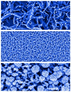
The sensor has three main parts: layers of nanosheets resembling tiny rose petals made of a material called graphene, which is a single-atom-thick film of carbon; platinum nanoparticles; and the enzyme glucose oxidase.

Each petal contains a few layers of stacked graphene. The edges of the petals have dangling, incomplete chemical bonds, defects where platinum nanoparticles can attach. Electrodes are formed by combining the nanosheet petals and platinum nanoparticles. Then the glucose oxidase attaches to the platinum nanoparticles. The enzyme converts glucose to peroxide, which generates a signal on the electrode.

“Typically, when you want to make a nanostructured biosensor you have to use a lot of processing steps before you reach the final biosensor product,” Kumar said. “That involves lithography, chemical processing, etching and other steps. The good thing about these petals is that they can be grown on just about any surface, and we don’t need to use any of these steps, so it could be ideal for commercialization.”

In addition to diabetes testing, the technology might be used for sensing a variety of chemical compounds to test for other medical conditions.

Here’s a representation of the ‘rose petal’ nanosheets,

These color-enhanced scanning electron microscope images show nanosheets resembling tiny rose petals. The nanosheets are key components of a new type of biosensor that can detect minute concentrations of glucose in saliva, tears and urine. The technology might eventually help to eliminate or reduce the frequency of using pinpricks for diabetes testing. (Purdue University photo/Jeff Goecker)
Download Photo

My most recent piece, prior to this, about less invasive diagnostic tests was this May 8, 2012 posting on a handheld diagnostic device that tests your breath for disease.

Brains in the US Congress

Tomorrow, May 24, 2012, Jean Paul Allain, associate professor of nuclear engineering at Purdue University (Illinois) will be speaking to members of the US Congress about repairing brain injuries using nanotechnology-enabled bioactive coatings for stents. From the May 21, 2012 news item on Nanowerk,

“Stents coated with a bioactive coating might be inserted at the site of an aneurism to help heal the inside lining of the blood vessel,” said Jean Paul Allain, an associate professor of nuclear engineering. “Aneurisms are saclike bulges in blood vessels caused by weakening of artery walls. We’re talking about using a regenerative approach, attracting cells to reconstruct the arterial wall.”

He will speak before Congress on Thursday (May 24) during the first Brain Mapping Day to discuss the promise of nanotechnology in treating brain injury and disease.

The May 21, 2012 news release (by Emil Venere) for Purdue University offers insight into some of the difficulties of dealing with aneurysms using today’s technologies,

Currently, aneurisms are treated either by performing brain surgery, opening the skull and clipping the sac, or by inserting a catheter through an artery into the brain and implanting a metallic coil into the balloon-like sac.

Both procedures risk major complications, including massive bleeding or the formation of potentially fatal blood clots.

“The survival rate is about 50/50 or worse, and those who do survive could be impaired,” said Allain, who holds a courtesy appointment with materials engineering and is affiliated with the Birck Nanotechnology Center in Purdue’s Discovery Park.

Allain goes on to explain how his team’s research addresses these issues (from the May 21, 2012 Purdue University news release),

Cells needed to repair blood vessels are influenced by both the surface texture – features such as bumps and irregular shapes as tiny as 10 nanometers wide – as well as the surface chemistry of the stent materials.

“We are learning how to regulate cell proliferation and growth by tailoring both the function of surface chemistry and topology,” Allain said. “There is correlation between surface chemistry and how cells send signals back and forth for proliferation. So the surface needs to be tailored to promote regenerative healing.”

The facility being used to irradiate the stents – the Radiation Surface Science and Engineering Laboratory in Purdue’s School of Nuclear Engineering – also is used for work aimed at developing linings for experimental nuclear fusion reactors for power generation.

Irradiating materials with the ion beams causes surface features to “self-organize” and also influences the surface chemistry, Allain said.

The stents are made of nonmagnetic materials, such as stainless steel and an alloy of nickel and titanium. Only a certain part of the stents is rendered magnetic to precisely direct the proliferation of cells to repair a blood vessel where it begins bulging to form the aneurism.

Researchers will study the stents using blood from pigs during the first phase in collaboration with the Walter Reed National Military Medical Center.

The stent coating’s surface is “functionalized” so that it interacts properly with the blood-vessel tissue. Some of the cells are magnetic naturally, and “magnetic nanoparticles” would be injected into the bloodstream to speed tissue regeneration. Researchers also are aiming to engineer the stents so that they show up in medical imaging to reveal how the coatings hold up in the bloodstream.

The research is led by Allain and co-principal investigator Lisa Reece of the Birck Nanotechnology Center. This effort has spawned new collaborations with researchers around the world including those at Universidad de Antioquía, University of Queensland. The research also involves doctoral students Ravi Kempaiah and Emily Walker.

The work is funded with a three-year, $1.5 million grant from the U.S. Army. Cells needed to repair blood vessels are influenced by both the surface texture – features such as bumps and irregular shapes as tiny as 10 nanometers wide – as well as the surface chemistry of the stent materials.

As I find the international flavour to the pursuit of science quite engaging, I want to highlight this bit in the May 21, 2012 news item on Nanowerk which mentions a few other collaborators on this project,

Purdue researchers are working with Col. Rocco Armonda, Dr. Teodoro Tigno and other neurosurgeons at Walter Reed National Military Medical Center in Bethesda, Md. Collaborations also are planned with research scientists from the University of Queensland in Australia, Universidad de Antioquía and Universidad de Los Andes, both in Colombia.

The US Congress is not the only place to hear about this work, Allain will also be speaking in Toronto at the 9th Annual World Congress of Society for Brain Mapping & Therapeutics (SBMT) being held June 2 – 4, 2012.

AAAS 2012, the Sunday, Feb. 19, 2012 experience: art/sci, HUBzero, and a news scoop from the exhibition floor

“New Concepts in Integrating Arts and Science Research for a Global Knowledge Society” at the AAAS 2012 annual meeting provided some thought provoking moments courtesy of Gunalan Nadarajan, Vice Provost at the Maryland Institute College of Art. It’s always good to be reminded that art schools are only about 300 years old and the notion of studying science as a separate discipline is only about 200 years old. We tend talk about the arts and the sciences as if they’ve always been separate pursuits when, as Nadarajan pointed out, they were part of a larger pursuit, which included philosophy and religion as well. That pursuit was knowledge.

Nadarajan mentioned a new network (a pilot project) in the US called the Network for Science Engineering Art and Design where they hope to bring scientists and artists together for collaborative work. These relationships are not always successful and Nadarajan noted that the problems tend to boil down to relationship issues (sometimes people don’t get along very well even with the best of intentions). He did say that he wanted to encourage people to get to know each other first in nonstressful environments such as sharing a meal or coffee. It sounded a little bit like dating but rather than a romantic encounter (or that might be a possibility too), the emphasis is on your work compatibility.

According to a blog posting by one of the organizers of the Network for Science Engineering Art and Design, Roger Malina, it is searching for a new name (search engine issues). You can get more information about the new network in Malina’s Feb. 19, 2012 posting.

“HUBzero: Building Collaboratories for Research on a Global Scale” was a session I anticipated with much interest and I’m glad to say it was very good with all the speakers being articulate and excited about their topics. I did not realize that there are a number of hubs in the US; I’m familiar only with the nanoHUB based at Purdue University in Indiana. (My most recent posting about this was the Dec. 5, 2011 posting about their NanoHUB-U initiative.)

nanoHUB and the others all run on an open source software designed for scientific collaboration. What I found most fascinating was the differences between the various hubs. Michael McLennan spoke about both the HUBzero software (which can be downloaded for free from the HUBzero website) and the nanoHUB, which services the nanotechnology community and has approximately 200,000 registered users at this time (they double their numbers every 12 – 18 months according to McLennan).

There are videos, papers, courses, social networking opportunities and more can be made available through the HUBzero software but uniquely configured to each group’s needs. Ellen M. Rathje (University of Texas, Austin) spoke at length about some of the challenges the earthquake engineers (NEES.org) addressed when developing their hub with regard to sharing data and some of the analytical difficulties associated with earthquake data.

Each group that uses the software to create a hub has its own culture and customs and the software has to be tweaked such that the advantages to adopting new work strategies outweigh the disadvantages of making changes. William K. Barnett whose portfolio includes encouraging the use of collaborative technologies for the Indiana Clinical and Translational Sciences Institute (CSTI) had to adopt an approach for doctors who typically have very little time to adopt new technologies and who have requirements regarding confidentiality that are far different than that of nanoscientists or earthquake engineers.

I got my ‘scooplet’ when I visited the exhibition floor. The 2012 Canadian Science Policy Conference (2012 CSPC) will be held in Alberta as you can see in this Feb. 19, 2012 posting on the Government of Canada science site.

Apparently, there are two cities under consideration and, for anyone  who’s been hoping for a meeting in Wetaskawin, I must grind your dreams into dust. As most Canadians would expect, the choice is between Edmonton and Calgary. I understand the scales are tipped towards Calgary (that’s the scooplet) but these things can change in a heartbeat (no, don’t get your hopes up about Wetaskawin). I understand we should be learning the decision soon (I wonder if Banff might emerge as a dark horse contender).

Music can recharge sensors in your body

According to a Jan.26, 2012 news item written by Emil Venere at Purdue University and posted on Nanowerk, researchers have found a new way to recharge batteries in new medical sensors that could be implanted in individuals stricken with aneurysms or bladder incontinence due to paralysis. From the news item,

“You would only need to do this for a couple of minutes every hour or so to monitor either blood pressure or pressure of urine in the bladder,” Ziaie [Babak Ziaie, a Purdue University professor of electrical and computer engineering and biomedical engineering] said. “It doesn’t take long to do the measurement.”

Findings are detailed in a paper (“A Novel Electromechanical Interrogation Scheme for Implantable Passive Transponders”) to be presented during the IEEE [Institute of Electrical and Electronics Engineers] MEMS [Micro Electro Mechanical Systems] 2012 conference, which will be Jan. 29 to Feb. 2 in Paris. The paper was written by doctoral student Albert Kim, research scientist Teimour Maleki and Ziaie.

“This paper demonstrates the feasibility of the concept,” he said.

As you may have guessed from that last line, this hasn’t been tried on people. According to the news item, the concept was tested using a water-filled balloon.

I checked out Venere’s Jan. 26, 2012 news release on the Purdue University website and am excerpting a few details about how these medical sensors work,

The sensor is capable of monitoring pressure in the urinary bladder and in the sack of a blood vessel damaged by an aneurism. Such a technology could be used in a system for treating incontinence in people with paralysis by checking bladder pressure and stimulating the spinal cord to close the sphincter that controls urine flow from the bladder. More immediately, it could be used to diagnose incontinence. The conventional diagnostic method now is to insert a probe with a catheter, which must be in place for several hours while the patient remains at the hospital.

The writer goes on to describe some of the reasons for why this new technology is being pursued,

“A wireless implantable device could be inserted and left in place, allowing the patient to go home while the pressure is monitored,” Ziaie said.

The new technology offers potential benefits over conventional implantable devices, which either use batteries or receive power through a property called inductance, which uses coils on the device and an external transmitter. Both approaches have downsides. Batteries have to be replaced periodically, and data are difficult to retrieve from devices that use inductance; coils on the implanted device and an external receiver must be lined up precisely, and they can only be about a centimeter apart.

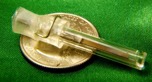
The following image is  the researchers’ new sensor, balanced on a coin,

Researchers have created a new type of miniature pressure sensor, shown here, designed to be implanted in the body. Acoustic waves from music or plain tones drive a vibrating device called a cantilever, generating a charge to power the sensor. (Birck Nanotechnology Center, Purdue University)

I found the description of how the cantilever works and can be recharged quite interesting,

The heart of the sensor is a vibrating cantilever, a thin beam attached at one end like a miniature diving board. Music within a certain range of frequencies, from 200-500 hertz, causes the cantilever to vibrate, generating electricity and storing a charge in a capacitor …

The cantilever beam is made from a ceramic material called lead zirconate titanate, or PZT, which is piezoelectric, meaning it generates electricity when compressed. The sensor is about 2 centimeters long …

A receiver that picks up the data from the sensor could be placed several inches from the patient. Playing tones within a certain frequency range also can be used instead of music.

“But a plain tone is a very annoying sound,” Ziaie said. “We thought it would be novel and also more aesthetically pleasing to use music.”

Researchers experimented with four types of music: rap, blues, jazz and rock.

“Rap is the best because it contains a lot of low frequency sound, notably the bass,” Ziaie said.

“The music reaches the correct frequency only at certain times, for example, when there is a strong bass component,” he said. “The acoustic energy from the music can pass through body tissue, causing the cantilever to vibrate.”

When the frequency falls outside of the proper range, the cantilever stops vibrating, automatically sending the electrical charge to the sensor, which takes a pressure reading and transmits data as radio signals. Because the frequency is continually changing according to the rhythm of a musical composition, the sensor can be induced to repeatedly alternate intervals of storing charge and transmitting data.

“You would only need to do this for a couple of minutes every hour or so to monitor either blood pressure or pressure of urine in the bladder,” Ziaie said. “It doesn’t take long to do the measurement.”

It’s usually a long time from testing a concept (in this case, on a water balloon) to bringing a product to the marketplace. In the meantime, I wonder if this concept will work in the ‘wild’ where people are exposed to rap music accidentally or they like to listen to it themselves, all day long, or they loathe rap music and don’t want to listen for a few minutes every hour.

Finally, I have some special appreciation for Venere as he very neatly explained terms I’ve seen many times but for which I’ve only been able to find complicated definitions. Thank you, Mr. Venere and for a very clear description of this technology.

Fundamentals of nanoelectronics at nanoHUB-U

nanoHUB is a project hosted by Purdue University’s (Indiana, US) Network for Computational Nanotechnology. A successful online community has been created over a number of years. My Nov. 16, 2010 posting noted that they had over 150,000 users at that time. Their latest (Dec. 2, 2011) newsletter notes a new initiative, nanoHUB-U,

We are launching a series of online short courses on nanoscience and nanotechnology that will be offered over the next couple of years. This initiative builds on the open content we have on nanoHUB.org. We think the approach is unique – the courses are designed to be broadly accessible without many prerequisites, and the material is presented in an original way. Students get access to a completely new set of lectures not available on nanoHUB, extensive lecture notes, exams, homeworks, Q & A forums, and exercises using nanoHUB tools.

We’re starting with Prof. Supriyo Datta’s Fundamentals of Nanoelectronics on January 23, 2012.

Here’s a little more information about the course from the registration page,

Fundamentals of Nanoelectronics Part I: Basic will be the first offering of two, five-week online courses. This offering is based on unique courses developed at Purdue, whose videotaped lectures posted on the nanoHUB have attracted 75,000+ viewers since 2004, with enthusiastic reviews. Part I is accessible to anyone familiar with calculus and elementary differential equations.

Here’s a little information about the instructor,

Supriyo Datta is the Thomas Duncan Distinguished Professor at the School of Electrical and Computer Engineering, Purdue University. He is a Fellow of the IEEE (Institute for Electrical and Electronics Engineers) and the APS (American Physical Society) and his books

  1. Electronic Transport in Mesoscopic Systems, Cambridge (1995)
  2. Quantum Transport: Atom to Transistor, Cambridge (2005)

are standard in the field. This course is based on his soon to be published book

* Lessons from Nanoelectronics: A New Perspective on Transport, World Scientific (2012)

which seeks to convey the key concepts to non-specialists.

He has received IEEE Technical Field Awards both for research and for graduate teaching and was recently awarded the Procter Prize for “outstanding contribution to scientific research and demonstrated ability to communicate the significance of this research to scientists in other disciplines.”

This course is $30US.

Atomic force microscopy and uncertainty

Michael Berger at Nanowerk writes about the importance of determining uncertainty in his Nov. 11, 2011 article, A framework to evaluate the uncertainties of AFM nanomechanical measurements, on Nanowerk. It may seem oxymoronic trying to evaluate uncertainty but it’s done all the time.Take for example a political poll where they tell you how accurate it is likely to be, “19 times of 20.”  For another example, there’s also significance (p value) when analyzing statistical data. Here’s a brief description of p value from GraphPad,

Definition of a P value

Consider an experiment where you’ve measured values in two samples, and the means are different. How sure are you that the population means are different as well? There are two possibilities:

  • The populations have different means.
  • The populations have the same mean, and the difference you observed is a coincidence of random sampling.

The P value is a probability, with a value ranging from zero to one. It is the answer to this question: If the populations really have the same mean overall, what is the probability that random sampling would lead to a difference between sample means as large (or larger) than you observed?

Many people misunderstand what question a P value answers.

If the P value is 0.03, that means that there is a 3% chance of observing a difference as large as you observed even if the two population means are identical. It is tempting to conclude, therefore, that there is a 97% chance that the difference you observed reflects a real difference between populations and a 3% chance that the difference is due to chance. Wrong. What you can say is that random sampling from identical populations would lead to a difference smaller than you observed in 97% of experiments and larger than you observed in 3% of experiments.

You have to choose. Would you rather believe in a 3% coincidence? Or that the population means are really different?

In other words, which one has greater certainty? Getting back to nanotechnology, there’s this from Berger’s article,

“The atomic force microscope is used extensively for measuring the material properties of nanomaterials with nanometer resolution, unfortunately there is a lack of standards and uncertainty quantification in these measurements,” explain Robert Moon, an Adjunct Assistant Professor of Materials Engineering, and Arvind Raman, Professor of Mechanical Engineering, both at Purdue University. “Other fields, such as six sigma standards in industry and beam corrections in scanning electron microscopy, have developed thorough methods for quantifying the uncertainty in a given measurement, model, or system. Broadly speaking these methods can be classified as uncertainty quantification. Without applying the methods of uncertainty quantification to AFM measurements it is impossible to say if the measurements are accurate within 5% or 100%.”

Moon and Raman at Purdue’s Birck Nanotechnology Center and collaborators at the National Institute of Standards and Technology (NIST) including Drs. Jon Pratt and Gordon Shaw, have now presented a framework to ascribe uncertainty to local nanomechanical properties of any nanoparticle or surface measured with the AFM by taking into account the main uncertainty sources inherent in such measurements.

“Our findings demonstrate the inherently large uncertainty associated with certain types of AFM material property measurements,” Ryan Wagner, a graduate student in Raman’s group at Purdue, and the paper’s first author, tells Nanowerk. “Specifically, force-displacements measurements of elastic modulus on thin, stiff samples are very uncertainty because of poor indentation resolution. In addition, our work provides a general framework for evaluating uncertainty in force-displacement based elasticity measurements that is valid for all samples and AFMs.”

Berger’s article offers more details about the process of arriving at a framework for uncertainty and a link to the researchers’ paper.

nanoHUB; growing an online community?

I joined the nanoHUB ages ago (Sept. 2007) and haven’t paid much attention until recently when they sent me a survey to analyze my needs and, a few weeks after that, sent me a newsletter. Still, I was a bit surprised to find out they have 150,000 users on their hub and are now canvassing for people to join a user group (from the Nov. 12 2010 news item on Nanowerk),

To better serve its more than 150,000 users this year, nanoHUB.org is establishing a User Group to serve as a forum to facilitate the exchange of ideas among nanoHUB users.

The inaugural User Group meeting will be Wednesday, December 8, 2010, at the Westin Arlington Gateway hotel in Arlington, Virginia. The meeting will begin at 3:30 p.m., and will be in conjunction with the National Science Foundation’s Nanoscale Science and Engineering Grantees Conference. Registration is required to attend and may be made at https://nanohub.org/eventregistration/.

The meeting topics will be: “150,000 Users and Growing: A nanoHUB.org Overview”; “nanoHUB.org: Real Users and Real Stories”; and “The Future of nanoHUB.org”. nanoHUB.org users are invited to attend.

Members of the User Group include representatives from education, research and industry. Insight gathered from the user Group will help guide selection of content, improve the understanding of user needs, and accelerate the evolution of nanoHUB.

nanoHUB.org is funded by the National Science Foundation, is a project of the Network for Computational Nanotechnology which, according to its contact page, is located at the University of Purdue in Indiana (US).

There is an August 2007 ELI paper (No. 7) written by Carie Windham for EDUCAUSE which gives a history and some insight into nanoHUB’s development,

In 2002, when Purdue University researchers merged the six-year-old Purdue University Network Computing Hubs (PUNCH) with the mission of the NSF’s Network for Computational Nanotechnology (NCN), scientists saw, from the beginning, a new frontier for computational science. What would happen, they wondered, if researchers in the field of nanotechnology (the study of particles 25,000 times smaller than the width of a human hair) could harness the power of grid computing to provide a single entry point to scientific tools, discoveries, and research on the Web without forcing the user to download a single piece of code?

The fruits of that marriage became the nanoHUB (http://www.nanohub.org/), a Science Gateway1 for researchers, faculty, and students in nanotechnology. Taking advantage of PUNCH’s extensive cyberinfrastructure and later that of TeraGrid—which employs supercomputers and data storage at nine partner sites—the nanoHUB portal enables users to access scientific tools for research, demonstration, and collaboration. It also serves as a resource for nanotechnology workshops, lectures, and curricula. Users can run experiments, brush up on nanotechnology research, or download a series of undergraduate lectures meant to explain the science at a level appropriate for novices.

The nanoHUB site has to lots to offer even if you’re not a member or particularly scientific and it could even provide an interesting case study for developing online communities.