Category Archives: marketing

Self-cleaning schools

I’m all for self-cleaning, which is why this Apr. 19, 2013 news item on Azonano caught my attention,

“We’re always trying to create a cleaner environment for students and teachers in an effort to reduce absenteeism and the associated costs,” says Dr. Henry Kiernan, Superintendent with the Bellmore-Merrick School District in New York. “The NanoTouch® products provide an additional benefit of communicating our commitment, which plays an important role in our relationship with parents.”

Bellmore-Merrick has installed facility touch points, including door push pads and handle wraps, on all bathroom doors in an initial 5 high schools. Other schools have brought the portable NanoSeptic surfaces into the classroom in the form of snack mats and desk mats.

“The pre-school students were fascinated by the snack mats and what they did. The children focused intently on keeping their snacks on the mat,” says Bonny Phillips , teacher at Liberty Christian Academy’s Early Learning Center. “It also provided an additional opportunity for learning about cleanliness and food handling.”

“Schools will continue to use one-time kill products like disinfectants, but NanoTouch enhances their cleaning efforts by working to eliminate even hard-to-kill microbes such as C. Diff, 24 hours a day, seven days a week,” says Mark Sisson , co-founder of NanoTouch. “And because alcohol based hand sanitizers pose a risk of fire around kids, NanoTouch products help to fill that void in schools.”

In today’s world of shrinking budgets, it’s sometimes difficult for schools to find funding for advanced technologies like NanoTouch, even when these products are inexpensive. However, some innovative thinking by a community bank has led to several classrooms being equipped with NanoSeptic snack mats. SelectBank, headquartered in Forest, Virginia, donates snack mats to area pre-schools and day cares as a way to give back to their community.

“When we can help area schools and children, and get some positive recognition from parents, that’s good for our community and for our business,” says Sherri Sackett , Marketing Manager at SelectBank.

And the parents at these schools are enthusiastically embracing the use of this new nanotechnology.

“We were very excited to hear that our son’s school has started using this new product,” says Robert Thomas, parent of a student at the Blue Ridge Montessori School. “Not only is this creating a cleaner classroom environment for our child, but it’s doing so in a healthier way, without poisons or heavy metals. And it’s such a unique product line that the school is considering selling the travel kits as a fundraiser.”

“NanoTouch is out to make the world a better and healthier place to live, work, and play. This is particularly important for sensitive populations, such as our youth,” says NanoTouch co-founder, Dennis Hackemeyer. “And, what can’t be understated is the communications ability of NanoTouch products to educate and change behavior.'”

It’s unusual these days to see a company market a ‘nanotechnology’ product by incorporating nano into  product names (e.g., NanoSeptic) and the company name (NanoTouch).

The NanoTouch website does not offer information about its management team (I was not able to find either co-founder although it is possible to find a listing for the company’s advisory board) nor is there much information about the technology. Here’s the best technology description I could find on the website, from the NanoTouch NanoSeptic versus other antimicrobials page,

NanoTouch products utilize several complex components which all work together. Our specialized fabrication process not only provides products that are durable enough to withstand routine cleaning, but also helps to accentuate the effectiveness of the antimicrobial ingredients and maximize the surface’s self-cleaning action. Our products contain widely used, harmless, “green” chemistry, which does not include diluted poisons or heavy metals. The antimicrobial technology we deploy, molecularly bonded on a nano-scale, provides a non-leaching, self-cleaning surface that constantly traps and kills bacteria, viruses and fungi through a catalytic oxidation process using available light.

All of these solutions approach the problem of bacteria, viruses and fungus by cleaning surfaces…which is absolutely necessary. NanoTouch is not meant to replace these methods, but instead, it is a perfect complement and another step in the reduction of germ transfer. While the these approaches clean a touchpoint or a person’s hand, contamination happens with the next contact or from airborne microbes. NanoTouch self-cleans…constantly killing bacteria, viruses and fungi.

I did find some details about the company co-founders on their respective  LinkedIn pages, Dennis Hackemeyer and Mark Sisson. Both men are associated with another company, KiteString, from the Our Approach page,

KiteString uses innovative technological solutions in the service of creative to achieve Marketing Relevance. Yes, we deliver traditional creative services like design, Web development, and direct mail, but we also provide technology-based marketing solutions and client service processes and systems that deliver measurably better operational efficiency, enhanced brand management, improved collaboration and greater marketing response rates.

I’m not sure what the KiteString description of their approach means but it looks like KiteString’s main activity is marketing. Anyway, that’s not so important given that my main interest is NanoTouch. For that matter, it would have been nice to have found more technical information. For example, How precisely is this product nanotechnology-enabled? Are there scientists working for or associated in some fashion with NanoTouch? What kind of testing has the product undergone? These are a few of the questions that leap to mind.

WAVE in Alberta (Canada); bringing your technology products to market

May 5 – 8, 2013 are the dates for WAVE 2013, Alberta’s technology commercialization conference, being held at the Fairmont Chateau in Lake Louise, Alberta. The conference features 12 keynote speakers from industry (including Dr. Wagiuh Ishak of Corning Inc, Dr. Sergio Kapusta of Royal Dutch Shell, Stephen Graham of Maple Leaf Foods, and Travis Earles of Lockheed Martin) discussing 6 market areas (including health/medical, cleantech/conventional energy and agriculture/forestry).

The conference host and organizer is ACAMP (Alberta Centre for Advanced Micro and Nano Technology Products) a not-for-profit centre offering business support to micro and nano technology businesses. WAVE 2013 is the second such conference, the first being held in 2011. From the About WAVE page on the conference website,

From a Ripple in Research to a Powerful Wave in Marketing

The WAVE 2013 Conference and Exhibition builds on the success of our last conference WAVE 2011. WAVE 2013 exists to enable and encourage companies with investable hardware product technologies to showcase their state-of-the-art capabilities and bring them to market. There will be no poster sessions, academic papers, or student presentations.

Professionals representing domestic and international corporations are invited to take exhibitor space in order to network with other market strategists, distributors and representatives, manufacturers, materials producers, equipment suppliers, and investors.

This is an opportunity to expand your market and showcase your products. Networking areas are available free of charge and designed to allow attendees to meet privately to discuss business opportunities.

The bottom-line goal is bottom-line success.

The WAVE home page description offers more specifics as to how this conference is organized to maximize contact between participants,

Take your investable tech products to market

You may have a great investable technology product and not know it yet. Or you may know it, but can’t find partners and markets. In either case, it’s a big challenge to connect innovators with larger corporations and funding to help develop products and take them to market.

That’s what the Wave 2013 conference is all about… and we’re doing it in a very different way.
Connect with the right exhibitors

Typically, at large international conferences the exhibitors exhibit. The presenters present. The attendees listen and walk around exhibits looking for opportunities. Everyone is left to their own devices to make the right connections.

But at Wave 2013, we’re going to change all that. Every company that exhibits will also present to the entire audience. So exhibitors and attendees will understand where the opportunities are without all the frustration.
Actually meet the keynotes one-on-one

What about the big keynotes? There will be outstanding keynotes from a who’s who in the international tech space. And get this… they won’t just present and go home. At the presentations you’ll learn what they’re looking for and then they’ll be available for one-on-one meetings with you during the three days.

Plus, government officials from Alberta and across Canada will be in attendance, looking for new opportunities to invest and collaborate.
Find the right partners

So come. Exhibit. Present. Or join us as an attendee and pitch your product in one-on-one meetings. Some of the world’s most important companies in the tech space want to tell you what they’re looking for and hear about what you’re working on.

You can find more information about the conference in a brochure which oddly enough is on the NanoQuébec website here (scroll down about 1/3 of the way). I couldn’t find the brochure or the list of industry keynote speakers on the WAVE 2013 conference website (?)

Carbon nanotubes, helicopters, and Ethan Chu (winner of the second annual Sikorsky Helicopter 2050 Challenge)

The Dec. 15, 2012 news item on Azonano about the winner of the 2nd annual Sikorsky 2050 Helicopter Challenge provides details about the contest, its theme, and the winning entry (which includes carbon nanotubes as part of its solution to creating an environmentally friendly helicopter),

The Igor Sikorsky Youth Innovator Award is the grand prize for the Sikorsky Helicopter 2050 Challenge, a national competition started in 2011 sponsored by Sikorsky Aircraft and By Kids For Kids. This year’s program challenged youths ages 9-16 across the U.S. to envision an environmentally friendly helicopter. The competition rated designs for concept uniqueness, description detail and creativity of the presentation.

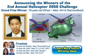
Ethan portrays his winning design as a compact, circular-shaped twin-engine helicopter dubbed the AH-9 Diamondback. High strength materials in the form of lightweight carbon nanotubes covered with titanium panels comprise the helicopter’s structure, a design approach that reduces the aircraft’s weight and fuel consumption, and improves its carrying capacity. His environmentally friendly design further reduces carbon footprint by channeling engine exhaust along the rotor blades and around the body of the aircraft to provide a cushion of gas for additional lift — an aerodynamic principle known as the Coanda Effect.

“We were impressed with the strong scientific reasoning and the good deal of thought that Ethan put into his innovative submission,” said Vern Van Fleet , a chief test engineer for Sikorsky Military Systems. “And he never lost sight of the competition theme, which was to produce an environmentally friendly helicopter.”

From the 2nd Annual Helicopter 2050 Challenge home page

Winners of the 2nd (2012) Annual Helicopter 2050 Challenge

Winners of the 2nd (2012) Annual Helicopter 2050 Challenge

Here’s more about the winning design from the contest winners page on the Challenge website,

Ethan C., Age: 16; Idea: AH-9 Diamondback

The AH-9 Diamondback is a round shaped helicopter that utilizes the “Coanda” effect phenomena. A fan pushes the air down and out at high speed around the body creating a low pressure area around the top of the helicopter, which then creates an extra lift. Two turbofans power the aircraft and two stub wings under the cockpit enhance control and stability at high speed. A four-bladed rotor on top provides the main lift. The blades have symmetrical airfoil cross-sections, allowing for less drag. The aircraft uses carbon nanotubes resulting in a very light design, which reflects high fuel efficiency and improved load-carrying capacity. The design also includes a “med-vac” for evacuating wounded troops which includes space for a medic and two patients.

Chu won a $1000 scholarship prize and an all-expenses paid trip for two (he went with his father) to Sikorsky’s headquarters in Stratford, Connecticut.

Here’s a description of the company sponsoring the challenge from the About Sikorsky webpage,

Sikorsky Aircraft Corporation is a world leader in the design, manufacture and service of military and commercial helicopters; fixed-wing aircraft; spare parts and maintenance, repair and overhaul services for helicopters and fixed-wing aircraft; and civil helicopter operations.

A passion for aviation drove immigrant Igor Sikorsky to establish The Sikorsky Manufacturing Corporation in 1925 on Long Island, New York, and the company later became The Sikorsky Aviation Corporation. In 1929, Igor purchased land in Stratford, Connecticut, and the company became a subsidiary and later a division of United Aircraft Corporation, which evolved into United Technologies Corporation in 1975.

Today, Sikorsky Aircraft Corp. stays true to the legacy of Igor Sikorsky with a mission statement that encompasses his passion for safety and innovation: “We pioneer flight solutions that bring people home everywhere…every timeTM.” Sikorsky helicopters have saved an estimated 2 million lives since performing the world’s first helicopter rescue in 1944.

Sikorsky helicopters are used by all five branches of the United States armed forces, along with military services and commercial operators in 40 nations. Core U.S. military production programs are based on the Sikorsky H-60 aircraft: the BLACK HAWK helicopter for the U.S. Army and SEAHAWK® helicopter for the U.S. Navy. H-60 aircraft derivative aircraft perform multiple missions with other branches of the U.S. military. The CH-53E helicopter and MH-53E helicopter heavy-lift aircraft are flown by the U.S. Navy and Marine Corps to transport personnel and equipment, and in anti-mine warfare missions. Sikorsky is currently developing the next-generation CH-53K helicopter for the U.S. Marines.

Sikorsky has developed four generations of maritime helicopters including the proven SEAHAWK, SUPER STALLION™ and SEA KING™ helicopters that support the maritime operations of navies across the globe. Sikorsky has designed and built nearly half of all such helicopters currently serving with armed forces throughout the world.

BLACK HAWK helicopter variants are serving with 25 governments worldwide: Argentina, Australia, Austria, Bahrain, Brazil, Brunei, Chile, Colombia, Egypt, Greece, Israel, Japan, Jordan, Malaysia, Mexico, Morocco, People’s Republic of China, the Philippines, Republic of Korea, Saudi Arabia, Spain, Taiwan, Thailand, Turkey and the U.S.

By Kids For Kids Co., also mentioned in the news item as one of the sponsors for the 2050 Helicopter Challenge, is an ‘Educational and Family Marketing Company’ and “[it] provides innovative and integrated in-school marketing programs to help clients meet corporate social responsibility goals” according to the descriptor provided by the Yahoo search engine (http://search.yahoo.com/search?p=by+kids+for+kids&ei=UTF-8&fr=moz35).

Bot bot here and bot bot there and a bot bot everywhere but not Old Macdonald’s Farm

The Materials Research Society (MRS) has a Fall 2011 meeting in Boston, Massachusetts scheduled for Nov. 28, 2011 to Dec. 2, 2011, which will feature amongst other exhibits,  ‘mibots’. From the Nov. 9, 2011 news item on Azonano,

…  new “miBots” from Imina Technologies (Ecublens, Switzerland).

.. are more than nanomanipulators. Unlike conventional systems, they are virtually untethered and move independently. Working individually or in groups, they can be fitted with a variety of tools such as grippers, probes, and optical fibers so that, in addition to manipulating the sample, they can illuminate a nano workspace and conduct force or electrical measurements. Vacuum ready, miBots’ proprietary monolithic structure makes them robust, mechanically and thermally stable, and less sensitive to vibration.

Imina Technologies has engineered a variety of stage options for these novel mini robots. For conventional installation on inverted light microscopes (LM), SEMs, or focused-ion beam systems (FIBs), the “miBase” provides control and maneuvering room for up to four miBots. Special apertures accommodate illumination for the LM and stubs for SEMs, and multiple coaxial I/O connections enable electrical characterization and testing.

You can find out more about Imina Technologies and their ‘mibots’ here.

For a completely different kind of bot, a company named Nanobotmodels, situated in the Ukraine, offers illustration, animations, and presentation materials. From the company’s About page,

Our company Nanobotmodels was founded in 2007 and its goal is todevelop modern art-science-technology intersections. Nanotechnology boosts medicine, engineering, biotechnology, electronics soon, so artwork and vision of the nanofuture will be very useful.

We are making hi-end nanotechnology and nanomedicine illustration and animation. You can imagine any interesting-to-you animation, illustration or presentation materials, and we can make them real.

The level of detail in each medical illustration can be used to simplify complex structures and make them visually attractive.

Our clients include the largest medicine photobanks, nanotechnology magazines and publications, educational organization, and private companies.

Company was founded by CEO Svidinenko Yuriy, futurist and nanotechnology artist.

Our team consists of modern artists, modelers and nanotechnology scientists.

Here’s a bit more about the company’s work in medical illustration from a Nov. 11, 2011 news item at Nanotechnology Now,

One heat therapy to destroy cancer tumors using nanoparticles is called AuroShell™. The AuroShell™ nanoparticles circulate through a patient’s bloodstream, exiting where the blood vessels are leaking at the site of cancer tumors. Once the nanoparticles accumulate at the tumor the AuroShell™ nanoparticles are used to concentrate the heat from infrared light to destroy cancer cells with minimal damage to surrounding healthy cells. Nanobotmodels company provides good visual illustration of this process. Nanospectra Biosciences has developed such a treatment using AuroShell™ that has been approved for a pilot trial with human patients.

Gold nanoparticles can absorb different frequencies of light, depending on their shape. Rod-shaped particles absorb light at near-infrared frequency; this light heats the rods but passes harmlessly through human tissue. Sphere-shaped nanoparticles absorb laser radiation and passes harmlessly through human tissue too.

Nanobotmodels Company provides visual illustration of nanoparticle cancer treatment. Our goal – make realistic vision of modern drug delivery technology.

I found this sample on the company’s website gallery,

Illustration from Nanobotmodels website: Nanomechanical robots attacking cancer cell

You can find more artwork here.

Those are all the bots for today.

Intel, 32nm chips, slick marketing, and ‘ripplecasting’

I first came across the marketing campaign for Intel®’s 2nd generation Core™ Processor Family via a fun fact sheet. From the Feb. 25, 2011 news item on Nanowerk,

Last year, Intel unveiled its Core™ processor family that, for the first time, used a full-featured system-on-a-chip 32 nanometer process technology to complement the CPU-specific technology. …

# A nanometer is so small that it takes a billion of them to make a meter. A billion is a huge number. A stack of a billion sheets of paper would be 100 km high. If you could walk a billion steps, you would go around the earth 20 times.

# The original transistor built by Bell Labs in 1947 was large enough that it was pieced together by hand. By contrast, more than 60 million 32nm transistors could fit onto the head of a pin. (A pin head is about 1.5 mm in diameter)

# More than 4 million 32nm transistors could fit in the period at the end of this sentence. (A period is estimated to be 1/10 square millimeter in area)

# Compared to Intel’s first microprocessor, the 4004, introduced in 1971, a 32nm CPU runs over 4000 times as fast and each transistor uses about 4000 times less energy. The price per transistor has dropped by a factor of about 100,000.

The marketing piece that has really excited my interest is The Chase Film,

What I find particularly interesting about this marketing campaign is the number of channels, the variety of materials, the time frame, and the range of audiences being addressed. Apparently the film (which is a remarkably slick production that crosses platforms seamlessly from live action to animation to a game format to Google Earth to Facebook and so on in the context of a ‘chase’ story) was presented yesterday at TED 2011 the same day it started, March 1, 2011 while at least one version of the film was posted on Youtube 2 months ago.

There’s more promotional material here at Intel Unveils All New 2010 Intel® Core™ Processor Family including quotes, images and, at least one more, video.

It looks to me like they are simultaneously ‘narrowcasting’ and ‘broadcasting’ to their audiences and this is an approach I heartily agree with. I know it’s fashionable in ‘communications’ circles to say that there is no such thing as a general audience which is why communication should be targeted to specific audiences. Two big issues arise with this kind of thinking (a) a tendency to preach to the converted and (b) a failure to properly identify the audiences.

Taking Intel as my example, that company broke ground when it started advertising its computer chips on television.  While dumbfounding the rest of the industry, Intel took the computer chip into daily conversation. I don’t know how they bought the media but I am assuming there was some strategy regarding the programmes they chose for their early advertising breaks. In essence, the advertising was both general and targeted and identified an audience that no one else in the industry though existed.

You could say this new marketing strategy is general and targeted. Placing the video on Youtube is sending it out to the ‘general’ public. The concept behind the video is very engaging and as I noted, this is a very slick cross-platform piece. It’s the type of work you want to look at several times so you can catch everything.

Bringing the video (I gather one of the speakers is from Intel ETA Mar.4.11, I was wrong; it’s one of 10 winners of their “Ads worth spreading competition“) to TED (Technology Education Design) 2011 could be considered narrowcasting since only registrants (able to pay a high registration fee, interested in cutting edge ideas, and innovative thinkers) will see it at this time (these talks are made available for free months later). The registrants  and the speakers for an event of this nature could be viewed as ‘influencers’. In other words, people who are ‘cool’ and whom others will follow. As you do, for example,  on Twitter which is how I found this video.

I think I’m going to coin a phrase, ‘ripplecasting’ to describe what Intel is doing here. You throw a stone in the water and it causes ripples just like sending a speaker to TED 2011 where a registrant tweets (comments on their Twitter feed) which gets retweeted and so on. Sending a ‘fun’ factsheet to Nanowerk, is targeted communication to the nanotechnology community gets us back to narrowcasting.

ETA Mar.3.11: In rereading the previous passage, I think I wasn’t as clear about my ‘ripplecasting’ concept as I’d thought but then I am in the process of developing it.  Here I go again, ripplecasting is a way of describing narrowcasting, broadcasting, and the use of new media and social media. I think Intel’s new product provides an excellent example of ‘ripplecasting’ with its use of tv advertising, outreach to industry media, presentation at TED 2011 which gets tweeted, and so on it goes.

I mentioned time frames earlier, this the 2nd year of Intel’s campaign, they unveiled their new product family in Jan. 2010.

Bravo Intel!

Marketing, safety, and nanotechnology plus there’s another Synthetic Bio event

There’s a new study that suggests that scientists and the general public (in the US) have differing attitudes to nanotechnology. The study conducted by Dietram Scheufele and Elizathe Corley (professors from the University of Wisconsin-Madison and Arizona State University, respectively) shows that scientists are focusing on potential risks and economic values while the public is focusing on potential benefits when asked about regulating nanotechnology. More details about the study and where it’s been published can be found here on Azonano.

This information provides an interesting contrast to a media release about a conference in Brussels (June 10, 2009) where Dr. Andrew Maynard, Chief Science Advisor for the Project on Emerging Nanotechnolgies, expressed concern that companies in Europe are beginning to drop the mention of nanotechnologies on product labels.

“We have seen some companies drop the ‘nano’ claim while continuing to use nanotechnology. This suggests nanotechnology is going underground,” [Maynard]said.

Harald Throne, researcher at the National Institute for Consumer Research in Norway, echoed concerns that companies may be becoming less inclined to highlight nanomaterials.

He searched a website run by a major international cosmetics company, using keywords like ‘nanotechnology’ and ‘nano’, to estimate how many products contain nanotechnology. Throne’s search turned up 29 products in 2007, but when he repeated the same exercise recently, there were zero hits.

This, he said, suggests that companies may now view ‘nano’ as a negative label rather than an added value.

You can read more about it here on the Euractiv website. I couldn’t find the Brussels conference they mention but maybe you’ll have better luck.

These contrasting reports would suggest that attitudes in Europe differ from attitudes in the US where we’re discussing the general public. I make this inference from the fact that companies in Europe are not making the nanotechnology claim and presumably that is because they are concerned about the public’s attitude.  It should be noted that a European industry representative quoted in the media release claims that the problem lies with the difficulty of actually defining a nanomaterial. The representative does have  a point of sorts. Still, I do wonder why companies were able to make the nanotechnology claim in 2007 despite the lack of definitions.

There’s a synthetic biology event coming up this Wednesday, June 24, 2009, 9:30 am. to 10:30 am PST.

When
Wednesday, June 24, 2009, 12:30-1:30 PM (light lunch available at 12 noon)
Who
Erik Parens, Senior Research Scholar, The Hastings Center
Gregory Kaebnick, Research Scholar, The Hastings Center
David Rejeski, Moderator, Director, Synthetic Biology Project
The emerging field of synthetic biology will allow researchers to create biological systems that do not occur naturally as well as to re-engineer existing biological systems to perform novel and beneficial tasks. Synthetic biology promises significant advances in areas such as biofuels, specialty chemicals, agriculture, and medicine but also poses potential risks. As the science and its applications develop, a comprehensive approach to addressing ethical and social issues of emerging technologies as a whole is called for if scarce intellectual resources are to be used optimally, according to a new report authored by Erik Parens, Josephine Johnston, and Jacob Moses of The Hastings Center.
In Ethical Issues in Synthetic Biology: An Overview of the Debates, the authors examine how the ethical issues raised by a variety of emerging technologies are often similar and familiar.  They find that these similarities are abundant enough to justify an effort to develop an ethical framework that cuts across emerging and converging technologies.  Indeed, rather than stovepiping ethical questions into the hyphenated areas of bio-ethics, nano-ethics, neuro-ethics and so on, it is time to begin speaking about the ethics of emerging technologies as a whole.
On June 24, Erik Parens will discuss the report’s findings, exploring the differences between physical and non-physical harms and pro-actionary and pre-cautionary frameworks, in an effort to better define the ethical issues around synthetic biology.  Gregory Kaebnick, also of The Hastings Center, will describe the Center’s new, multi-year project that will examine the ethical issues raised in the report in greater depth.