Tag Archives: Boris I. Yakobson

To make carbon nanotubes (CNTs), reach like a giraffe

Caption: There are dozens of varieties of nanotubes, each with a characteristic diameter and structural twist, or chiral angle. Carbon nanotubes are grown on catalytic particles using batch production methods that produce the entire gamut of chiral varieties, but Rice University scientists have come up with a new strategy for making batches with a single, desired chirality. Their theory shows chiral varieties can be selected for production when catalytic particles are drawn away at specific speeds by localized feedstock supply. The illustration depicts this and an analogous process 19th-century scientists used to describe the evolution of giraffes’ long necks due to the gradual selection of abilities to reach progressively higher for food. Credit: Illustration by Ksenia Bets/Rice University

A November 9, 2022 Rice University news release (also on EurekAlert) announces the Holy Grail (I’ve lost track of how many have been reached) has been achieved for growing batches of carbon nanotubes,

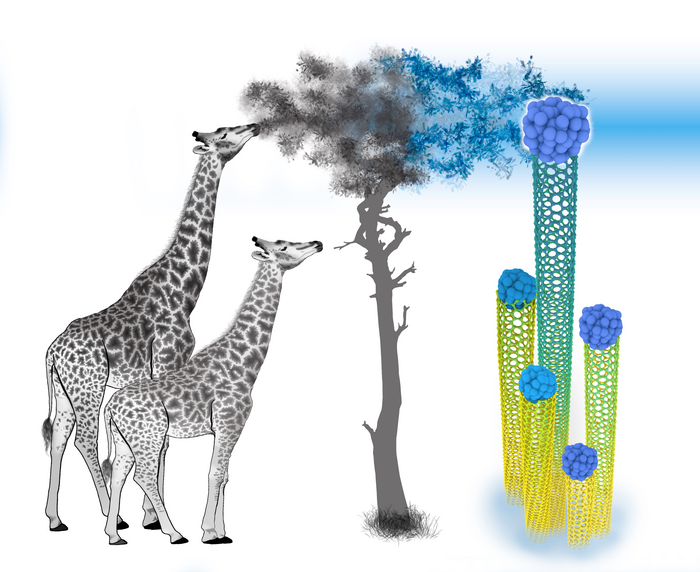
Like a giraffe stretching for leaves on a tall tree, making carbon nanotubes reach for food as they grow may lead to a long-sought breakthrough.

Materials theorists Boris Yakobson and Ksenia Bets at Rice University’s George R. Brown School of Engineering show how putting constraints on growing nanotubes could facilitate a “holy grail” of growing batches with a single desired chirality.

Their paper in Science Advances describes a strategy by which constraining the carbon feedstock in a furnace would help control the “kite” growth of nanotubes. In this method, the nanotube begins to form at the metal catalyst on a substrate, but lifts the catalyst as it grows, resembling a kite on a string.

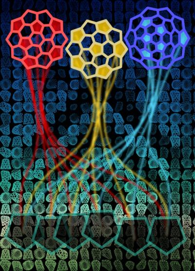
Carbon nanotube walls are basically graphene, its hexagonal lattice of atoms rolled into a tube. Chirality refers to how the hexagons are angled within the lattice, between 0 and 30 degrees. That determines whether the nanotubes are metallic or semiconductors. The ability to grow long nanotubes in a single chirality could, for instance, enable the manufacture of highly conductive nanotube fibers or semiconductor channels of transistors.

Normally, nanotubes grow in random fashion with single and multiple walls and various chiralities. That’s fine for some applications, but many need “purified” batches that require centrifugation or other costly strategies to separate the nanotubes.

The researchers suggested hot carbon feedstock gas fed through moving nozzles could effectively lead nanotubes to grow for as long as the catalyst remains active. Because tubes with different chiralities grow at different speeds, they could then be separated by length, and slower-growing types could be completely eliminated.

One additional step that involves etching away some of the nanotubes could then allow specific chiralities to be harvested, they determined.

The lab’s work to define the mechanisms of nanotube growth led them to think about whether the speed of growth as a function of individual tubes’ chirality could be useful. The angle of “kinks” in the growing nanotubes’ edges determines how energetically amenable they are to adding new carbon atoms.

“The catalyst particles are moving as the nanotubes grow, and that’s principally important,” said lead author Bets, a researcher in Yakobson’s group. “If your feedstock keeps moving away, you get a moving window where you’re feeding some tubes and not the others.”

The paper’s reference to Lamarck giraffes — a 19th-century theory of how they evolved such long necks — isn’t entirely out of left field, Bets said.  

“It works as a metaphor because you move your ‘leaves’ away and the tubes that can reach it continue growing fast, and those that cannot just die out,” she said. “Eventually, all the nanotubes that are just a tiny bit slow will ‘die.’”

Speed is only part of the strategy. In fact, they suggest nanotubes that are a little slower should be the target to assure a harvest of single chiralities.

Because nanotubes of different chiralities grow at their own rates, a batch would likely exhibit tiers. Chemically etching the longest nanotubes would degrade them, preserving the next level of tubes. Restoring the feedstock could then allow the second-tier nanotubes to continue growing until they are ready to be culled, Bets said.

“There are three or four laboratory studies that show nanotube growth can be reversed, and we also know it can be restarted after etching,” she said. “So all the parts of our idea already exist, even if some of them are tricky. Close to equilibrium, you will have the same proportionality between growth and etching speeds for the same tubes. If it’s all nice and clean, then you can absolutely, precisely pick the tubes you target.”

The Yakobson lab won’t make them, as it focuses on theory, not experimentation. But other labs have turned past Rice theories into products like boron buckyballs.

“I’m pretty sure every single one of our reviewers were experimentalists, and they didn’t see any contradictions to it working,” Bets said. “Their only complaint, of course, was that they would like experimental results right now, but that’s not what we do.”

She hopes more than a few labs will pick up the challenge. “In terms of science, it’s usually more beneficial to give ideas to the crowd,” Bets said. “That way, those who have interest can do it in 100 different variations and see which one works. One guy trying it might take 100 years.”

Yakobson added, “We don’t want to be that ‘guy.’ We don’t have that much time.”

Here’s a link to and a citation for the paper,

Single-chirality nanotube synthesis by guided evolutionary selection by Boris I. Yakobson and Ksenia V. Bets. Science Advances 9 Nov 2022 Vol 8, Issue 45 DOI: 10.1126/sciadv.add4627

This paper is open access.

A gas, gas, gas for creating semiconducting nanomaterials?

A June 14, 2021 news item on phys.org highlights some new research from Rice University (Texas, US),

Scientific studies describing the most basic processes often have the greatest impact in the long run. A new work by Rice University engineers could be one such, and it’s a gas, gas, gas for nanomaterials.

Yes, I ‘stole’ the phrase from the news item/release for my headline. For anyone unfamiliar with the word gas’ used as slang, it mean something is good or wonderful (See Urban Dictionary).

Getting back to science, gas, and nanomaterials, a June 11, 2021 Rice University news release (also on EurekAlert), which originated the news item, answers some questions about how manufacturing nanomaterial used in electronics could be more easily manufactured,

Rice materials theorist Boris Yakobson, graduate student Jincheng Lei and alumnus Yu Xie of Rice’s Brown School of Engineering have unveiled how a popular 2D material, molybdenum disulfide (MoS2), flashes into existence during chemical vapor deposition (CVD).

Knowing how the process works will give scientists and engineers a way to optimize the bulk manufacture of MoS2 and other valuable materials classed as transition metal dichalcogenides (TMDs), semiconducting crystals that are good bets to find a home in next-generation electronics.

Their study in the American Chemical Society journal ACS Nano focuses on MoS2’s “pre-history,” specifically what happens in a CVD furnace once all the solid ingredients are in place. CVD, often associated with graphene and carbon nanotubes, has been exploited to make a variety of 2D materials by providing solid precursors and catalysts that sublimate into gas and react. The chemistry dictates which molecules fall out of the gas and settle on a substrate, like copper or silicone, and assemble into a 2D crystal.

The problem has been that once the furnace cranks up, it’s impossible to see or measure the complicated chain of reactions in the chemical stew in real time.

“Hundreds of labs are cooking these TMDs, quite oblivious to the intricate transformations occurring in the dark oven,” said Yakobson, the Karl F. Hasselmann Professor of Materials Science and NanoEngineering and a professor of chemistry. “Here, we’re using quantum-chemical simulations and analysis to reveal what’s there, in the dark, that leads to synthesis.”

Yakobson’s theories often lead experimentalists to make his predictions come true. (For example, boron buckyballs.) This time, the Rice lab determined the path molybdenum oxide (MoO3) and sulfur powder take to deposit an atomically thin lattice onto a surface.

The short answer is that it takes three steps. First, the solids are sublimated through heating to change them from solid to gas, including what Yakobson called a “beautiful” ring-molecule, trimolybdenum nonaoxide (Mo3O9). Second, the molybdenum-containing gases react with sulfur atoms under high heat, up to 4,040 degrees Fahrenheit. Third, molybdenum and sulfur molecules fall to the surface, where they crystallize into the jacks-like lattice that is characteristic of TMDs.

What happens in the middle step was of the most interest to the researchers. The lab’s simulations showed a trio of main gas phase reactants are the prime suspects in making MoS2: sulfur, the ring-like Mo3O9 molecules that form in sulfur’s presence and the subsequent hybrid of MoS6 that forms the crystal, releasing excess sulfur atoms in the process.

Lei said the molecular dynamics simulations showed the activation barriers that must be overcome to move the process along, usually in picoseconds.

“In our molecular dynamics simulation, we find that this ring is opened by its interaction with sulfur, which attacks oxygen connected to the molybdenum atoms,” he said. “The ring becomes a chain, and further interactions with the sulfur molecules separate this chain into molybdenum sulfide monomers. The most important part is the chain breaking, which overcomes the highest energy barrier.”

That realization could help labs streamline the process, Lei said. “If we can find precursor molecules with only one molybdenum atom, we would not need to overcome the high barrier of breaking the chain,” he said.

Yakobson said the study could apply to other TMDs.

“The findings raise oftentimes empirical nanoengineering to become a basic science-guided endeavor, where processes can be predicted and optimized,” he said, noting that while the chemistry has been generally known since the discovery of TMD fullerenes in the early ’90s, understanding the specifics will further the development of 2D synthesis.

“Only now can we ‘sequence’ the step-by-step chemistry involved,” Yakobson said. “That will allow us to improve the quality of 2D material, and also see which gas side-products might be useful and captured on the way, opening opportunities for chemical engineering.”

Here’s a link to and a citation for the paper,

Gas-Phase “Prehistory” and Molecular Precursors in Monolayer Metal Dichalcogenides Synthesis: The Case of MoS2 by Jincheng Lei, Yu Xie, and Boris I. Yakobson. ACS Nano 2021, 15, 6, 10525–10531 DOI: https://doi.org/10.1021/acsnano.1c03103 Publication Date: June 9, 2021 Copyright © 2021 American Chemical Society

This paper is behind a paywall.

Double-walled carbon nanotubes have superior electrical properties?

A March 27, 2020 news item on Nanowerk suggests that double-walled carbon nanotubes (DWCNTs) may offer some advantages over single-walled carbon nanotubes (SWCNTs), NOTE: A link has been removed,

One nanotube could be great for electronics applications, but there’s new evidence that two could be tops.

Rice University engineers already knew that size matters when using single-walled carbon nanotubes for their electrical properties. But until now, nobody had studied how electrons act when confronted with the Russian doll-like structure of multiwalled tubes.

There’s a diagram representing the work,

Caption: Rice University theorists have calculated flexoelectric effects in double-walled carbon nanotubes. The electrical potential (P) of atoms on either side of a graphene sheet (top) are identical, but not when the sheet is curved into a nanotube. Double-walled nanotubes (bottom) show unique effects as band gaps in inner and outer tubes are staggered. Credit: Yakobson Research Group/Rice University

A March 27, 2020 Rice University news release (also on EurekAlert), which originated the news item, delves further (NOTE: Links have been removed),

The Rice lab of materials theorist Boris Yakobson has now calculated the impact of curvature of semiconducting double-wall carbon nanotubes on their flexoelectric voltage, a measure of electrical imbalance between the nanotube’s inner and outer walls.

This affects how suitable nested nanotube pairs may be for nanoelectronics applications, especially photovoltaics.

The theoretical research by Yakobson’s Brown School of Engineering group appears in the American Chemical Society journal Nano Letters.

In an 2002 study, Yakobson and his Rice colleagues had revealed how charge transfer, the difference between positive and negative poles that allows voltage to exist between one and the other, scales linearly to the curvature of the nanotube wall. The width of the tube dictates curvature, and the lab found that the thinner the nanotube (and thus larger the curvature), the greater the potential voltage.

When carbon atoms form flat graphene, the charge density of the atoms on either side of the plane are identical, Yakobson said. Curving the graphene sheet into a tube breaks that symmetry, changing the balance.

That creates a flexoelectric local dipole in the direction of, and proportional to, the curvature, according to the researchers, who noted that the flexoelectricity of 2D carbon “is a remarkable but also fairly subtle effect.”

But more than one wall greatly complicates the balance, altering the distribution of electrons. In double-walled nanotubes, the curvature of the inner and outer tubes differ, giving each a distinct band gap. Additionally, the models showed the flexoelectric voltage of the outer wall shifts the band gap of the inner wall, creating a staggered band alignment in the nested system.

“The novelty is that the inserted tube, the ‘baby’ (inside) matryoshka has all of its quantum energy levels shifted because of the voltage created by exterior nanotube,” Yakobson said. The interplay of different curvatures, he said, causes a straddling-to-staggered band gap transition that takes place at an estimated critical diameter of about 2.4 nanometers.

“This is a huge advantage for solar cells, essentially a prerequisite for separating positive and negative charges to create a current,” Yakobson said. “When light is absorbed, an electron always jumps from the top of an occupied valence band (leaving a ‘plus’ hole behind) to the lowest state of empty conductance band.

“But in a staggered configuration they happen to be in different tubes, or layers,” he said. “The ‘plus’ and ‘minus’ get separated between the tubes and can flow away by generating current in a circuit.”

The team’s calculations also showed that modifying the nanotubes’ surfaces with either positive or negative atoms could create “substantial voltages of either sign” up to three volts. “Although functionalization could strongly perturb the electronic properties of nanotubes, it may be a very powerful way of inducing voltage for certain applications,” the researchers wrote.

The team suggested its findings may apply to other types of nanotubes, including boron nitride and molybdenum disulfide, on their own or as hybrids with carbon nanotubes.

Here’s a link to and a citation for the paper,

Flexoelectricity and charge separation in carbon nanotubes by Vasilii I. Artyukhov, Sunny Gupta, Alex Kutana, Boris I. Yakobson. Nano Lett. 2020, XXXX, XXX, XXX-XXX DOI: https://doi.org/10.1021/acs.nanolett.9b05345 [Online] Publication Date:March 10, 2020 Copyright © 2020 American Chemical Society

This paper is behind a paywall.

Nano-chimneys to cut down heat

Heat is always a problem with electronics—even nanoelectronics. Scientists at Rice University (US) believe they may have a solution for nanoelectronics heat problems, according to a Jan. 4, 2017 news item on ScienceDaily,

A few nanoscale adjustments may be all that is required to make graphene-nanotube junctions excel at transferring heat, according to Rice University scientists.

The Rice lab of theoretical physicist Boris Yakobson found that putting a cone-like “chimney” between the graphene and [carbon] nanotube all but eliminates a barrier that blocks heat from escaping.

Caption: Simulations by Rice University scientists show that placing cones between graphene and carbon nanotubes could enhance heat dissipation from nano-electronics. The nano-chimneys become better at conducting heat-carrying phonons by spreading out the number of heptagons required by the graphene-to-nanotube transition. Credit: Alex Kutana/Rice University

A Jan. 4, 2016 Rice University news release (also on EurekAlert), which originated the news item, describes the research in more detail,

Heat is transferred through phonons, quasiparticle waves that also transmit sound. The Rice theory offers a strategy to channel damaging heat away from next-generation nano-electronics.

Both graphene and carbon nanotubes consist of six-atom rings, which create a chicken-wire appearance, and both excel at the rapid transfer of electricity and phonons.

But when a nanotube grows from graphene, atoms facilitate the turn by forming heptagonal (seven-member) rings instead. Scientists have determined that forests of nanotubes grown from graphene are excellent for storing hydrogen for energy applications, but in electronics, the heptagons scatter phonons and hinder the escape of heat through the pillars.

The Rice researchers discovered through computer simulations that removing atoms here and there from the two-dimensional graphene base would force a cone to form between the graphene and the nanotube. The geometric properties (aka topology) of the graphene-to-cone and cone-to-nanotube transitions require the same total number of heptagons, but they are more sparsely spaced and leave a clear path of hexagons available for heat to race up the chimney.

“Our interest in advancing new applications for low-dimensional carbon — fullerenes, nanotubes and graphene — is broad,” Yakobson said. “One way is to use them as building blocks to fill three-dimensional spaces with different designs, creating anisotropic, nonuniform scaffolds with properties that none of the current bulk materials have. In this case, we studied a combination of nanotubes and graphene, connected by cones, motivated by seeing such shapes obtained in our colleagues’ experimental labs.”

The researchers tested phonon conduction through simulations of free-standing nanotubes, pillared graphene and nano-chimneys with a cone radius of either 20 or 40 angstroms. The pillared graphene was 20 percent less conductive than plain nanotubes. The 20-angstrom nano-chimneys were just as conductive as plain nanotubes, while 40-angstrom cones were 20 percent better than the nanotubes.

“The tunability of such structures is virtually limitless, stemming from the vast combinatorial possibilities of arranging the elementary modules,” said Alex Kutana, a Rice research scientist and co-author of the study. “The actual challenge is to find the most useful structures given a vast number of possibilities and then make them in the lab reliably.

“In the present case, the fine-tuning parameters could be cone shapes and radii, nanotube spacing, lengths and diameters. Interestingly, the nano-chimneys also act like thermal diodes, with heat flowing faster in one direction than the other,” he said.

Here’s a link to and a citation for the paper,

Nanochimneys: Topology and Thermal Conductance of 3D Nanotube–Graphene Cone Junctions by Ziang Zhang, Alex Kutana, Ajit Roy, and Boris I. Yakobson. J. Phys. Chem. C, Article ASAP DOI: 10.1021/acs.jpcc.6b11350 Publication Date (Web): December 21, 2016

Copyright © 2016 American Chemical Society

This paper is behind a paywall.

Graphene ribbons in solution bending and twisting like DNA

An Aug. 15, 2016 news item on ScienceDaily announces research into graphene nanoribbons and their DNA (deoxyribonucleic acid)-like properties,

Graphene nanoribbons (GNRs) bend and twist easily in solution, making them adaptable for biological uses like DNA analysis, drug delivery and biomimetic applications, according to scientists at Rice University.

Knowing the details of how GNRs behave in a solution will help make them suitable for wide use in biomimetics, according to Rice physicist Ching-Hwa Kiang, whose lab employed its unique capabilities to probe nanoscale materials like cells and proteins in wet environments. Biomimetic materials are those that imitate the forms and properties of natural materials.

An Aug. 15, 2016 Rice University (Texas, US) news release (also on EurekAlert), which originated the news item, describes the ribbons and the research in more detail,

Graphene nanoribbons can be thousands of times longer than they are wide. They can be produced in bulk by chemically “unzipping” carbon nanotubes, a process invented by Rice chemist and co-author James Tour and his lab.

Their size means they can operate on the scale of biological components like proteins and DNA, Kiang said. “We study the mechanical properties of all different kinds of materials, from proteins to cells, but a little different from the way other people do,” she said. “We like to see how materials behave in solution, because that’s where biological things are.” Kiang is a pioneer in developing methods to probe the energy states of proteins as they fold and unfold.

She said Tour suggested her lab have a look at the mechanical properties of GNRs. “It’s a little extra work to study these things in solution rather than dry, but that’s our specialty,” she said.

Nanoribbons are known for adding strength but not weight to solid-state composites, like bicycle frames and tennis rackets, and forming an electrically active matrix. A recent Rice project infused them into an efficient de-icer coating for aircraft.

But in a squishier environment, their ability to conform to surfaces, carry current and strengthen composites could also be valuable.

“It turns out that graphene behaves reasonably well, somewhat similar to other biological materials. But the interesting part is that it behaves differently in a solution than it does in air,” she said. The researchers found that like DNA and proteins, nanoribbons in solution naturally form folds and loops, but can also form helicoids, wrinkles and spirals.

Kiang, Wijeratne [Sithara Wijeratne, Rice graduate now a postdoctoral researcher at Harvard University] and Jingqiang Li, a co-author and student in the Kiang lab, used atomic force microscopy to test their properties. Atomic force microscopy can not only gather high-resolution images but also take sensitive force measurements of nanomaterials by pulling on them. The researchers probed GNRs and their precursors, graphene oxide nanoribbons.

The researchers discovered that all nanoribbons become rigid under stress, but their rigidity increases as oxide molecules are removed to turn graphene oxide nanoribbons into GNRs. They suggested this ability to tune their rigidity should help with the design and fabrication of GNR-biomimetic interfaces.

“Graphene and graphene oxide materials can be functionalized (or modified) to integrate with various biological systems, such as DNA, protein and even cells,” Kiang said. “These have been realized in biological devices, biomolecule detection and molecular medicine. The sensitivity of graphene bio-devices can be improved by using narrow graphene materials like nanoribbons.”

Wijeratne noted graphene nanoribbons are already being tested for use in DNA sequencing, in which strands of DNA are pulled through a nanopore in an electrified material. The base components of DNA affect the electric field, which can be read to identify the bases.

The researchers saw nanoribbons’ biocompatibility as potentially useful for sensors that could travel through the body and report on what they find, not unlike the Tour lab’s nanoreporters that retrieve information from oil wells.

Further studies will focus on the effect of the nanoribbons’ width, which range from 10 to 100 nanometers, on their properties.

Here’s a link to and a citation for the paper,

Detecting the Biopolymer Behavior of Graphene Nanoribbons in Aqueous Solution by Sithara S. Wijeratne, Evgeni S. Penev, Wei Lu, Jingqiang Li, Amanda L. Duque, Boris I. Yakobson, James M. Tour, & Ching-Hwa Kiang. Scientific Reports 6, Article number: 31174 (2016)  doi:10.1038/srep31174 Published online: 09 August 2016

This paper is open access.

2-D boron as a superconductor

A March 31, 2016 news item on ScienceDaily highlights some research into 2D (two-dimensional) boron at Rice University (Texas, US),

Rice University scientists have determined that two-dimensional boron is a natural low-temperature superconductor. In fact, it may be the only 2-D material with such potential.

Rice theoretical physicist Boris Yakobson and his co-workers published their calculations that show atomically flat boron is metallic and will transmit electrons with no resistance. …

The hitch, as with most superconducting materials, is that it loses its resistivity only when very cold, in this case between 10 and 20 kelvins (roughly, minus-430 degrees Fahrenheit). But for making very small superconducting circuits, it might be the only game in town.

A March 30, 2016 Rice University news release (also on EurekAlert but dated March 31, 2016), which originated the news item, expands on the theme,

The basic phenomenon of superconductivity has been known for more than 100 years, said Evgeni Penev, a research scientist in the Yakobson group, but had not been tested for its presence in atomically flat boron.

“It’s well-known that the material is pretty light because the atomic mass is small,” Penev said. “If it’s metallic too, these are two major prerequisites for superconductivity. That means at low temperatures, electrons can pair up in a kind of dance in the crystal.”

“Lower dimensionality is also helpful,” Yakobson said. “It may be the only, or one of very few, two-dimensional metals. So there are three factors that gave the initial motivation for us to pursue the research. Then we just got more and more excited as we got into it.”

Electrons with opposite momenta and spins effectively become Cooper pairs; they attract each other at low temperatures with the help of lattice vibrations, the so-called “phonons,” and give the material its superconducting properties, Penev said. “Superconductivity becomes a manifestation of the macroscopic wave function that describes the whole sample. It’s an amazing phenomenon,” he said.

It wasn’t entirely by chance that the first theoretical paper establishing conductivity in a 2-D material appeared at roughly the same time the first samples of the material were made by laboratories in the United States and China. In fact, an earlier paper by the Yakobson group had offered a road map for doing so.

That 2-D boron has now been produced is a good thing, according to Yakobson and lead authors Penev and Alex Kutana, a postdoctoral researcher at Rice. “We’ve been working to characterize boron for years, from cage clusters to nanotubes to planer sheets, but the fact that these papers appeared so close together means these labs can now test our theories,” Yakobson said.

“In principle, this work could have been done three years ago as well,” he said. “So why didn’t we? Because the material remained hypothetical; okay, theoretically possible, but we didn’t have a good reason to carry it too far.

“But then last fall it became clear from professional meetings and interactions that it can be made. Now those papers are published. When you think it’s coming for real, the next level of exploration becomes more justifiable,” Yakobson said.

Boron atoms can make more than one pattern when coming together as a 2-D material, another characteristic predicted by Yakobson and his team that has now come to fruition. These patterns, known as polymorphs, may allow researchers to tune the material’s conductivity “just by picking a selective arrangement of the hexagonal holes,” Penev said.

He also noted boron’s qualities were hinted at when researchers discovered more than a decade ago that magnesium diborite is a high-temperature electron-phonon superconductor. “People realized a long time ago the superconductivity is due to the boron layer,” Penev said. “The magnesium acts to dope the material by spilling some electrons into the boron layer. In this case, we don’t need them because the 2-D boron is already metallic.”

Penev suggested that isolating 2-D boron between layers of inert hexagonal boron nitride (aka “white graphene”) might help stabilize its superconducting nature.

Without the availability of a block of time on several large government supercomputers, the study would have taken a lot longer, Yakobson said. “Alex did the heavy lifting on the computational work,” he said. “To turn it from a lunchtime discussion into a real quantitative research result took a very big effort.”

The paper is the first by Yakobson’s group on the topic of superconductivity, though Penev is a published author on the subject. “I started working on superconductivity in 1993, but it was always kind of a hobby, and I hadn’t done anything on the topic in 10 years,” Penev said. “So this paper brings it full circle.”

Here’s a link to and a citation for the paper,

Can Two-Dimensional Boron Superconduct? by Evgeni S. Penev, Alex Kutana, and Boris I. Yakobson. Nano Lett., Article ASAP DOI: 10.1021/acs.nanolett.6b00070 Publication Date (Web): March 22, 2016

Copyright © 2016 American Chemical Society

This paper is behind a paywall.

Dexter Johnson has published an April 5, 2016 post on his Nanoclast blog (on the IEEE [Institute of Electrical and Electronics Engineers] website) about this latest Rice University work on 2D boron that includes comments from his email interview with Penev.

Carbyne stretches from theory to reality and reveals its conundrum-type self

Rice University (Texas, US) scientists have taken a rather difficult material, carbyne, and twisted it to reveal new properties according to a July 21, 2014 news item on ScienceDaily,

Applying just the right amount of tension to a chain of carbon atoms can turn it from a metallic conductor to an insulator, according to Rice University scientists.

Stretching the material known as carbyne — a hard-to-make, one-dimensional chain of carbon atoms — by just 3 percent can begin to change its properties in ways that engineers might find useful for mechanically activated nanoscale electronics and optics.

A July 21, 2014 Rice University news release (also on EurekAlert), which originated the news item, describes carbyne and some of the difficulties the scientists addressed in their research on the material,

Until recently, carbyne has existed mostly in theory, though experimentalists have made some headway in creating small samples of the finicky material. The carbon chain would theoretically be the strongest material ever, if only someone could make it reliably.

The first-principle calculations by Yakobson and his co-authors, Rice postdoctoral researcher Vasilii Artyukhov and graduate student Mingjie Liu, show that stretching carbon chains activates the transition from conductor to insulator by widening the material’s band gap. Band gaps, which free electrons must overcome to complete a circuit, give materials the semiconducting properties that make modern electronics possible.

In their previous work on carbyne, the researchers believed they saw hints of the transition, but they had to dig deeper to find that stretching would effectively turn the material into a switch.

Each carbon atom has four electrons available to form covalent bonds. In their relaxed state, the atoms in a carbyne chain would be more or less evenly spaced, with two bonds between them. But the atoms are never static, due to natural quantum uncertainty, which Yakobson said keeps them from slipping into a less-stable Peierls distortion.

“Peierls said one-dimensional metals are unstable and must become semiconductors or insulators,” Yakobson said. “But it’s not that simple, because there are two driving factors.”

One, the Peierls distortion, “wants to open the gap that makes it a semiconductor.” The other, called zero-point vibration (ZPV), “wants to maintain uniformity and the metal state.”

Yakobson explained that ZPV is a manifestation of quantum uncertainty, which says atoms are always in motion. “It’s more a blur than a vibration,” he said. “We can say carbyne represents the uncertainty principle in action, because when it’s relaxed, the bonds are constantly confused between 2-2 and 1-3, to the point where they average out and the chain remains metallic.”

But stretching the chain shifts the balance toward alternating long and short (1-3) bonds. That progressively opens a band gap beginning at about 3 percent tension, according to the computations. The Rice team created a phase diagram to illustrate the relationship of the band gap to strain and temperature.

How carbyne is attached to electrodes also matters, Artyukhov said. “Different bond connectivity patterns can affect the metallic/dielectric state balance and shift the transition point, potentially to where it may not be accessible anymore,” he said. “So one has to be extremely careful about making the contacts.”

“Carbyne’s structure is a conundrum,” he said. “Until this paper, everybody was convinced it was single-triple, with a long bond then a short bond, caused by Peierls instability.” He said the realization that quantum vibrations may quench Peierls, together with the team’s earlier finding that tension can increase the band gap and make carbyne more insulating, prompted the new study.

“Other researchers considered the role of ZPV in Peierls-active systems, even carbyne itself, before we did,” Artyukhov said. “However, in all previous studies only two possible answers were being considered: either ‘carbyne is semiconducting’ or ‘carbyne is metallic,’ and the conclusion, whichever one, was viewed as sort of a timeless mathematical truth, a static ‘ultimate verdict.’ What we realized here is that you can use tension to dynamically go from one regime to the other, which makes it useful on a completely different level.”

Yakobson noted the findings should encourage more research into the formation of stable carbyne chains and may apply equally to other one-dimensional chains subject to Peierls distortions, including conducting polymers and charge/spin density-wave materials.

According to the news release the research was funded by the U.S. Air Force Office of Scientific Research, the Office of Naval Research Multidisciplinary University Research Initiative, and the Robert Welch Foundation. (I can’t recall another instance of the air force and the navy funding the same research.) In any event, here’s a link to and a citation for the paper,

Mechanically Induced Metal–Insulator Transition in Carbyne by Vasilii I. Artyukhov, Mingjie Liu, and Boris I. Yakobson. Nano Lett., Article ASAP DOI: 10.1021/nl5017317 Publication Date (Web): July 3, 2014

Copyright © 2014 American Chemical Society

This paper is behind a paywall.

The researchers have provided an image to illustrate their work,

[downloaded from http://pubs.acs.org/doi/abs/10.1021/nl5017317]

[downloaded from http://pubs.acs.org/doi/abs/10.1021/nl5017317]

I’m not sure what the bird is doing in the image but it caught my fancy. There is another less whimsical illustration (you can see it in the  July 21, 2014 news item on ScienceDaily) and I believe the same caption can be used for the one I’ve chosen from the journal’s abstract page, “Carbyne chains of carbon atoms can be either metallic or semiconducting, according to first-principle calculations by scientists at Rice University. Stretching the chain dimerizes the atoms, opening a band gap between the pairs. Credit: Vasilii Artyukhov/Rice University.”

I last wrote about carbyne in an Oct. 9, 2013 posting where I noted that the material was unlikely to dethrone graphene as it didn’t appear to have properties useful in electronic applications. It seems the scientists have proved otherwise, at least in the laboratory.

‘Scotch-tape’ technique for isolating graphene

The ‘scotch-tape’ technique is mythologized in the graphene origins story which has scientists, Andre Geim and Konstantin Novoselov, first isolating the material by using adhesive (aka ‘sticky’ tape or ‘scotch’ tape) as per my Oct. 7, 2010 posting,

The technique that Geim and Novoselov used to create the first graphene sheets both amuses and fascinates me (from the article by Kit Eaton on the Fast Company website),

The two scientists came up with the technique that first resulted in samples of graphene–peeling individual atoms-deep sheets of the material from a bigger block of pure graphite. The science here seems almost foolishly simple, but it took a lot of lateral thinking to dream up, and then some serious science to investigate: Geim and Novoselo literally “ripped” single sheets off the graphite by using regular adhesive tape. Once they’d confirmed they had grabbed micro-flakes of the material, Geim and Novoselo were responsible for some of the very early experiments into the material’s properties. Novel stuff indeed, but perhaps not so unexpected from a scientist (Geim) who the Nobel Committe notes once managed to make a frog levitate in a magnetic field.

A May 21, 2014 article about Geim who has won both a Nobel and an Ig Nobel (the only scientist to do so) and graphene by Sarah Lewis for Fast Company offers more details about the discovery,

The graphene FNE [Friday Night Experiments] began when Geim asked Da Jiang, a doctoral student from China, to polish a piece of graphite an inch across and a few millimeters thick down to 10 microns using a specialized machine. Partly due to a language barrier, Jiang polished the graphite down to dust, but not the ultimate thinness Geim wanted.

Helpfully, the Geim lab was also observing graphite using scanning tunneling microscopy (STM). The experimenters would clean the samples beforehand using Scotch tape, which they would then discard. “We took it out of the trash and just used it,” Novoselov said. The flakes of graphite on the tape from the waste bin were finer and thinner than what Jiang had found using the fancy machine. They weren’t one layer thick—that achievement came by ripping them some more with Scotch tape.

They swapped the adhesive for Japanese Nitto tape, “probably because the whole process is so simple and cheap we wanted to fancy it up a little and use this blue tape,” Geim said. Yet “the method is called the ‘Scotch tape technique.’ I fought against this name, but lost.”

Scientists elsewhere have been inspired to investigate the process in minute detail as per a June 27, 2014 news item on Nanowerk,

The simplest mechanical cleavage technique using a primitive “Scotch” tape has resulted in the Nobel-awarded discovery of graphenes and is currently under worldwide use for assembling graphenes and other two-dimensional (2D) graphene-like structures toward their utilization in novel high-performance nanoelectronic devices.

The simplicity of this method has initiated a booming research on 2D materials. However, the atomistic processes behind the micromechanical cleavage have still been poorly understood.

A June 27, 2014 MANA (International Center for Materials Nanoarchitectoinics) news release, which originated the news item, provides more information,

A joined team of experimentalists and theorists from the International Center for Young Scientists, International Center for Materials Nanoarchitectonics and Surface Physics and Structure Unit of the National Institute for Materials Science, National University of Science and Technology “MISiS” (Moscow, Russia), Rice University (USA) and University of Jyväskylä (Finland) led by Daiming Tang and Dmitri Golberg for the first time succeeded in complete understanding of physics, kinetics and energetics behind the regarded “Scotch-tape” technique using molybdenum disulphide (MoS2) atomic layers as a model material.

The researchers developed a direct in situ probing technique in a high-resolution transmission electron microscope (HRTEM) to investigate the mechanical cleavage processes and associated mechanical behaviors. By precisely manipulating an ultra-sharp metal probe to contact the pre-existing crystalline steps of the MoS2 single crystals, atomically thin flakes were delicately peeled off, selectively ranging from a single, double to more than 20 atomic layers. The team found that the mechanical behaviors are strongly dependent on the number of layers. Combination of in situ HRTEM and molecular dynamics simulations reveal a transformation of bending behavior from spontaneous rippling (< 5 atomic layers) to homogeneous curving (~ 10 layers), and finally to kinking (20 or more layers).

By considering the force balance near the contact point, the specific surface energy of a MoS2 monoatomic layer was calculated to be ~0.11 N/m. This is the first time that this fundamentally important property has directly been measured.

After initial isolation from the mother crystal, the MoS2 monolayer could be readily restacked onto the surface of the crystal, demonstrating the possibility of van der Waals epitaxy. MoS2 atomic layers could be bent to ultimate small radii (1.3 ~ 3.0 nm) reversibly without fracture. Such ultra-reversibility and extreme flexibility proves that they could be mechanically robust candidates for the advanced flexible electronic devices even under extreme folding conditions.

Here’s a link to and a citation for the research paper,

Nanomechanical cleavage of molybdenum disulphide atomic layers by Dai-Ming Tang, Dmitry G. Kvashnin, Sina Najmaei, Yoshio Bando, Koji Kimoto, Pekka Koskinen, Pulickel M. Ajayan, Boris I. Yakobson, Pavel B. Sorokin, Jun Lou, & Dmitri Golberg. Nature Communications 5, Article number: 3631 doi:10.1038/ncomms4631 Published 03 April 2014

This paper is behind a paywall but there is a free preview available through ReadCube Access.

Control the chirality, control your carbon nanotube

A Feb. 18, 2014 news item on ScienceDaily features a story not about a breakthrough but about a discovery that* could lead to one,

A single-walled carbon nanotube grows from the round cap down, so it’s logical to think the cap’s formation determines what follows. But according to researchers at Rice University, that’s not entirely so.

Theoretical physicist Boris Yakobson and his Rice colleagues found through exhaustive analysis that those who wish to control the chirality of nanotubes — the characteristic that determines their electrical properties — would be wise to look at other aspects of their growth.

The scientists have provided this image to illustrate chirality (‘twisting’) in carbon nanotubes,

Carbon nanotube caps are forced into shape by six pentagons among the array of hexagons in the single-atom-thick tube. Rice University researchers took a census of thousands of possible caps and found the energies dedicated to their formation have no bearing on the tube's ultimate chirality. Credit: Evgeni Penev/Rice University

Carbon nanotube caps are forced into shape by six pentagons among the array of hexagons in the single-atom-thick tube. Rice University researchers took a census of thousands of possible caps and found the energies dedicated to their formation have no bearing on the tube’s ultimate chirality.
Credit: Evgeni Penev/Rice University

The Feb. 17, 2014 Rice University news release (also on EurekAlert), which originated the news item, describe the process the scientists used to research chirality in carbon nanotubes,

To get a clear picture of how caps are related to nanotube chirality, the Rice group embarked upon a detailed, two-year census of the 4,500 possible cap formations for nanotubes of just two diameters, 0.8 and 1 nanometer, across 21 chiralities.

The cap of every nanotube has six pentagons – none of which may touch each other — among an array of hexagons, Penev said. They pull the cap and force it to curve, but their positions are not always the same from cap to cap.

But because a given chirality can have hundreds of possible caps, the determining factor for chirality must lie elsewhere, the researchers found. “The contribution of the cap is the elastic curvature energy, and then you just forget it,” Penev said.

“There are different factors that may be in play,” Yakobson said. “One is the energy portion dictated by the catalyst; another one may be the energy of the caps per se. So to get the big picture, we address the energy of the caps and basically rule it out as a factor in determining chirality.”

A nanotube is an atom-thick sheet of carbon atoms arranged in hexagons and rolled into a tube. Chirality refers to the hexagons’ orientation, and that angle controls how well the nanotube will conduct electricity.

A perfect conducting metallic nanotube would have the atoms arranged in “armchairs,” so-called because cutting the nanotube in half would make the top look like a series of wells with atoms for armrests. Turn the hexagons 30 degrees, though, will make a semiconducting “zigzag” nanotube.  Nanotubes can be one or the other, or the chiral angle can be anything in between, with a shifting range of electrical properties.

Getting control of these properties has been a struggle. Ideally, scientists could grow the specific kinds of nanotubes they need for an application, but in reality, they grow as a random assortment that must then be separated with a centrifuge or by other means.

Yakobson suspects the answer lies in tuning the interaction between the catalyst and the nanotube edge. “This study showed the energy involved in configuring the cap is reasonably flat,” he said. “That’s important to know because it allows us to continue to work on other factors.

Here’s a  link to and a citation for the paper,

Extensive Energy Landscape Sampling of Nanotube End-Caps Reveals No Chiral-Angle Bias for Their Nucleation by Evgeni S. Penev, Vasilii I. Artyukhov, and Boris I. Yakobson. ACS Nano, Article ASAP DOI: 10.1021/nn406462e Publication Date (Web): January 23, 2014
Copyright © 2014 American Chemical Society

This article is behind a paywall.

One final comment, it took these scientists two years of painstaking work to establish that caps are not the determining factor for chirality. It’s this type of story I find as fascinating, if not more so, as the big breakthroughs because it illustrates the  extraordinary drive it takes to extract even the smallest piece of information. I wish more attention was given to these incremental efforts.

* March 7, 2014 changed ‘while’ to ‘that’.

Diamane—a no pressure road map

Russian and US researchers have produced a road map for creating ‘diamane’, according to a Feb. 3, 2014  Rice University (Texas) news release (available on EurekAlert and also as a Feb. 4, 2014 news item on Azonano),

Perfect sheets of diamond a few atoms thick appear to be possible even without the big squeeze that makes natural gems.

Scientists have speculated about it and a few labs have even seen signs of what they call diamane, an extremely thin film of diamond that has all of diamond’s superior semiconducting and thermal properties.

Now researchers at Rice University and in Russia have calculated a “phase diagram” for the creation of diamane. The diagram is a road map. It lays out the conditions – temperature, pressure and other factors – that would be necessary to turn stacked sheets of graphene into a flawless diamond lattice.

In the process, the researchers determined diamane could be made completely chemically, with no pressure at all, under some circumstances.

The news release provides more into the researchers’ theories and road map,

“Diamanes have a wide potential range of application,” Sorokin [Pavel Sorokin, a former postdoctoral associate at Rice and now a senior researcher at the Technological Institute for Superhard and Novel Carbon Materials in Moscow] said. “They can be applied as very thin, dielectric hard films in nanocapacitors or mechanically stiff, nanothick elements in nanoelectronics. Also, diamanes have potential for application in nano-optics.

“The possibility of obtaining such a quasi-two-dimensional object is intriguing, but available experimental data prevents the expectation of its fabrication using traditional methods. However, the ‘bottom-up’ approach proposed by Richard Feynman allows the fabrication of diamanes from smaller objects, such as graphene.”

The researchers built computer models to simulate the forces applied by every atom involved in the process. That includes the graphene, the single-atom-thick form of carbon and one of the strongest substances in the universe, as well as the hydrogen (or, alternately, a halogen) that promotes the reaction.

Conditions, they learned, need to be just right for a short stack of graphene pancakes to collapse into a diamond matrix – or vice versa – via chemistry.

“A phase diagram shows you which phase dominates the ground state for each pressure and temperature,” Yakobson [Rice theoretical physicist Boris Yakobson] said. “In the case of diamane, the diagram is unusual because the result also depends on thickness, the number of layers of graphene. So we have a new parameter.”

Hydrogen isn’t the only possible catalyst, he said, but it’s the one they used in their calculations. “When the hydrogen attacks, it takes one electron from a carbon atom in graphene. As a result, a bond is broken and another electron is left hanging on the other side of the graphene layer. It’s now free to connect to a carbon atom on the adjacent sheet with little or no pressure.

“If you have several layers, you get a domino effect, where hydrogen starts a reaction on top and it propagates through the bonded carbon system,” he said. “Once it zips all the way through, the phase transition is complete and the crystal structure is that of diamond.”

Yakobson said the paper doesn’t cover a possible deal-breaker. “The conversion from one phase to another starts from a small seed, a nucleation site, and in this process there’s always what is called a nucleation barrier. We don’t calculate that here.” He said carbon normally prefers to be graphite (the bulk form of carbon used as pencil lead) rather than diamond, but a high nucleation barrier prevents diamond from making the transition.

“Thermodynamically, an existing diamond should become graphite, but it doesn’t happen for exactly this reason,” Yakobson said. “So sometimes it’s a good thing. But if we want to make flat diamond, we need to find ways to circumvent this barrier.”

He said the manufacture of synthetic diamond, which was first reliably made in the 1950s, requires very high pressures of about 725,000 pounds per square inch. Manufactured diamonds are used in hardened tools for cutting, as abrasives and even as high-quality gemstones grown via techniques that simulate the temperatures and pressures found deep in Earth, where natural diamond is forged.

Diamond films are also routinely made via chemical vapor deposition, “but they’re always very poor quality because they’re polycrystalline,” Yakobson said. “For mechanical purposes, like very expensive sandpaper, they’re perfect. But for electronics, you would need high quality for it to serve as a wide-band gap semiconductor.”

This image illustrates the conditions necessary to create diamane,

The phase diagram developed by scientists at Rice University and in Moscow describes the conditions necessary for the chemical creation of thin films of diamond from stacks of single-atomic-layer graphene. (Credit: Pavel Sorokin/Technological Institute for Superhard and Novel Carbon Materials)

The phase diagram developed by scientists at Rice University and in Moscow describes the conditions necessary for the chemical creation of thin films of diamond from stacks of single-atomic-layer graphene. (Credit: Pavel Sorokin/Technological Institute for Superhard and Novel Carbon Materials)

Here’s a link to and a citation for the researchers’ paper,

Phase Diagram of Quasi-Two-Dimensional Carbon, From Graphene to Diamond by Alexander G. Kvashnin, Leonid A. Chernozatonskii, Boris I. Yakobson, and Pavel B. Sorokin. Nano Lett., Article ASAP DOI: 10.1021/nl403938g Publication Date (Web): January 17, 2014
Copyright © 2014 American Chemical Society

This paper is behind a paywall.