Tag Archives: Ravi Silva

Implanted biosensors could help sports professionals spy on themselves

A May 21, 2020 news item on Nanowerk describes the latest in sports self-monitoring research (or as I like to think of it, spying on yourself),

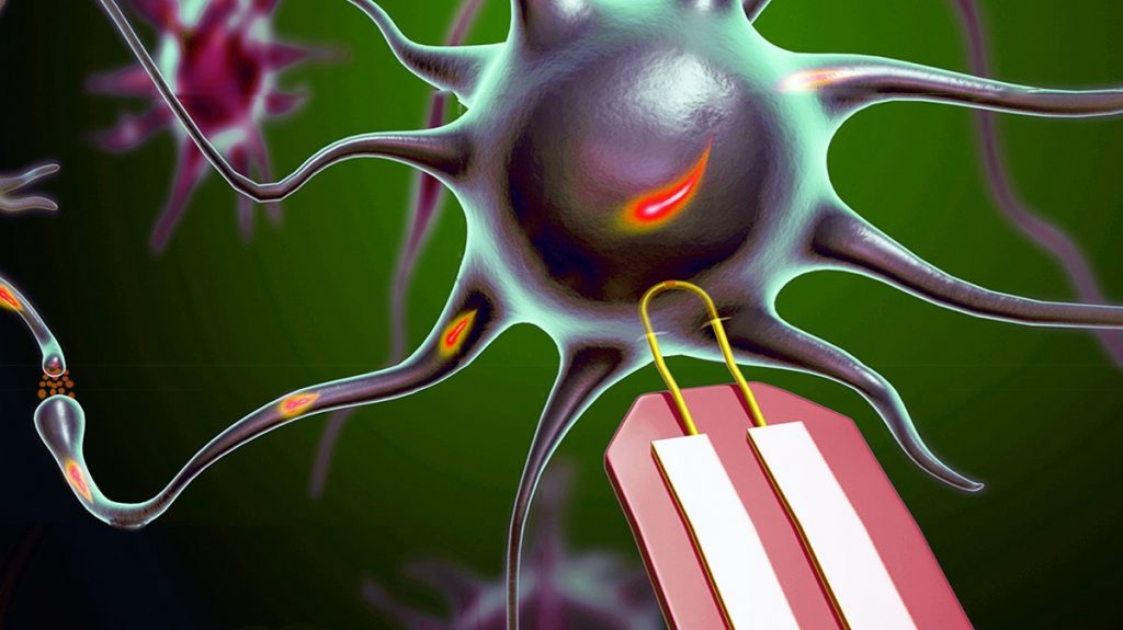
Researchers from the University of Surrey have revealed their new biodegradable motion sensor – paving the way for implanted nanotechnology that could help future sports professionals better monitor their movements to aid rapid improvements, or help caregivers remotely monitor people living with dementia.

A May 21, 12020 University of Surrey press release (also on EurekAlert), which originated the news item, mentioned the collaboration with a South Korean University and provides a few details about this work,

In a paper published by Nano Energy, a team from Surrey’s Advanced Technology Institute (ATI), in partnership with Kyung Hee University in South Korea, detail how they developed a nano-biomedical motion sensor which can be paired with AI systems to recognise movements of distinct body parts.

The ATI’s technology builds on its previous work around triboelectric nanogenerators (TENG), where researchers used the technology to harness human movements and generate small amounts of electrical energy. Combining the two means self-powered sensors are possible without the need for chemical or wired power sources.

In their new research, the team from the ATI developed a flexible, biodegradable and long-lasting TENG from silk cocoon waste. They used a new alcohol treatment technique, which leads to greater durability for the device, even under harsh or humid environments.

Dr. Bhaskar Dudem, project lead and Research Fellow at the ATI, said: “We are excited to show the world the immense potential of our durable, silk film based nanogenerator. It’s ability to work in severe environments while being able to generate electricity and monitor human movements positions our TENG in a class of its own when it comes to the technology.”

Professor Ravi Silva, Director of the ATI, said: “We are proud of Dr Dudem’s work which is helping the ATI lead the way in developing wearable, flexible, and biocompatible TENGs that efficiently harvest environmental energies. If we are to live in a future where autonomous sensing and detecting of pathogens is important, the ability to create both self-powered and wireless biosensors linked to AI is a significant boost.”

Here’s a link to and a citation for the paper,

Exploring theoretical and experimental optimization towards high-performance triboelectric nanogenerators using microarchitecture silk cocoon films by Bhaskar Dudem, R.D. Ishara G. Dharmasena, Sontyana Adonijah Graham, Jung Woo Leem, Harishkumarreddy Patnam, Anki Reddy Mule, S. Ravi P. Silva, Jae Su Yu. Nano Energy DOI: https://doi.org/10.1016/j.nanoen.2020.104882 Available online 11 May 2020, 104882

This paper is behind a paywall.

Human-machine interfaces and ultra-small nanoprobes

We’re back on the cyborg trail or what I sometimes refer to as machine/flesh. A July 3, 2019 news item on ScienceDaily describes the latest attempts to join machine with flesh,

Machine enhanced humans — or cyborgs as they are known in science fiction — could be one step closer to becoming a reality, thanks to new research Lieber Group at Harvard University, as well as scientists from University of Surrey and Yonsei University.

Researchers have conquered the monumental task of manufacturing scalable nanoprobe arrays small enough to record the inner workings of human cardiac cells and primary neurons.

The ability to read electrical activities from cells is the foundation of many biomedical procedures, such as brain activity mapping and neural prosthetics. Developing new tools for intracellular electrophysiology (the electric current running within cells) that push the limits of what is physically possible (spatiotemporal resolution) while reducing invasiveness could provide a deeper understanding of electrogenic cells and their networks in tissues, as well as new directions for human-machine interfaces.

The Lieber Group at Harvard University provided this image illustrating the work,

U-shaped nanowires can record electrical chatter inside a brain or heart cell without causing any damage. The devices are 100 times smaller than their biggest competitors, which kill a cell after recording. Courtesy: University of Surrey

A July 3, 2019 University of Surrey press release (also on EurekAlert), which originated the news item, provides more details about this UK/US/China collaboration,

In a paper published by Nature Nanotechnology, scientists from Surrey’s Advanced Technology Institute (ATI) and Harvard University detail how they produced an array of the ultra-small U-shaped nanowire field-effect transistor probes for intracellular recording. This incredibly small structure was used to record, with great clarity, the inner activity of primary neurons and other electrogenic cells, and the device has the capacity for multi-channel recordings.

Dr Yunlong Zhao from the ATI at the University of Surrey said: “If our medical professionals are to continue to understand our physical condition better and help us live longer, it is important that we continue to push the boundaries of modern science in order to give them the best possible tools to do their jobs. For this to be possible, an intersection between humans and machines is inevitable.

“Our ultra-small, flexible, nanowire probes could be a very powerful tool as they can measure intracellular signals with amplitudes comparable with those measured with patch clamp techniques; with the advantage of the device being scalable, it causes less discomfort and no fatal damage to the cell (cytosol dilation). Through this work, we found clear evidence for how both size and curvature affect device internalisation and intracellular recording signal.”

Professor Charles Lieber from the Department of Chemistry and Chemical Biology at Harvard University said: “This work represents a major step towards tackling the general problem of integrating ‘synthesised’ nanoscale building blocks into chip and wafer scale arrays, and thereby allowing us to address the long-standing challenge of scalable intracellular recording.

“The beauty of science to many, ourselves included, is having such challenges to drive hypotheses and future work. In the longer term, we see these probe developments adding to our capabilities that ultimately drive advanced high-resolution brain-machine interfaces and perhaps eventually bringing cyborgs to reality.”

Professor Ravi Silva, Director of the ATI at the University of Surrey, said: “This incredibly exciting and ambitious piece of work illustrates the value of academic collaboration. Along with the possibility of upgrading the tools we use to monitor cells, this work has laid the foundations for machine and human interfaces that could improve lives across the world.”

Dr Yunlong Zhao and his team are currently working on novel energy storage devices, electrochemical probing, bioelectronic devices, sensors and 3D soft electronic systems. Undergraduate, graduate and postdoc students with backgrounds in energy storage, electrochemistry, nanofabrication, bioelectronics, tissue engineering are very welcome to contact Dr Zhao to explore the opportunities further.

Here’s a link to and a citation for the paper,

Scalable ultrasmall three-dimensional nanowire transistor probes for intracellular recording by Yunlong Zhao, Siheng Sean You, Anqi Zhang, Jae-Hyun Lee, Jinlin Huang & Charles M. Lieber. Nature Nanotechnology (2019) DOI: https://doi.org/10.1038/s41565-019-0478-y Published 01 July 2019

The link I’ve provided leads to a paywall. However, I found a freely accessible version of the paper (this may not be the final published version) here.

Sensing smoke with nanoscale sensors

A Feb. 17, 2015 news item on Nanowerk notes that current smoke sensors are ultra-violet light detectors in the context of research about developing better ones,

Researchers at the University of Surrey’s [UK] Advanced Technology Institute manipulated zinc oxide, producing nanowires from this readily available material to create a ultra-violet light detector which is 10,000 times more sensitive to UV light than a traditional zinc oxide detector.

A Feb. 17, 2015 University of Surrey press release (also on EurekAlert), which originated the news item, provides more detail about the work and the theory (Note: Links have been removed),

Currently, photoelectric smoke sensors detect larger smoke particles found in dense smoke, but are not as sensitive to small particles of smoke from rapidly burning fires.

Researchers believe that this new material could increase sensitivity and allow the sensor to detect distinct particles emitted at the early stages of fires, paving the way for specialist sensors that can be deployed in a number of applications.

“UV light detectors made from zinc oxide have been used widely for some time but we have taken the material a step further to massively increase its performance,” said Professor Ravi Silva, co-author of the study and head of the Advanced Technology Institute. “Essentially, we transformed zinc oxide from a flat film to a structure with bristle-like nanowires, increasing surface area and therefore increasing sensitivity and reaction speed.”

The team predict that the applications for this material could be far-reaching. From fire and gas detection to air pollution monitoring, they believe the sensor could also be incorporated into personal electronic devices – such as phones and tablets – to increase speed, with a response time 1,000 times faster than traditional zinc oxide detectors.

“This is a great example of a bespoke, designer nanomaterial that is adaptable to personal needs, yet still affordable. Due to the way in which this material is manufactured, it is ideally suited for use in future flexible electronics – a hugely exciting area,” added Professor Silva.

Here’s a link to and a citation for the paper,

On-chip Fabrication of High Performance Nanostructured ZnO UV Detectors by Mohammad R. Alenezi, Simon J. Henley, & S. R. P. Silva. Scientific Reports 5, Article number: 8516 doi:10.1038/srep08516 Published 17 February 2015

This paper is open access.

Nanomaterial growth system sold to L’École Polytechnique et L’Universite de Montreal

NanoGrowth-Catalyst produced by Surrey Nanosystems has been sold to L’École Polytechnique de Montréal, the Université de Montréal, and the University of Surrey’s (England) Advanced Technology Institute. From the Jan. 10, 2011 news item on Azonano,

These leading research organisations have chosen the NanoGrowth-Catalyst as a platform for their work on materials including carbon nanotubes, silicon nanowires, graphene and nanoparticles for semiconductor, optical device and other applications. The growth system’s multi-chamber design ensures the purest nanomaterial processing conditions by continuously maintaining the substrate under vacuum, from the deposition of catalysts to growth of materials.

The Advanced Technology Institute (ATI) is a partner to Surrey NanoSystems and has already been using an earlier version of the NanoGrowth system for around four years to support its research into next-generation semiconductor and photonic device technologies. ATI is the first customer to receive the new NanoGrowth-Catalyst, and the system’s advanced processing resources are now starting to play a role in its work. Facilities including the rapid infrared heating process and a water-cooled chuck are helping ATI to grow ordered carbon nanotube (CNT) structures while maintaining the substrate below 350 degrees C. Low temperature processing is critical as CNTs are typically grown at around 700 degrees C – a level that is incompatible with CMOS semiconductor fabrication. This pioneering semiconductor-related work is currently the subject of a current ATI paper in the journal Carbon†.

“The top-down infrared heating technique provided by this tool allows us to localise energy delivery very accurately”, says Professor Ravi Silva, Head of the Nano-Electronics Centre at the Advanced Technology Institute. “The system provides unparalleled control of processing parameters, giving the required flexibility to support research into nanoelectronic materials – including carbon nanotubes, graphene and silicon nanowires – enabling us to overcome roadblocks to ongoing semiconductor development.”

“Some researchers are still relying on simple thermal furnaces to develop nanomaterials”, explains Ben Jensen of Surrey NanoSystems. “The NanoGrowth system’s comprehensive suite of deposition and processing capabilities, plus end-to-end processing in vacuum, gives both researchers and commercial developers precise and automated control over catalyst deposition and material growth, to explore nanomaterial capabilities and turn ideas into repeatable production processes.”

The folks in Montréal will have a special function added to their system (from the news item),

It will also incorporate a unique form of rapid thermal growth for nanomaterials developed to prevent the agglomeration of catalyst particles. The configuration of the tool was specified by Professor Patrick Desjardins, Director of the École Polytechnique’s Department of Engineering Physics.