Tag Archives: Robert Hovden

The nanoscale precision of pearls

An October 21, 2021 news item on phys.org features a quote about nothingness and symmetry (Note: A link has been removed),

In research that could inform future high-performance nanomaterials, a University of Michigan-led team has uncovered for the first time how mollusks build ultradurable structures with a level of symmetry that outstrips everything else in the natural world, with the exception of individual atoms.

“We humans, with all our access to technology, can’t make something with a nanoscale architecture as intricate as a pearl,” said Robert Hovden, U-M assistant professor of materials science and engineering and an author on the paper. “So we can learn a lot by studying how pearls go from disordered nothingness to this remarkably symmetrical structure.” [emphasis mine]

The analysis was done in collaboration with researchers at the Australian National University, Lawrence Berkeley National Laboratory, Western Norway University [of Applied Sciences] and Cornell University.

a. A Keshi pearl that has been sliced into pieces for study. b. A magnified cross-section of the pearl shows its transition from its disorderly center to thousands of layers of finely matched nacre. c. A magnification of the nacre layers shows their self-correction—when one layer is thicker, the next is thinner to compensate, and vice-versa. d, e: Atomic scale images of the nacre layers. f, g, h, i: Microscopy images detail the transitions between the pearl’s layers. Credit: University of Michigan

An October 21, 2021 University of Michigan news release (also on EurekAlert), which originated the news item, reveals a surprise,

Published in the Proceedings of the National Academy of Sciences [PNAS], the study found that a pearl’s symmetry becomes more and more precise as it builds, answering centuries-old questions about how the disorder at its center becomes a sort of perfection. 

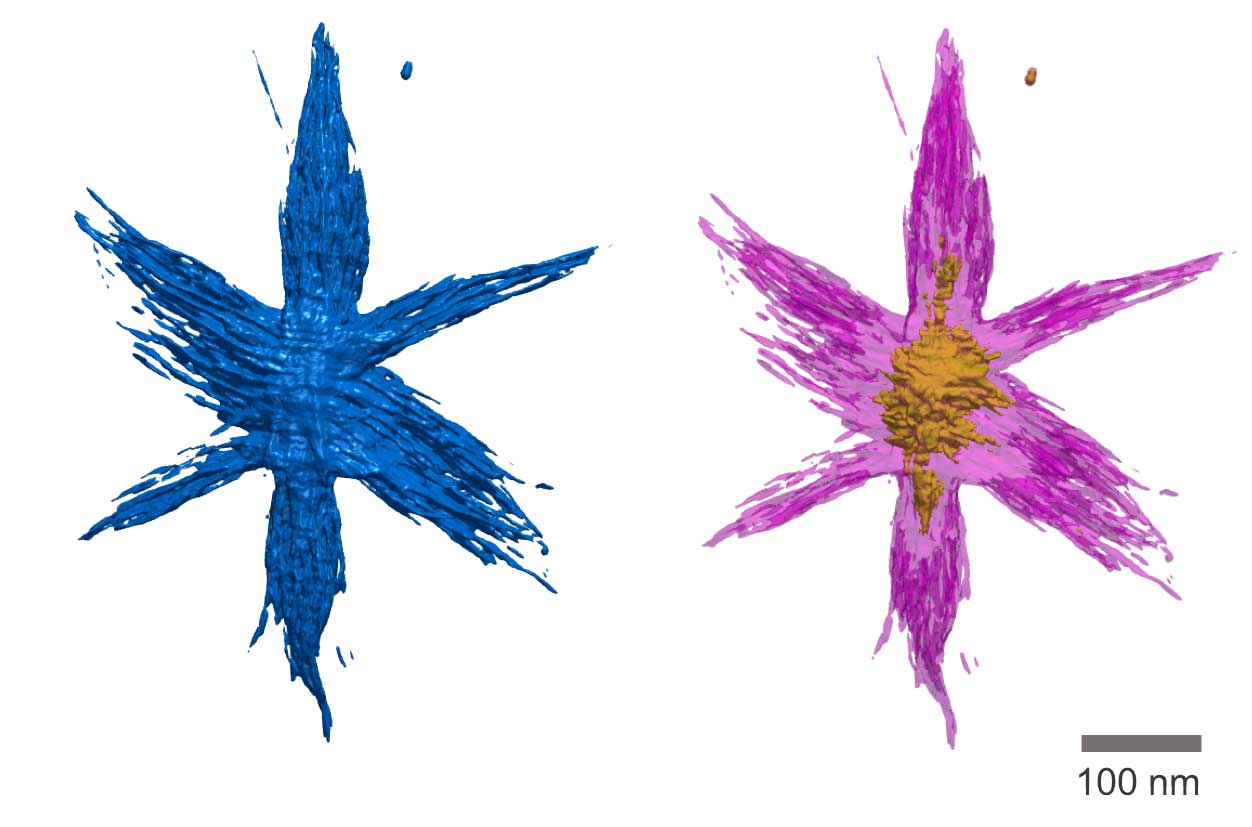
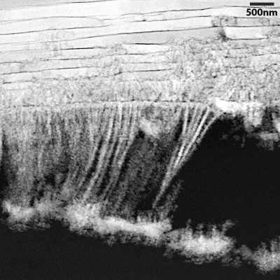
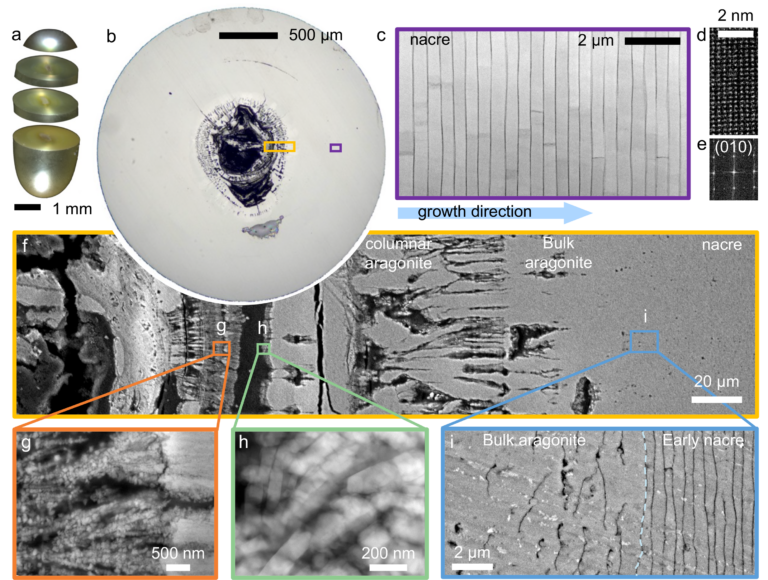
Layers of nacre, the iridescent and extremely durable organic-inorganic composite that also makes up the shells of oysters and other mollusks, build on a shard of aragonite that surrounds an organic center. The layers, which make up more than 90% of a pearl’s volume, become progressively thinner and more closely matched as they build outward from the center.

Perhaps the most surprising finding is that mollusks maintain the symmetry of their pearls by adjusting the thickness of each layer of nacre. If one layer is thicker, the next tends to be thinner, and vice versa. The pearl pictured in the study contains 2,615 finely matched layers of nacre, deposited over 548 days.

“These thin, smooth layers of nacre look a little like bed sheets, with organic matter in between,” Hovden said. “There’s interaction between each layer, and we hypothesize that that interaction is what enables the system to correct as it goes along.”

The team also uncovered details about how the interaction between layers works. A mathematical analysis of the pearl’s layers show that they follow a phenomenon known as “1/f noise,” where a series of events that seem to be random are connected, with each new event influenced by the one before it. 1/f noise has been shown to govern a wide variety of natural and human-made processes including seismic activity, economic markets, electricity, physics and even classical music.

“When you roll dice, for example, every roll is completely independent and disconnected from every other roll. But 1/f noise is different in that each event is linked,” Hovden said. “We can’t predict it, but we can see a structure in the chaos. And within that structure are complex mechanisms that enable a pearl’s thousands of layers of nacre to coalesce toward order and precision.”

The team found that pearls lack true long-range order—the kind of carefully planned symmetry that keeps the hundreds of layers in brick buildings consistent. Instead, pearls exhibit medium-range order, maintaining symmetry for around 20 layers at a time. This is enough to maintain consistency and durability over the thousands of layers that make up a pearl.

The team gathered their observations by studying Akoya “keshi” pearls, produced by the Pinctada imbricata fucata oyster near the Eastern shoreline of Australia. They selected these particular pearls, which measure around 50 millimeters in diameter, because they form naturally, as opposed to bead-cultured pearls, which have an artificial center. Each pearl was cut with a diamond wire saw into sections measuring three to five millimeters in diameter, then polished and examined under an electron microscope.

Hovden says the study’s findings could help inform next-generation materials with precisely layered nanoscale architecture.

“When we build something like a brick building, we can build in periodicity through careful planning and measuring and templating,” he said. “Mollusks can achieve similar results on the nanoscale by using a different strategy. So we have a lot to learn from them, and that knowledge could help us make stronger, lighter materials in the future.”

Here’s a link to and a citation for the paper,

The mesoscale order of nacreous pearls by Jiseok Gim, Alden Koch, Laura M. Otter, Benjamin H. Savitzky, Sveinung Erland, Lara A. Estroff, Dorrit E. Jacob, and Robert Hovden. PNAS vol. 118 no. 42 e2107477118 DOI: https://doi.org/10.1073/pnas.2107477118 Published in issue October 19, 2021 Published online October 18, 2021

This paper appears to be open access.

Using open-source software for a 3D look at nanomaterials

A 3-D view of a hyperbranched nanoparticle with complex structure, made possible by Tomviz 1.0, a new open-source software platform developed by researchers at the University of Michigan, Cornell University and Kitware Inc. Image credit: Robert Hovden, Michigan Engineering

An April 3, 2017 news item on ScienceDaily describes this new and freely available software,

Now it’s possible for anyone to see and share 3-D nanoscale imagery with a new open-source software platform developed by researchers at the University of Michigan, Cornell University and open-source software company Kitware Inc.

Tomviz 1.0 is the first open-source tool that enables researchers to easily create 3-D images from electron tomography data, then share and manipulate those images in a single platform.

A March 31, 2017 University of Michigan news release, which originated the news item, expands on the theme,

The world of nanoscale materials—things 100 nanometers and smaller—is an important place for scientists and engineers who are designing the stuff of the future: semiconductors, metal alloys and other advanced materials.

Seeing in 3-D how nanoscale flecks of platinum arrange themselves in a car’s catalytic converter, for example, or how spiky dendrites can cause short circuits inside lithium-ion batteries, could spur advances like safer, longer-lasting batteries; lighter, more fuel efficient cars; and more powerful computers.

“3-D nanoscale imagery is useful in a variety of fields, including the auto industry, semiconductors and even geology,” said Robert Hovden, U-M assistant professor of materials science engineering and one of the creators of the program. “Now you don’t have to be a tomography expert to work with these images in a meaningful way.”

Tomviz solves a key challenge: the difficulty of interpreting data from the electron microscopes that examine nanoscale objects in 3-D. The machines shoot electron beams through nanoparticles from different angles. The beams form projections as they travel through the object, a bit like nanoscale shadow puppets.

Once the machine does its work, it’s up to researchers to piece hundreds of shadows into a single three-dimensional image. It’s as difficult as it sounds—an art as well as a science. Like staining a traditional microscope slide, researchers often add shading or color to 3-D images to highlight certain attributes.

A 3-D view of a particle used in a hydrogen fuel cell powered vehicle. The gray structure is carbon; the red and blue particles are nanoscale flecks of platinum. The image is made possible by Tomviz 1.0. Image credit: Elliot Padget, Cornell UniversityA 3-D view of a particle used in a hydrogen fuel cell powered vehicle. The gray structure is carbon; the red and blue particles are nanoscale flecks of platinum. The image is made possible by Tomviz 1.0. Image credit: Elliot Padget, Cornell UniversityTraditionally, they’ve have had to rely on a hodgepodge of proprietary software to do the heavy lifting. The work is expensive and time-consuming; so much so that even big companies like automakers struggle with it. And once a 3-D image is created, it’s often impossible for other researchers to reproduce it or to share it with others.

Tomviz dramatically simplifies the process and reduces the amount of time and computing power needed to make it happen, its designers say. It also enables researchers to readily collaborate by sharing all the steps that went into creating a given image and enabling them to make tweaks of their own.

“These images are far different from the 3-D graphics you’d see at a movie theater, which are essentially cleverly lit surfaces,” Hovden said. “Tomviz explores both the surface and the interior of a nanoscale object, with detailed information about its density and structure. In some cases, we can see individual atoms.”

Key to making Tomviz happen was getting tomography experts and software developers together to collaborate, Hovden said. Their first challenge was gaining access to a large volume of high-quality tomography. The team rallied experts at Cornell, Berkeley Lab and UCLA to contribute their data, and also created their own using U-M’s microscopy center. To turn raw data into code, Hovden’s team worked with open-source software maker Kitware.

With the release of Tomviz 1.0, Hovden is looking toward the next stages of the project, where he hopes to integrate the software directly with microscopes. He believes that U-M’s atom probe tomography facilities and expertise could help him design a version that could ultimately uncover the chemistry of all atoms in 3-D.

“We are unlocking access to see new 3D nanomaterials that will power the next generation of technology,” Hovden said. “I’m very interested in pushing the boundaries of understanding materials in 3-D.”

There is a video about Tomviz,

You can download Tomviz from here and you can find Kitware here. Happy 3D nanomaterial viewing!

Creating multiferroic material at room temperature

A Sept. 23, 2016 news item on ScienceDaily describes some research from Cornell University (US),

Multiferroics — materials that exhibit both magnetic and electric order — are of interest for next-generation computing but difficult to create because the conditions conducive to each of those states are usually mutually exclusive. And in most multiferroics found to date, their respective properties emerge only at extremely low temperatures.

Two years ago, researchers in the labs of Darrell Schlom, the Herbert Fisk Johnson Professor of Industrial Chemistry in the Department of Materials Science and Engineering, and Dan Ralph, the F.R. Newman Professor in the College of Arts and Sciences, in collaboration with professor Ramamoorthy Ramesh at UC Berkeley, published a paper announcing a breakthrough in multiferroics involving the only known material in which magnetism can be controlled by applying an electric field at room temperature: the multiferroic bismuth ferrite.

Schlom’s group has partnered with David Muller and Craig Fennie, professors of applied and engineering physics, to take that research a step further: The researchers have combined two non-multiferroic materials, using the best attributes of both to create a new room-temperature multiferroic.

Their paper, “Atomically engineered ferroic layers yield a room-temperature magnetoelectric multiferroic,” was published — along with a companion News & Views piece — Sept. 22 [2016] in Nature. …

A Sept. 22, 2016 Cornell University news release by Tom Fleischman, which originated the news item, details more about the work (Note: A link has been removed),

The group engineered thin films of hexagonal lutetium iron oxide (LuFeO3), a material known to be a robust ferroelectric but not strongly magnetic. The LuFeO3 consists of alternating single monolayers of lutetium oxide and iron oxide, and differs from a strong ferrimagnetic oxide (LuFe2O4), which consists of alternating monolayers of lutetium oxide with double monolayers of iron oxide.

The researchers found, however, that they could combine these two materials at the atomic-scale to create a new compound that was not only multiferroic but had better properties that either of the individual constituents. In particular, they found they need to add just one extra monolayer of iron oxide to every 10 atomic repeats of the LuFeO3 to dramatically change the properties of the system.

That precision engineering was done via molecular-beam epitaxy (MBE), a specialty of the Schlom lab. A technique Schlom likens to “atomic spray painting,” MBE let the researchers design and assemble the two different materials in layers, a single atom at a time.

The combination of the two materials produced a strongly ferrimagnetic layer near room temperature. They then tested the new material at the Lawrence Berkeley National Laboratory (LBNL) Advanced Light Source in collaboration with co-author Ramesh to show that the ferrimagnetic atoms followed the alignment of their ferroelectric neighbors when switched by an electric field.

“It was when our collaborators at LBNL demonstrated electrical control of magnetism in the material that we made that things got super exciting,” Schlom said. “Room-temperature multiferroics are exceedingly rare and only multiferroics that enable electrical control of magnetism are relevant to applications.”

In electronics devices, the advantages of multiferroics include their reversible polarization in response to low-power electric fields – as opposed to heat-generating and power-sapping electrical currents – and their ability to hold their polarized state without the need for continuous power. High-performance memory chips make use of ferroelectric or ferromagnetic materials.

“Our work shows that an entirely different mechanism is active in this new material,” Schlom said, “giving us hope for even better – higher-temperature and stronger – multiferroics for the future.”

Collaborators hailed from the University of Illinois at Urbana-Champaign, the National Institute of Standards and Technology, the University of Michigan and Penn State University.

Here is a link and a citation to the paper and to a companion piece,

Atomically engineered ferroic layers yield a room-temperature magnetoelectric multiferroic by Julia A. Mundy, Charles M. Brooks, Megan E. Holtz, Jarrett A. Moyer, Hena Das, Alejandro F. Rébola, John T. Heron, James D. Clarkson, Steven M. Disseler, Zhiqi Liu, Alan Farhan, Rainer Held, Robert Hovden, Elliot Padgett, Qingyun Mao, Hanjong Paik, Rajiv Misra, Lena F. Kourkoutis, Elke Arenholz, Andreas Scholl, Julie A. Borchers, William D. Ratcliff, Ramamoorthy Ramesh, Craig J. Fennie, Peter Schiffer et al. Nature 537, 523–527 (22 September 2016) doi:10.1038/nature19343 Published online 21 September 2016

Condensed-matter physics: Multitasking materials from atomic templates by Manfred Fiebig. Nature 537, 499–500  (22 September 2016) doi:10.1038/537499a Published online 21 September 2016

Both the paper and its companion piece are behind a paywall.

Clues as to how mother of pearl is made

Iridescence seems to fascinate scientists and a team at Cornell University is no exception (from a Dec. 4, 2015 news item on Nanowerk),

Mother nature has a lot to teach us about how to make things.

With that in mind, Cornell researchers have uncovered the process by which mollusks manufacture nacre – commonly known as “mother of pearl.” Along with its iridescent beauty, this material found on the insides of seashells is incredibly strong. Knowing how it’s made could lead to new methods to synthesize a variety of new materials with as yet unguessed properties.

“We have all these high-tech facilities to make new materials, but just take a walk along the beach and see what’s being made,” said postdoctoral research associate Robert Hovden, M.S. ’10, Ph.D. ’14. “Nature is doing incredible nanoscience, and we need to dig into it.”

A Dec. 4, 2015 Cornell University news release by Bill Steele, which originated the news item, expands on the theme,

Using a high-resolution scanning transmission electron microscope (STEM), the researchers examined a cross section of the shell of a large Mediterranean mollusk called the noble pen shell or fan mussel (Pinna nobilis). To make the observations possible they had to develop a special sample preparation process. Using a diamond saw, they cut a thin slice through the shell, then in effect sanded it down with a thin film in which micron-sized bits of diamond were embedded, until they had a sample less than 30 nanometers thick, suitable for STEM observation. As in sanding wood, they moved from heavier grits for fast cutting to a fine final polish to make a surface free of scratches that might distort the STEM image.

Images with nanometer-scale resolution revealed that the organism builds nacre by depositing a series of layers of a material containing nanoparticles of calcium carbonate. Moving from the inside out, these particles are seen coming together in rows and fusing into flat crystals laminated between layers of organic material. (The layers are thinner than the wavelengths of visible light, causing the scattering that gives the material its iridescence.)

Exactly what happens at each step is a topic for future research. For now, the researchers said in their paper, “We cannot go back in time” to observe the process. But knowing that nanoparticles are involved is a valuable insight for materials scientists, Hovden said.

Here’s an image from the researchers,

Electron microscope image of a cross-section of a mollusk shell. The organism builds its shell from the inside out by depositing layers of calcium carbonate nanoparticles. As the particle density increases over time they fuse into large flat crystals embedded in layers of organic material to form nacre. Courtesy: Cornell University

Electron microscope image of a cross-section of a mollusk shell. The organism builds its shell from the inside out by depositing layers of calcium carbonate nanoparticles. As the particle density increases over time they fuse into large flat crystals embedded in layers of organic material to form nacre. Courtesy: Cornell University

Here’s a link to and a citation for the paper,

Nanoscale assembly processes revealed in the nacroprismatic transition zone of Pinna nobilis mollusc shells by Robert Hovden, Stephan E. Wolf, Megan E. Holtz, Frédéric Marin, David A. Muller, & Lara A. Estroff. Nature Communications 6, Article number: 10097 doi:10.1038/ncomms10097 Published 03 December 2015

This is an open access paper.

Art and nanotechnology at Cornell University’s (US) 2014 Biennial/Biennale

The 2014 Cornell [University located in New York State, US] Council for the Arts (CCA) Biennial, “Intimate Cosmologies: The Aesthetics of Scale in an Age of Nanotechnology” was announced in a Dec. 5, 2013 news item on Nanowerk,

A campuswide exhibition next fall will explore the cultural and human consequences of seeing the world at the micro and macro levels, through nanoscience and networked communications.

From Sept. 15 to Dec. 22, the 2014 Cornell Council for the Arts (CCA) Biennial, “Intimate Cosmologies: The Aesthetics of Scale in an Age of Nanotechnology”, will feature several events and principal projects by faculty and student investigators and guest artists – artist-in-residence kimsooja, Trevor Paglen and Rafael Lozano-Hemmer – working in collaboration with Cornell scientists and researchers.

The Dec.5, 2013 Cornell University news release written by Daniel Aloi, which originated the news item, describes the plans for and events leading to the biennale in Fall 2014,

The inaugural biennial theme was chosen to frame dynamic changes in 21st-century culture and art practice, and in nanoscale technology. The multidisciplinary initiative intends to engage students, faculty and the community in demonstrations of how radical shifts in scale have become commonplace, and how artists address realms of human experience lying beyond immediate sensory perception.

“Participating in the biennial is very exciting. We’re engaging the idea of nano and investigating scale as part of the value of art in performance,” said Beth Milles ’88, associate professor in the Department of Performing and Media Arts, who is collaborating on a project with students and with artist Lynn Tomlinson ’88.

A series of events and curricula this fall and spring are preceding the main Biennial exhibition. Joe Davis and Nathaniel Stern ’99 presented talks this semester, and CCA will bring Paul Thomas, Stephanie Rothenberg, Ana Viseu and others to campus in the coming months.

kimsooja, an acclaimed multimedia artist in performance, video and installation, addresses issues of the displaced self and recently represented Korea in the 55th Venice Biennale. She visited the campus Nov. 22-23 to meet with Uli Weisner and students from his research group, who will work with her to realize her large-scale installation here next fall.

Lozano-Hemmer has worked on both ends of the scale spectrum, from laser-etched poetry on human hairs to an interactive light sculpture over Mexico City, Toronto and Yamaguchi, Japan. Paglen’s researched-based work blurs lines between science, contemporary art, journalism and other disciplines.

The Biennial focus brings together artists and scientists who share a common curiosity regarding the position of the individual within the larger world, CCA Director Stephanie Owens said.

“Scientists are suddenly designers creating new forms,” she said. “And artists are increasingly interested in how things are structured, down to the biological level. Both are designing and discovering new ways of synthesizing natural properties of the material world with the fabricated experiences that extend and express the impact of these properties on our lives.”

Here’s a sample of the work that will be featured at the Biennale,

A prototype image of architecture professor Jenny Sabin's "eSkin" CCA Biennial project, an interactive simulation of a building façade that behaves like a living organism. Credit: Jenny Sabin Courtesy: Cornell University

A prototype image of architecture professor Jenny Sabin’s “eSkin” CCA Biennial project, an interactive simulation of a building façade that behaves like a living organism. Credit: Jenny Sabin Courtesy: Cornell University

Aloi includes a description of some of the exhibits and shows to be featured,

 The principal projects to be presented are:

  • “eSkin” – Architecture professor Jenny Sabin addresses ecology and sustainability issues with buildings that behave like organisms. Her project is an interactive simulation of a façade material incorporating nano- and microscale substrates plated with human cells.
  • “Nano Performance: In 13 Boxes” – Performing and media arts professor Beth Milles ‘88, animator/visual artist Lynn Tomlinson ‘88 and students from different majors will collaborate on 13 media installations and live performances situated across campus. Computer mapping and clues linking the project’s components will assist in “synthesizing the 13 events as a whole experience – it has a lot to do with discovering the performance,” Mills said.
  • “Nano Where: Gas In, Light Out” – Juan Hinestroza, fiber science, and So-Yeon Yoon, design and environmental analysis, will demonstrate the potential of molecular-level metal-organic frameworks as wearable sensors to detect methane and poisonous gases, using a sealed gas chamber and 3-D visual art.
  • “Paperscapes” – Three architecture students – teaching associate Caio Barboza ’13; Joseph Kennedy ’15 and Sonny Xu ’13 – will render the microscopic textures of a sheet of paper as a 3-D inhabitable landscape.
  • “When Art Exceeds Perception” – Ph.D. student in applied physics Robert Hovden will explore replication and plagiarism in nanoscale reproductions, 1,000 times smaller than the naked eye can see, of famous works of art inscribed onto a silicon crystal.

The Cornell Council for the Arts (CCA) has more information about their 2014 ‘nano Biennale’ here. This looks very exciting and I wish I could be there.

One final note, I’ve used the Biennale rather than Biennial as I associate Biennial and the US with the dates of 1776 and 1976 when the country celebrated its 200th anniversary.