Monthly Archives: August 2013

Table salt, acting as a heat scavenger, enables cheaper silicon nanostructures

Recyclable, easily obtained, and inexpensive, there’s a magic ingredient which could make producing silicon nanostructures easier and cheaper according an Aug. 8, 2013 news item on Nanowerk,

Chemists at Oregon State University have identified a compound that could significantly reduce the cost and potentially enable the mass commercial production of silicon nanostructures – materials that have huge potential in everything from electronics to biomedicine and energy storage.

This extraordinary compound is called table salt.

The Aug. 8, 2013 Oregon State University news release, which originated the news item, describes the principle at work and possible applications for the technique,

By melting and absorbing heat at a critical moment during a “magnesiothermic reaction,” the salt prevents the collapse of the valuable nanostructures that researchers are trying to create. The molten salt can then be washed away by dissolving it in water, and it can be recycled and used again.

The concept, surprising in its simplicity, should open the door to wider use of these remarkable materials that have stimulated scientific research all over the world.

“This could be what it takes to open up an important new industry,” said David Xiulei Ji, an assistant professor of chemistry in the OSU College of Science. “There are methods now to create silicon nanostructures, but they are very costly and can only produce tiny amounts.

“The use of salt as a heat scavenger in this process should allow the production of high-quality silicon nanostructures in large quantities at low cost,” he said. “If we can get the cost low enough many new applications may emerge.”

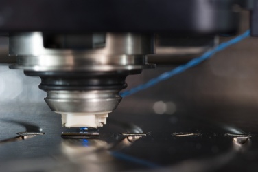
Silicon, the second most abundant element in the Earth’s crust, has already created a revolution in electronics. But silicon nanostructures, which are complex structures much smaller than a speck of dust, have potential that goes far beyond the element itself.

Uses are envisioned in photonics, biological imaging, sensors, drug delivery, thermoelectric materials that can convert heat into electricity, and energy storage.

Batteries are one of the most obvious and possibly first applications that may emerge from this field, Ji said. It should be possible with silicon nanostructures to create batteries – for anything from a cell phone to an electric car – that last nearly twice as long before they need recharging.

Existing technologies to make silicon nanostructures are costly, and simpler technologies in the past would not work because they required such high temperatures. Ji developed a methodology that mixed sodium chloride and magnesium with diatomaceous earth, a cheap and abundant form of silicon.

When the temperature reached 801 degrees centigrade, the salt melted and absorbed heat in the process. This basic chemical concept – a solid melting into a liquid absorbs heat – kept the nanostructure from collapsing.

The sodium chloride did not contaminate or otherwise affect the reaction, researchers said. Scaling reactions such as this up to larger commercial levels should be feasible, they said.

The study also created, for the first time with this process, nanoporous composite materials of silicon and germanium. These could have wide applications in semiconductors, thermoelectric materials and electrochemical energy devices.

Here’s a link to and a citation for the published paper,

Efficient Fabrication of Nanoporous Si and Si/Ge Enabled by a Heat Scavenger in Magnesiothermic Reactions by Wei Luo, Xingfeng Wang, Colin Meyers, Nick Wannenmacher, Weekit Sirisaksoontorn, Michael M. Lerner & Xiulei Ji. Scientific Reports 3, Article number: 2222 doi:10.1038/srep02222 Published 17 July 2013

This article is open access.

GreenCentre Canada births Precision Molecular Design Corporation

An Aug. 9, 2013 news item on Azonano features Ontario Network of Excellence (ONE) member, Centre of Excellence for Commercialization and Research (CECR) member, and business incubator, GreenCentre Canada,

GreenCentre Canada has recently incorporated its third spinoff company, Precision Molecular Design Corporation. Based on a technology invented at Carleton University, Precision Molecular Design’s proprietary ALD precursors enable “greener” production of smaller and faster microchips for the semiconductor industry.

The Aug. 8, 2013 GreenCentre Canada news release, which originated the news item, describes the innovation and the new company,

Precision Molecular Design’s breakthrough metal deposition technology allows manufacturers to generate circuit interconnects in successive layers one atom at a time. This will allow the semiconductor industry to develop the next generation of smaller microchips, ushering in new miracles of miniaturization. The technology will also enable the production of microchips with less waste and lower power consumption. For the consumer, this means longer battery life, more convenient sizing, less heat generation and a reduced carbon footprint.
Invented by Professor Sean Barry of Carleton, GreenCentre originally supported this breakthrough ALD technology with proof-of-principle funding of $16,000 and, in 2011, in-licensed the technology for continued commercial development. In 2012, GreenCentre licensed the technology to Digital Specialty Chemicals, a fine chemical manufacturer, to develop an industrial process to manufacture the precursors.

Precision Molecular is now looking for investors and partners for their precursors and offer development and contract services for the development of materials and processes for the ALD market.

Launched in July 2013, the Precision Molecular Design website is here.

As for its progenitor, GreenCentre Canada, here’s a little more about the organization from its About Us page (Note: Links have been removed),

Formed in 2009 and funded by the governments of Ontario and Canada, and industry, GreenCentre is a member of the Ontario Network of Excellence (ONE) and the Centres of Excellence for Commercialization and Research (CECR).  GreenCentre’s product and application development activities are housed in a 10,000 square foot facility dominated by state-of-the-art web labs with solvent-handling systems, inert atmosphere glove boxes and standard analytical equipment. GreenCentre is located at Innovation Park at Queen’s University in Kingston, Ontario, Canada.

The organization’s main focus is on developing green chemistry solutions and, presumably, new businesses.

Graphene bits from the UK’s National Physical Laboratory and Cientifica

In the first bit of this week’s graphene news, the UK”s National Physical Laboratory (NPL) has joined the Graphene Stakeholders Association according to an Aug. 5, 2013 NPL news release,

The National Physical Laboratory (NPL) has joined the Graphene Stakeholders Association (GSA) as a lifetime member. NPL will work closely with the GSA to promote the responsible development of graphene and graphene-enabled technologies and applications.

“We foresee a significant role for NPL in the GSA in helping to develop common and accepted nomenclature, definitions, standard metrology and testing methods that will help foster and facilitate the development of graphene and graphene-enabled applications globally,” stated GSA co-founder, Stephen Waite. “We are delighted with NPL’s decision to join the GSA and look forward to working closely with Andrew Pollard and his colleagues in the months and years ahead,” says Waite.

NPL’s Andrew Pollard, who joins the GSA’s Advisory Board, said: “NPL has a leading role in the development of measurement techniques and international standards for graphene and 2-D materials, and the formation of the GSA is extremely well-timed as graphene progresses from the research laboratory to commercialisation. This partnership between two organisations with such well-aligned aims should enable the widely-predicted growth of a global graphene industry.”

I mentioned the founding of the Graphene Stakeholders Association in an April 23, 2013 posting. At the time I noted the group’s very interesting Graphene Industry Information page, which features these tidbits,

China has published more graphene patents than any other country, at 2,204, ahead of 1,754 for the U.S., 1,160 for South Korea, and 54 for the U.K.

South Korea’s Samsung has more graphene patents than any single company.

Nokia is part of the 74-company Graphene Flagship Consortium that is receiving a €1 billion ($1.35 billion) grant that the E.U. announced in January 2013.

Nokia, Philips, U.K. invention stalwart Dyson, weapons and aerospace company BAE Systems, and others have committed £13 million ($20.5 million) to a graphene development center [Cambridge Graphene Centre as per my Jan. 24, 2013 posting] at Cambridge University, to go along with £12 million ($18.9 million) from the British government. [Also, there’s a new National Graphene Institute being built in Manchester, UK {my Jan. 14, 2013 posting}.]

….

Graphene is prohibitively expensive to make today. As recently as 2008, it cost $100 million to produce a single cubic centimeter of graphene.

Researchers are working on methods to reduce the cost of manufacturing and help make graphene a ubiquitous fabrication material.

Graphene film companies face major commercialization hurdles, including reducing costs, scaling-up the substrate transfer process, overcoming current deposition area limitations, and besting other emerging material solutions.

This leads to the 2nd bit of graphene news, Cientifica (a business consultancy focusing on emerging technologies) has released its Graphene Opportunity Report, from the report’s webpage (Note: Links have been removed),

A decade ago when we published the first edition of the Nanotechnology Opportunity Report, there were predictions of untold riches for early investors, the replacement of all manufacturing as we know it, and the mythical trillion-dollar market.

Cientifica went against the grain by predicting that it would be hard for anyone to make money from nanomaterials, and that the real value would be in the applications. This has been borne out by the failure of even large global companies such as Mitsubishi Chemical and Bayer to make much headway with fullerenes and carbon nanotubes, and the failure of countless smaller nanomaterials producers.

On the other hand companies making use of nanomaterials, Germany’s Magforce Technologies and the US based BIND Therapeutics have shown what can be achieved when nanomaterials are applied to large addressable markets, in this case drug delivery.

Is Graphene The New Nanotech?

A similar amount of hype currently surrounds graphene, with wild predictions of applications ranging from microelectronics to water
treatment. This report examines these claims and taking the rational approach for which Cientifica is known, considers how valid these are and evaluates the chances of success.

We also look in detail at the graphene producers. Graphene comes in a wide range of forms, each with its own particular set of addressable applications. No one producer covers all applications and many are destined to be niche players. As with nanomaterials, many companies currently producing graphene are destined to burn brightly and then be unceremoniously snuffed out when scale up or access to applications fails to materialise.

..

As with all Cientifica reports, we look beyond the hype and take a rational and dispassionate look at the entire graphene value chain, from graphite to THz electronics. There will be long-term winners, and we indicate what strategies are required to join this small elite band, and we provide a wealth of lessons from our previous experience in nanotechnologies and life sciences.

Most importantly, we look beyond the narrow graphene or nanotechnology worlds and assess graphene’s chances of success in competing with a wide range of other technologies, many of which have not been considered by those concentrating solely on graphene.

The Graphene Opportunity Report is available at GBP 2000/EUR 2300/USD 3000.

You can access the report’s Table of Contents here.

Thailand’s NANOTEC celebrates10th anniversary

Congratulations to Thailand’s NANOTEC (National Nanotechnology Center) on reaching its 10th anniversary. According to an Aug. 7, 2013 news item on Nanowerk, the center was founded on Aug. 13, 2003,

Ten years have gone by quickly proving the saying that “time and tide wait for no man”. It was on August 13, 2003 that the Thai government approved the setup of the National Nanotechnology Center (NANOTEC) under National Science and Technology Development Agency (NSTDA),

Sirirurg Songsivilai, M.D.,Ph.D,NANOTEC Executive Director, provides an overview of the last 10 years and some hints about future prospects in his About Us message,

NANOTEC has come a long way since then and several accomplishments have come to bear. In the area of human resource, NANOTEC have successfully up its research pool to over 100 researchers and assistant researchers, carrying out research at our headquarters at Thailand Science Park. This is equivalent to 70% of the total NANOTEC staff. With regards to publication, NANOTEC researchers have published a total of 357 international publications. This is considered a significant number given our researcher pool.

NANOTEC research highlights have been forth coming in the last few years. This is normal as research projects takes time to complete. Some of the highlight projects include the SOS mobile water purification unit, the nano cosmeceutical QAcne pad made from encapsulation of mangosten extract, the Nano Bednet which contain nano scale long-lasting formulation of mosquito-insecticide, nano functional fabrics, controlled release fertilizer, and smart soil made from water hyacinth.

The last ten years have also seen an increase in the number of collaborative partnerships both local and international. The establishment of the Center of Excellence in Nanotechnology (COEs) with 8 leading Thai universities continues to help us leap frog our research initiatives. These partnerships have greatly helped to broaden our look on research from global aspects. NANOTEC also established strategic alliance with international nanotechnology centers and is playing leading role as one of the world-leading institutes.

So, what is in store for NANOTEC in the coming 10 years? We will continue to concentrate our focus on R&D programs that will have impacts. In order to do this, we will initiate the Flagship program approach in which all researchers are encouraged to participate. ….

You can find out more about NANOTEC and its current doings on its homepage.

News about Canadian Science Policy Conference 2013 and Science Borealis logo contest

The Canadian Science Policy Conference 2013 organizers have announced their preliminary programme and early  registration for the 2013 (5th annual) conference, from an Aug. 8, 2013 announcement,

The 5th Canadian Science Policy Conference

Registration is Now Open and Panels are announced below.

After 5 years, the Canadian Science Policy Conference (CSPC) is returning to Toronto to host an expanded, diversified, richer science policy conference. The conference offers a unique platform for stakeholders to connect at the national level, to exchange ideas on key issues in science, technology, and innovation policy, and to craft a future based on strong, dynamic, and innovative policy-making for the benefit of all Canadians.

CSPC 2013 Highlights:

  • 400+ participants
  • 3 pre-conference workshop symposiums (Science Policy Nuts and Bolts, Science Diplomacy & Science and Technology Communication)
  • Inauguration of the Awards of Excellence in Science Policy – a first in Canada
  • Double the number of sessions from last year, now up to 30
  • Diversified panel sessions maximizing panelist-participant interactions

….

We are pleased to announce 25 panels across CSPC 2013’s five themes: international trade and diplomacy, private sector innovation, communicating science, graduate studies and training, and emerging issues in Canadian science policy.

Asian Science and Technology Strategies and Process – Implications for Canada

Asia Pacific Foundation of Canada

The evolving science and technology landscape for development in the South and the models and opportunities for science diplomacy

International Development Research Centre

The world in 2020: Three questions for internationalized science

UK Science & Innovation Network

The complexity of driving the bio-economy: Genomics, Canada’s natural resources and private-public collaborations

Genome Canada
Canada’s Commercialization Challenge

Schroeder & Schroeder Inc

Inspiring Excellence – Engaging students in meaningful science experiences

Let’s Talk Science
The Solitudes: Government science, the Media, and Those who help them Interact: Can we ever get along under today’s rules of engagement?

Canadian Science Writers’ Association

Journalists are from Mars; scientists are from Venus. Will they ever be on the same planet?

Maclean’s/Medical Post/MIT

Who are the innovators in Canada and what do we know about the individuals who drive innovation?

THECIS

Evaluating large-scale S&T initiatives: A case study on the complexity of capturing and disseminating meaningful outcome and impacts data

Genome Canada 

Science Funding Mechanisms

Samuel Lunenfeld Research Institute
Science blogging in Canada: Making use of a valuable resource [emphasis mine]

Science Communications Canada
Training the next generation of scientists – who are they and what will they do?

Canadian Association of Postdoctoral Scholars and The Black Hole Blog
Is a PhD Really a Waste of Time?

University of Toronto
Is Canada able to meet its needs for research and innovation on northern issues, given that it does not have graduate programs situated in the three Canadian territories?

Government of Yukon
Strategies to Enhance Productivity of Knowledge Workers

Strategy First Consulting (SFC) 

Ocean Research and Policy

Ocean Networks Canada 

Canadian Innovation: Understanding the role of IR&D

The Council of Canadian Academies

Big data: solutions for the big problems faced by modern societies

British Consulate General Toronto 

More details about the program will be posted on our website shortly. The titles of six more panels will also be announced at this time.

I have a little inside scoop about the panel on science blogging.  One of the panelists (I believe she proposed the presentation) is Sarah Boon of the Watershed Moments blog who has also been one of the prime movers behind the Science Borealis initiative.

I last wrote about Science Borealiis (blogging science from Canadian perspectives) and its logo contest in a June 14, 2013 posting, which mentioned the other prime movers behind this science aggregator/hub/community along with details about the contest. For anyone interested in making a submission, the contest deadline was extended to Aug. 15, 2013.

Recently, we (I’m involved too) announced the contest jurors,

The logos will be judged by

  • Raymond K. Nakamura, science blogger (Vancouver’s Science World blog), web comic artist, and science exhibition content developer (http://raymondsbrain.com/)
  • Janice Whitehead, owner and publisher of Preview: The Gallery Guide, a visual arts publication that is distributed through Alberta, BC, Washington state, and Oregon (http://www.preview-art.com/)

There are prizes,

  • Prizes will be awarded to 3 finalists chosen by the Science Borealis team. Prizes will be awarded as follows.
    • Winners:
    • Personal subscription to any NRC Research Press journal (published by Canadian Science Publishing), plus a $50 amazon gift card and a laptop bag
    • Runners Up:
    • {Prizes provided by Genome Alberta and Canadian Science Publishing}
  • Finalists will be announced via Science Borealis social media channels
  • Finalists’ designs will not be revealed publicly
  • The winning design and designer will be announced via Science Borealis social media channels
  • The winning designer will be recognized on the Science Borealis website with a link to his/her site if applicable

Good luck to all and, should you be attending the Canadian Science Policy Conference, please don’t miss the science blogging panel.

Comparing US and German reception of nanotechnology

There’s a tv (television) newsmagazine show devoted to nanotechnology that’s broadcast amongst other news shows in Germany according to an Aug. 8, 2013 news item on Azonano,

As Paul Youngman, professor of German at Washington and Lee (W&L) University, and student researchers Matthew Bittner and Curtis Correll learned this summer, your perception of nanotechnology—the manipulation of extremely small particles to make materials and machines—may depend on where you live.

In Germany, the scientific newsmagazine Nano spotlights nanoscience and emerging technologies. The show airs alongside other news programs. [emphasis mine] In the U.S., nanoscience is not featured regularly in the news. When U.S. broadcasters do run nanoscience stories, the coverage tends to be more sensational, said Bittner, whose research was funded by the W&L German Department.

“The Germans will look more at the short-term effect of science and technology—more realistic expectations,” said Bittner. American shows, while realistic, tend to look further into the future, and they highlight the most breathtaking possibilities.

The Aug. 7, 2013 W&L press release by Jeff Hanna, which originated the news item, notes that Youngman’s research is providing the basis for a forthcoming book,

“Nanotechnology is an emerging science that we don’t completely have a handle on, and our premise is always that science is never divorced from the larger culture at hand,” said Youngman. “What we’re doing is analyzing the cultural reception of nanotechnology as it exists right now. It’s a comparative study between German and U.S. reception.”

Rhetoric and public perception affect how nanotechnology is funded and regulated. Youngman’s book-in-progress, “National Nanotechnologies: Nanodiscourse in Germany and the United States,” compares rhetoric from a variety of sources in both countries. The book also examines nano imagery.

He focuses on Germany and the U.S. because they are the largest investors in nanoscience and technology (NST) in the European Union and North America, and the countries have partnered on numerous commercial and academic NST endeavors. Youngman is collaborating with Ljiljana Fruk, group leader at the Center for Functional Nanostructures (CFN) in Karlsruhe, Germany.

As noted in the press release, Youngman’s book, in additiion to rhetoric, is also examining nano imagery,

Curtis Correll, an economics and German and double major, from Memphis, Tenn., spent several weeks at CFN in Karlsruhe studying the ethics, usefulness and reliability of nano imagery. …

Correll watched an atomic force microscope (AFM) create nano images, a process called scanning probing microscopy. A probe uses electromagnetic waves to create a relief image of the nanoparticles, which are smaller than a wavelength of light and invisible to the human eye. This image is processed by computer software, which creates a final likeness.

“Some people call into question whether these images are truly reliable because they’re not raw data,” said Correll. Nano imagery initially appears in black and white. Scientists add colors and shadows to create contrasts for easier viewing. The choice of colors, however, can affect how the image is received.

There appears to be a misunderstanding, scanning probe microscopy includes both AFM and scanning tunneling microscopy amongst other forms of microscopy used at the nanoscale.  As for the process of creating nano images, it’s my understanding all microscopy at that scale employs software which renders data into images and some of these images are further ‘enhanced’ either for artistic purposes and/or to illustrate a particular point.

I am a little surprised to learn that Germany spends the most on nanoscience research as compared to other European countries. For some reason I thought that distinction belonged to the UK.  Nice to have my misassumptions corrected.

Vive Crop Protection receives approval for flowable bifenthrin insecticide

Toronto, Canada-based Vive Crop Protection (aka Vive Nano), has announced approval for their VCP-01, Bifenthrin 10 DF insecticide from the US Environmental Protection Agency (EPA). From the Aug. 6, 2013 news release,

Vive Crop Protection (Vive), a leading provider of effective and environmentally responsible crop protection products, announced today that the U.S. Environmental Protection Agency (EPA) has approved VCP-01, Bifenthrin 10 DF insecticide for foliar use on a variety of crops, turf and ornamentals.  This is Vive’s first product registration with the EPA.

VCP-01 is the first registration using Allosperse®, a proprietary polymer-based delivery system delivering maximum initial knockdown which allows the longest retreatment intervals.  VCP-01 with Allosperse is a water-dispersible formulation with no organic solvents.  Allosperse polymers are UV resistant to protect the formulation on the leaf surface for maximum effective insect control.

Always use all pesticide products with care.   Read and follow all label directions.

I have written about Vive before, most recently on the occasion of the company’s name change in a Nov. 28, 2011 posting. Here’s the latest description the company has for itself and its products, from the Vive Crop Protection homepage,

The global population is growing and food production must increase. How do you get more output from less land?

Better crop protection products.

At Vive, we make products that better protect crops from pests. Our patented Allosperse® delivery system not only makes crop protection products more effective, it also helps to reduce their environmental impact.

Products made with Allosperse coat plants more evenly, which provides better crop protection and leads to increased yields.

Allosperse protects products from UV damage, helping them last longer. Longer lasting, more effective products mean a farmer doesn’t have to spray his or her fields as often.

Allosperse is a water-dispersible delivery system, meaning that our formulations are made without solvents. Solvent-free formulations are easier to work with and are safer for the applicator and the environment.

Vive is working with partners across the globe that share our vision of bringing safer, more effective crop protection products to growers everywhere.

The company doesn’t offer descriptions of its products but you can find information about its Allosperse® delivery system here.

Mini Lisa made possible by ThermoChemical NanoLithography

One of the world’s most recognizable images has undergone a makeover of sorts. According to an Aug. 6, 2013 news item on Azonano, researchers Georgia institute of Technology (Georgia Tech) in the US, have created a mini Mona Lisa,

The world’s most famous painting has now been created on the world’s smallest canvas. Researchers at the Georgia Institute of Technology have “painted” the Mona Lisa on a substrate surface approximately 30 microns in width – or one-third the width of a human hair.

The team’s creation, the “Mini Lisa,” demonstrates a technique that could potentially be used to achieve nanomanufacturing of devices because the team was able to vary the surface concentration of molecules on such short-length scales.

The Aug. 5, 2013 Georgia Tech news release, which originated the news item, provides more technical details,

The image was created with an atomic force microscope and a process called ThermoChemical NanoLithography (TCNL). Going pixel by pixel, the Georgia Tech team positioned a heated cantilever at the substrate surface to create a series of confined nanoscale chemical reactions. By varying only the heat at each location, Ph.D. Candidate Keith Carroll controlled the number of new molecules that were created. The greater the heat, the greater the local concentration. More heat produced the lighter shades of gray, as seen on the Mini Lisa’s forehead and hands. Less heat produced the darker shades in her dress and hair seen when the molecular canvas is visualized using fluorescent dye. Each pixel is spaced by 125 nanometers.

“By tuning the temperature, our team manipulated chemical reactions to yield variations in the molecular concentrations on the nanoscale,” said Jennifer Curtis, an associate professor in the School of Physics and the study’s lead author. “The spatial confinement of these reactions provides the precision required to generate complex chemical images like the Mini Lisa.”

Production of chemical concentration gradients and variations on the sub-micrometer scale are difficult to achieve with other techniques, despite a wide range of applications the process could allow. The Georgia Tech TCNL research collaboration, which includes associate professor Elisa Riedo and Regents Professor Seth Marder, produced chemical gradients of amine groups, but expects that the process could be extended for use with other materials.

“We envision TCNL will be capable of patterning gradients of other physical or chemical properties, such as conductivity of graphene,” Curtis said. “This technique should enable a wide range of previously inaccessible experiments and applications in fields as diverse as nanoelectronics, optoelectronics and bioengineering.”

Another advantage, according to Curtis, is that atomic force microscopes are fairly common and the thermal control is relatively straightforward, making the approach accessible to both academic and industrial laboratories.  To facilitate their vision of nano-manufacturing devices with TCNL, the Georgia Tech team has recently integrated nanoarrays of five thermal cantilevers to accelerate the pace of production. Because the technique provides high spatial resolutions at a speed faster than other existing methods, even with a single cantilever, Curtis is hopeful that TCNL will provide the option of nanoscale printing integrated with the fabrication of large quantities of surfaces or everyday materials whose dimensions are more than one billion times larger than the TCNL features themselves.

Here’s an image of the AFM and the cantilever used in the TCNL process to create the ‘Mini Lisa’,

Atomic force microscope (AFM) modified with a thermal cantilever. The AFM scanner allows for precise positioning on the nanoscale while the thermal cantilever induces local nanoscale chemical reactions. Courtesy Georgia Tech

Atomic force microscope (AFM) modified with a thermal cantilever. The AFM scanner allows for precise positioning on the nanoscale while the thermal cantilever induces local nanoscale chemical reactions. Courtesy Georgia Tech

Finally, the “Mini Lisa’,

Georgia Tech researchers have created the "Mini Lisa" on a substrate surface approximately 30 microns in width. The image demonstrates a technique that could potentially be used to achieve nano-manufacturing of devices because the team was able to vary the surface concentration of molecules on such short length scales. Courtesy Georgia Tech

Georgia Tech researchers have created the “Mini Lisa” on a substrate surface approximately 30 microns in width. The image demonstrates a technique that could potentially be used to achieve nano-manufacturing of devices because the team was able to vary the surface concentration of molecules on such short length scales. Courtesy Georgia Tech

For those who can’t get enough of the ‘Mini Lisa’ or TCNL, here’s a link to and a citation for the research team’s published paper,

Fabricating Nanoscale Chemical Gradients with ThermoChemical NanoLithography by Keith M. Carroll, Anthony J. Giordano, Debin Wang, Vamsi K. Kodali, Jan Scrimgeour, William P. King, Seth R. Marder, Elisa Riedo, and Jennifer E. Curtis. Langmuir, 2013, 29 (27), pp 8675–8682 DOI: 10.1021/la400996w Publication Date (Web): June 10, 2013
Copyright © 2013 American Chemical Society

This article is behind a paywall.

Thermal control of windows with artificial vasculature

Ben Hatton, a professor of Engineering at the University of Toronto, and his colleagues at Harvard University are proposing a ‘bio-inspired’ alternative to commonly proposed techniques for gaining  thermal control over windows. From an Aug. 2, 2013 news item on ScienceDaily (Note: A link has been removed),

In a recent article in Solar Energy Materials & Solar Cells, Hatton and colleagues at Harvard University describe a novel process to cut down on heat loss during the winter and keep buildings cool during the summer. Their “bio-inspired approach to thermal control for cooling (or heating) building window surfaces” calls for attaching optically clear, flexible elastomer sheets, bonded to regular glass window panes.

The elastomer sheets, made from polydimethylsiloxane (PDMS) have channels running through them through which room temperature water flows. The technique has resulted in 7 to 9 degrees of cooling in laboratory experiments and is effective both at small and large scales, Hatton and his colleagues said.

“Our results show that an artificial vascular network within a transparent layer, composed of channels on the micrometer to millimeter scale, and extending over the surface of a window, offers an additional and novel cooling mechanism for building windows and a new thermal control tool for building design,” he said.

Here’s a link to and a citation for the research paper,

An artificial vasculature for adaptive thermal control of windows by Benjamin D. Hatton, Ian Wheeldon, Matthew J. Hancock, Mathias Kolle, Joanna Aizenberg, and Donald E. Ingber. Solar Energy Materials and Solar Cells, 2013; 117: 429 DOI: 10.1016/j.solmat.2013.06.027; Volume 117, October 2013, Pages 429–436.

I have written about thermal control of windows before as per this Sept. 4, 2012 posting which features an excerpt of an article discussing thermochromic, electrochromic, and gasochromic windows.