Tag Archives: Institute of Electrical and Electronics Engineers

Swinging from 2015 to 2016 with FrogHeart

On Thursday, Dec. 31, 2015, the bear ate me (borrowed from Joan Armatrading’s song “Eating the bear”) or, if you prefer this phrase, I had a meltdown when I lost more than 1/2 of a post that I’d worked on for hours.

There’s been a problem dogging me for some months. I will write up something and save it as a draft only to find that most of the text has been replaced by a single URL repeated several times. I have not been able to source the problem which is intermittent. (sigh)

Moving on to happier thoughts, it’s a new year. Happy 2016!

As a way of swinging into the new year, here’s a brief wrap up for 2015.

International colleagues

As always, I thank my international colleagues David Bruggeman (Pasco Phronesis blog), Dexter Johnson (Nanoclast blog on the IEEE [International Electrical and Electronics Engineers website]), and Dr. Andrew Maynard (2020 science blog and Risk Innovation Laboratory at Arizona State University), all of whom have been blogging as long or longer than I have (FYI, FrogHeart began in April/May 2008). More importantly, they have been wonderful sources of information and inspiration.

In particular, David, thank you for keeping me up to date on the Canadian and international science policy situations. Also, darn you for scooping me on the Canadian science policy scene, on more than one occasion.

Dexter, thank you for all those tidbits about the science and the business of nanotechnology that you tuck into your curated blog. There’s always a revelation or two to be found in your writings.

Andrew, congratulations on your move to Arizona State University (from the University of Michigan Risk Science Center) where you are founding their Risk Innovation Lab.

While Andrew’s blog has become more focused on the topic of risk, Andrew continues to write about nanotechnology by extending the topic to emerging technologies.

In fact, I have a Dec. 3, 2015 post featuring a recent Nature article by Andrew on the occasion of the upcoming 2016 World Economic Forum in Davos. In it he discusses new approaches to risk as occasioned by the rise of emerging technologies such synthetic biology, nanotechnology, and more.

While Tim Harper, serial entrepreneur and scientist, is not actively blogging about nanotechnology these days, his writings do pop up in various places, notably on the Azonano website where he is listed as an expert, which he most assuredly is. His focus these days is in establishing graphene-based startups.

Moving on to another somewhat related topic. While no one else seems to be writing about nanotechnology as extensively as I do, there are many, many Canadian science bloggers.

Canadian colleagues

Thank you to Gregor Wolbring, ur Canadian science blogger and professor at the University of Calgary. His writing about human enhancement has become increasingly timely as we continue to introduce electronics onto and into our bodies. While he writes regularly, I don’t believe he’s blogging regularly. However, you can find out more about Gregor and his work  at  http://www.crds.org/research/faculty/Gregor_Wolbring2.shtml
or on his facebook page
https://www.facebook.com/GregorWolbring

Science Borealis (scroll down to get to the feeds), a Canadian science blog aggregator, is my main source of information on the Canadian scene. Thank you for my second Editors Pick award. In 2014 the award was in the Science in Society category and in 2015 it’s in the Engineering & Tech category (last item on the list).

While I haven’t yet heard about the results of Paige Jarreau’s and Science Borealis’ joint survey on the Canadian science blog readers (the reader doesn’t have to be Canadian but the science blog has to be), I was delighted to be asked and to participate. My Dec. 14, 2015 posting listed preliminary results,

They have compiled some preliminary results:

  • 21 bloggers + Science Borealis hosted the survey.
  • 523 respondents began the survey.
  • 338 respondents entered their email addresses to win a prize
  • 63% of 400 Respondents are not science bloggers
  • 56% of 402 Respondents describe themselves as scientists
  • 76% of 431 Respondents were not familiar with Science Borealis before taking the survey
  • 85% of 403 Respondents often, very often or always seek out science information online.
  • 59% of 402 Respondents rarely or never seek science content that is specifically Canadian
  • Of 400 Respondents, locations were: 35% Canada, 35% US, 30% Other.

And most of all, a heartfelt thank you to all who read this blog.

FrogHeart and 2015

There won’t be any statistics from the software packaged with my  hosting service (AWSTATS and Webalizer). Google and its efforts to minimize spam (or so it claims) had a devastating effect on my visit numbers. As I used those numbers as motivation, fantasizing that my readership was increasing, I had to find other means for motivation and am not quite sure how I did it but I upped publication to three posts per day (five-day week) throughout most of the year.

With 260 working days (roughly) in a year that would have meant a total of 780 posts. I’ve rounded that down to 700 posts to allow for days off and days where I didn’t manage three.

In 2015 I logged my 4000th post and substantially contributed to the Science Borealis 2015 output. In the editors’ Dec. 20, 2015 post,

… Science Borealis now boasts a membership of 122 blogs  — about a dozen up from last year. Together, this year, our members have posted over 4,400 posts, with two weeks still to go….

At a rough guess, I’d estimate that FrogHeart was responsible for 15% of the Science Borealis output and 121 bloggers were responsible for the other 85%.

That’s enough for 2015.

FrogHeart and 2016

Bluntly, I do not know anything other than a change of some sort is likely.

Hopefully, I will be doing more art/science projects (my last one was ‘A digital poetry of gold nanoparticles’). I was awarded a small grant ($400 CAD) from the Canadian Academy of Independent Scholars (thank you!) for a spoken word project to be accomplished later this year.

As for this blog, I hope to continue.

In closing, I think it’s only fair to share Joan Armatrading’s song, ‘Eating the bear’. May we all do so in 2016,

Bonne Année!

Nanotechnology takes the big data dive

Duke University’s (North Carolina, US) Center for Environmental Implications of Nano Technology (CEINT) is back in the news. An August 18, 2015 news item on Nanotechnology Now  highlights two new projects intended to launch the field of nanoinformatics,

In two new studies, researchers from across the country spearheaded by Duke University faculty have begun to design the framework on which to build the emerging field of nanoinformatics.

An August 18, 2015 Duke University news release on EurekAlert, which originated the news item, describes the notion of nanoinformatics and how Duke is playing a key role in establishing this field,

Nanoinformatics is, as the name implies, the combination of nanoscale research and informatics. It attempts to determine which information is relevant to the field and then develop effective ways to collect, validate, store, share, analyze, model and apply that information — with the ultimate goal of helping scientists gain new insights into human health, the environment and more.

In the first paper, published on August 10, 2015, in the Beilstein Journal of Nanotechnology, researchers begin the conversation of how to standardize the way nanotechnology data are curated.

Because the field is young and yet extremely diverse, data are collected and reported in different ways in different studies, making it difficult to compare apples to apples. Silver nanoparticles in a Florida swamp could behave entirely differently if studied in the Amazon River. And even if two studies are both looking at their effects in humans, slight variations like body temperature, blood pH levels or nanoparticles only a few nanometers larger can give different results. For future studies to combine multiple datasets to explore more complex questions, researchers must agree on what they need to know when curating nanomaterial data.

“We chose curation as the focus of this first paper because there are so many disparate efforts that are all over the road in terms of their missions, and the only thing they all have in common is that somehow they have to enter data into their resources,” said Christine Hendren, a research scientist at Duke and executive director of the Center for the Environmental Implications of NanoTechnology (CEINT). “So we chose that as the kernel of this effort to be as broad as possible in defining a baseline for the nanoinformatics community.”

The paper is the first in a series of six that will explore what people mean — their vocabulary, definitions, assumptions, research environments, etc. — when they talk about gathering data on nanomaterials in digital form. And to get everyone on the same page, the researchers are seeking input from all stakeholders, including those conducting basic research, studying environmental implications, harnessing nanomaterial properties for applications, developing products and writing government regulations.

The daunting task is being undertaken by the Nanomaterial Data Curation Initiative (NDCI), a project of the National Cancer Informatics Nanotechnology Working Group (NCIP NanoWG) lead by a diverse team of nanomaterial data stakeholders. If successful, not only will these disparate interests be able to combine their data, the project will highlight what data are missing and help drive the research priorities of the field.

In the second paper, published on July 16, 2015, in Science of The Total Environment, Hendren and her colleagues at CEINT propose a new, standardized way of studying the properties of nanomaterials.

“If we’re going to move the field forward, we have to be able to agree on what measurements are going to be useful, which systems they should be measured in and what data gets reported, so that we can make comparisons,” said Hendren.

The proposed strategy uses functional assays — relatively simple tests carried out in standardized, well-described environments — to measure nanomaterial behavior in actual systems.

For some time, the nanomaterial research community has been trying to use measured nanomaterial properties to predict outcomes. For example, what size and composition of a nanoparticle is most likely to cause cancer? The problem, argues Mark Wiesner, director of CEINT, is that this question is far too complex to answer.

“Environmental researchers use a parameter called biological oxygen demand to predict how much oxygen a body of water needs to support its ecosystem,” explains Wiesner. “What we’re basically trying to do with nanomaterials is the equivalent of trying to predict the oxygen level in a lake by taking an inventory of every living organism, mathematically map all of their living mechanisms and interactions, add up all of the oxygen each would take, and use that number as an estimate. But that’s obviously ridiculous and impossible. So instead, you take a jar of water, shake it up, see how much oxygen is taken and extrapolate that. Our functional assay paper is saying do that for nanomaterials.”

The paper makes suggestions as to what nanomaterials’ “jar of water” should be. It identifies what parameters should be noted when studying a specific environmental system, like digestive fluids or wastewater, so that they can be compared down the road.

It also suggests two meaningful processes for nanoparticles that should be measured by functional assays: attachment efficiency (does it stick to surfaces or not) and dissolution rate (does it release ions).

In describing how a nanoinformatics approach informs the implementation of a functional assay testing strategy, Hendren said “We’re trying to anticipate what we want to ask the data down the road. If we’re banking all of this comparable data while doing our near-term research projects, we should eventually be able to support more mechanistic investigations to make predictions about how untested nanomaterials will behave in a given scenario.”

Here are links to and citations for the papers,

The Nanomaterial Data Curation Initiative: A collaborative approach to assessing, evaluating, and advancing the state of the field by Christine Ogilvie Hendren, Christina M. Powers, Mark D. Hoover, and Stacey L. Harper.  Beilstein J. Nanotechnol. 2015, 6, 1752–1762. doi:10.3762/bjnano.6.179 Published 18 Aug 2015

A functional assay-based strategy for nanomaterial risk forecasting by Christine Ogilvie Hendren, Gregory V. Lowry, Jason M. Unrine, and Mark R. Wiesner. Science of The Total Environment Available online 16 July 2015 In Press, Corrected Proof  DOI: 10.1016/j.scitotenv.2015.06.100.

The first paper listed in open access while the second paper is behind a paywall.

I’m (mostly) giving the final comments to Dexter Johnson who in an August 20, 2015 posting on his Nanoclast blog (on the IEEE [Institute of Electrical and Electronics Engineers] website) had this to say (Note: Links have been removed),

It can take days for a supercomputer to unravel all the data contained in a single human genome. So it wasn’t long after mapping the first human genome that researchers coined the umbrella term “bioinformatics” in which a variety of methods and computer technologies are used for organizing and analyzing all that data.

Now teams of researchers led by scientists at Duke University believe that the field of nanotechnology has reached a critical mass of data and that a new field needs to be established, dubbed “nanoinformatics.

While being able to better organize and analyze data to study the impact of nanomaterials on the environment should benefit the field, what seems to remain a more pressing concern is having the tools for measuring nanomaterials outside of a vacuum and in water and air environments.”

I gather Christine Hendren has succeeded Mark Weisner as CEINT’s executive director.

Projecting beams of light from contact lenses courtesy of Princeton University (US)

Princeton University’s 3D printed contact lenses with LED (light-emitting diodes) included are not meant for use by humans or other living beings but they are a flashy demonstration. From a Dec. 10, 2014 news item on phys.org,

As part of a project demonstrating new 3-D printing techniques, Princeton researchers have embedded tiny light-emitting diodes into a standard contact lens, allowing the device to project beams of colored light.

Michael McAlpine, the lead researcher, cautioned that the lens is not designed for actual use—for one, it requires an external power supply. Instead, he said the team created the device to demonstrate the ability to “3-D print” electronics into complex shapes and materials.

“This shows that we can use 3-D printing to create complex electronics including semiconductors,” said McAlpine, an assistant professor of mechanical and aerospace engineering. “We were able to 3-D print an entire device, in this case an LED.”

A Dec. 9, 2014 Princeton University news release by John Sullivan, which originated the news item, describes the 3D lens, the objectives for this project, and an earlier project involving a ‘bionic ear’ in more detail (Note: Links have been removed),

The hard contact lens is made of plastic. The researchers used tiny crystals, called quantum dots, to create the LEDs that generated the colored light. Different size dots can be used to generate various colors.

“We used the quantum dots [also known as nanoparticles] as an ink,” McAlpine said. “We were able to generate two different colors, orange and green.”

The contact lens is also part of an ongoing effort to use 3-D printing to assemble diverse, and often hard-to-combine, materials into functioning devices. In the recent past, a team of Princeton professors including McAlpine created a bionic ear out of living cells with an embedded antenna that could receive radio signals.

Yong Lin Kong, a researcher on both projects, said the bionic ear presented a different type of challenge.

“The main focus of the bionic ear project was to demonstrate the merger of electronics and biological materials,” said Kong, a graduate student in mechanical and aerospace engineering.

Kong, the lead author of the Oct. 31 [2014] article describing the current work in the journal Nano Letters, said that the contact lens project, on the other hand, involved the printing of active electronics using diverse materials. The materials were often mechanically, chemically or thermally incompatible — for example, using heat to shape one material could inadvertently destroy another material in close proximity. The team had to find ways to handle these incompatibilities and also had to develop new methods to print electronics, rather than use the techniques commonly used in the electronics industry.

“For example, it is not trivial to pattern a thin and uniform coating of nanoparticles and polymers without the involvement of conventional microfabrication techniques, yet the thickness and uniformity of the printed films are two of the critical parameters that determine the performance and yield of the printed active device,” Kong said.

To solve these interdisciplinary challenges, the researchers collaborated with Ian Tamargo, who graduated this year with a bachelor’s degree in chemistry; Hyoungsoo Kim, a postdoctoral research associate and fluid dynamics expert in the mechanical and aerospace engineering department; and Barry Rand, an assistant professor of electrical engineering and the Andlinger Center for Energy and the Environment.

McAlpine said that one of 3-D printing’s greatest strengths is its ability to create electronics in complex forms. Unlike traditional electronics manufacturing, which builds circuits in flat assemblies and then stacks them into three dimensions, 3-D printers can create vertical structures as easily as horizontal ones.

“In this case, we had a cube of LEDs,” he said. “Some of the wiring was vertical and some was horizontal.”

To conduct the research, the team built a new type of 3-D printer that McAlpine described as “somewhere between off-the-shelf and really fancy.” Dan Steingart, an assistant professor of mechanical and aerospace engineering and the Andlinger Center, helped design and build the new printer, which McAlpine estimated cost in the neighborhood of $20,000.

McAlpine said that he does not envision 3-D printing replacing traditional manufacturing in electronics any time soon; instead, they are complementary technologies with very different strengths. Traditional manufacturing, which uses lithography to create electronic components, is a fast and efficient way to make multiple copies with a very high reliability. Manufacturers are using 3-D printing, which is slow but easy to change and customize, to create molds and patterns for rapid prototyping.

Prime uses for 3-D printing are situations that demand flexibility and that need to be tailored to a specific use. For example, conventional manufacturing techniques are not practical for medical devices that need to be fit to a patient’s particular shape or devices that require the blending of unusual materials in customized ways.

“Trying to print a cellphone is probably not the way to go,” McAlpine said. “It is customization that gives the power to 3-D printing.”

In this case, the researchers were able to custom 3-D print electronics on a contact lens by first scanning the lens, and feeding the geometric information back into the printer. This allowed for conformal 3-D printing of an LED on the contact lens.

Here’s what the contact lens looks like,

Michael McAlpine, an assistant professor of mechanical and aerospace engineering at Princeton, is leading a research team that uses 3-D printing to create complex electronics devices such as this light-emitting diode printed in a plastic contact lens. (Photos by Frank Wojciechowski)

Michael McAlpine, an assistant professor of mechanical and aerospace engineering at Princeton, is leading a research team that uses 3-D printing to create complex electronics devices such as this light-emitting diode printed in a plastic contact lens. (Photos by Frank Wojciechowski)

Also, here’s a link to and a citation for the research paper,

3D Printed Quantum Dot Light-Emitting Diodes by Yong Lin Kong, Ian A. Tamargo, Hyoungsoo Kim, Blake N. Johnson, Maneesh K. Gupta, Tae-Wook Koh, Huai-An Chin, Daniel A. Steingart, Barry P. Rand, and Michael C. McAlpine. Nano Lett., 2014, 14 (12), pp 7017–7023 DOI: 10.1021/nl5033292 Publication Date (Web): October 31, 2014

Copyright © 2014 American Chemical Society

This paper is behind a paywall.

I’m always a day behind for Dexter Johnson’s postings on the Nanoclast blog (located on the IEEE [institute of Electrical and Electronics Engineers]) so I didn’t see his Dec. 11, 2014 post about these 3Dprinted LED[embedded contact lenses until this morning (Dec. 12, 2014). In any event, I’m excerpting his very nice description of quantum dots,

The LED was made out of the somewhat exotic nanoparticles known as quantum dots. Quantum dots are a nanocrystal that have been fashioned out of semiconductor materials and possess distinct optoelectronic properties, most notably fluorescence, which makes them applicable in this case for the LEDs of the contact lens.

“We used the quantum dots [also known as nanoparticles] as an ink,” McAlpine said. “We were able to generate two different colors, orange and green.”

I encourage you to read Dexter’s post as he provides additional insights based on his long-standing membership within the nanotechnology community.

Supercapacitors* on automobiles

Queensland University of Technology* (QUT; Australia) researchers are hopeful they can adapt supercapacitors in the form of a fine film tor use in electric vehicles making them more energy-efficient. From a Nov. 6, 2014 news item on ScienceDaily,

A car powered by its own body panels could soon be driving on our roads after a breakthrough in nanotechnology research by a QUT team.

Researchers have developed lightweight “supercapacitors” that can be combined with regular batteries to dramatically boost the power of an electric car.

The discovery was made by Postdoctoral Research Fellow Dr Jinzhang Liu, Professor Nunzio Motta and PhD researcher Marco Notarianni, from QUT’s Science and Engineering Faculty — Institute for Future Environments, and PhD researcher Francesca Mirri and Professor Matteo Pasquali, from Rice University in Houston, in the United States.

A Nov. 6, 2014 QUT news release, which originated the news item, describes supercapacitors, the research, and the need for this research in more detail,

The supercapacitors – a “sandwich” of electrolyte between two all-carbon electrodes – were made into a thin and extremely strong film with a high power density.

The film could be embedded in a car’s body panels, roof, doors, bonnet and floor – storing enough energy to turbocharge an electric car’s battery in just a few minutes.

“Vehicles need an extra energy spurt for acceleration, and this is where supercapacitors come in. They hold a limited amount of charge, but they are able to deliver it very quickly, making them the perfect complement to mass-storage batteries,” he said.

“Supercapacitors offer a high power output in a short time, meaning a faster acceleration rate of the car and a charging time of just a few minutes, compared to several hours for a standard electric car battery.”

Dr Liu said currently the “energy density” of a supercapacitor is lower than a standard lithium ion (Li-Ion) battery, but its “high power density”, or ability to release power in a short time, is “far beyond” a conventional battery.

“Supercapacitors are presently combined with standard Li-Ion batteries to power electric cars, with a substantial weight reduction and increase in performance,” he said.

“In the future, it is hoped the supercapacitor will be developed to store more energy than a Li-Ion battery while retaining the ability to release its energy up to 10 times faster – meaning the car could be entirely powered by the supercapacitors in its body panels.

“After one full charge this car should be able to run up to 500km – similar to a petrol-powered car and more than double the current limit of an electric car.”

Dr Liu said the technology would also potentially be used for rapid charges of other battery-powered devices.

“For example, by putting the film on the back of a smart phone to charge it extremely quickly,” he said.

The discovery may be a game-changer for the automotive industry, with significant impacts on financial, as well as environmental, factors.

“We are using cheap carbon materials to make supercapacitors and the price of industry scale production will be low,” Professor Motta said.

“The price of Li-Ion batteries cannot decrease a lot because the price of Lithium remains high. This technique does not rely on metals and other toxic materials either, so it is environmentally friendly if it needs to be disposed of.”

A Nov. 10, 2014 news item on Azonano describes the Rice University (Texas, US) contribution to this work,

Rice University scientist Matteo Pasquali and his team contributed to two new papers that suggest the nano-infused body of a car may someday power the car itself.

Rice supplied high-performance carbon nanotube films and input on the device design to scientists at the Queensland University of Technology in Australia for the creation of lightweight films containing supercapacitors that charge quickly and store energy. The inventors hope to use the films as part of composite car doors, fenders, roofs and other body panels to significantly boost the power of electric vehicles.

A Nov. 7, 2014 Rice University news release, which originated the news item, offers a few technical details about the film being proposed for use as a supercapacitor on car panels,

Researchers in the Queensland lab of scientist Nunzio Motta combined exfoliated graphene and entangled multiwalled carbon nanotubes combined with plastic, paper and a gelled electrolyte to produce the flexible, solid-state supercapacitors.

“Nunzio’s team is making important advances in the energy-storage area, and we were glad to see that our carbon nanotube film technology was able to provide breakthrough current collection capability to further improve their devices,” said Pasquali, a Rice professor of chemical and biomolecular engineering and chemistry. “This nice collaboration is definitely bottom-up, as one of Nunzio’s Ph.D. students, Marco Notarianni, spent a year in our lab during his Master of Science research period a few years ago.”

“We built on our earlier work on CNT films published in ACS Nano, where we developed a solution-based technique to produce carbon nanotube films for transparent electrodes in displays,” said Francesca Mirri, a graduate student in Pasquali’s research group and co-author of the papers. “Now we see that carbon nanotube films produced by the solution-processing method can be applied in several areas.”

As currently designed, the supercapacitors can be charged through regenerative braking and are intended to work alongside the lithium-ion batteries in electric vehicles, said co-author Notarianni, a Queensland graduate student.

“Vehicles need an extra energy spurt for acceleration, and this is where supercapacitors come in. They hold a limited amount of charge, but with their high power density, deliver it very quickly, making them the perfect complement to mass-storage batteries,” he said.

Because hundreds of film supercapacitors are used in the panel, the electric energy required to power the car’s battery can be stored in the car body. “Supercapacitors offer a high power output in a short time, meaning a faster acceleration rate of the car and a charging time of just a few minutes, compared with several hours for a standard electric car battery,” Notarianni said.

The researchers foresee such panels will eventually replace standard lithium-ion batteries. “In the future, it is hoped the supercapacitor will be developed to store more energy than an ionic battery while retaining the ability to release its energy up to 10 times faster – meaning the car would be powered by the supercapacitors in its body panels,” said Queensland postdoctoral researcher Jinzhang Liu.

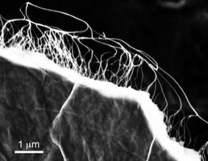
Here’s an image of graphene infused with carbon nantoubes used in the supercapacitor film,

A scanning electron microscope image shows freestanding graphene film with carbon nanotubes attached. The material is part of a project to create lightweight films containing super capacitors that charge quickly and store energy. Courtesy of Nunzio Motta/Queensland University of Technology - See more at: http://news.rice.edu/2014/11/07/supercharged-panels-may-power-cars/#sthash.0RPsIbMY.dpuf

A scanning electron microscope image shows freestanding graphene film with carbon nanotubes attached. The material is part of a project to create lightweight films containing super capacitors that charge quickly and store energy. Courtesy of Nunzio Motta/Queensland University of Technology

Here are links to and citations for the two papers published by the researchers,

Graphene-based supercapacitor with carbon nanotube film as highly efficient current collector by Marco Notarianni, Jinzhang Liu, Francesca Mirri, Matteo Pasquali, and Nunzio Motta. Nanotechnology Volume 25 Number 43 doi:10.1088/0957-4484/25/43/435405

High performance all-carbon thin film supercapacitors by Jinzhang Liu, Francesca Mirri, Marco Notarianni, Matteo Pasquali, and Nunzio Motta. Journal of Power Sources Volume 274, 15 January 2015, Pages 823–830 DOI: 10.1016/j.jpowsour.2014.10.104

Both articles are behind paywalls.

One final note, Dexter Johnson provides some insight into issues with graphene-based supercapacitors and what makes this proposed application attractive in his Nov. 7, 2014 post on the Nanoclast blog (on the IEEE [Institute of Electrical and Electronics Engineers] website; Note: Links have been removed),

The hope has been that someone could make graphene electrodes for supercapacitors that would boost their energy density into the range of chemical-based batteries. The supercapacitors currently on the market have on average an energy density around 28 Wh/kg, whereas a Li-ion battery holds about 200Wh/kg. That’s a big gap to fill.

The research in the field thus far has indicated that graphene’s achievable surface area in real devices—the factor that determines how many ions a supercapacitor electrode can store, and therefore its energy density—is not any better than traditional activated carbon. In fact, it may not be much better than a used cigarette butt.

Though graphene may not help increase supercapacitors’ energy density, its usefulness in this application may lie in the fact that its natural high conductivity will allow superconductors to operate at higher frequencies than those that are currently on the market. Another likely benefit that graphene will yield comes from the fact that it can be structured and scaled down, unlike other supercapacitor materials.

I recommend reading Dexter’s commentary in its entirety.

*’University of Queensland’ corrected to “Queensland University of Technology’ on Nov. 10, 2014 at 1335 PST.

* ‘super-capacitor’ changed to ‘supercapacitor’ on April 29, 2015.

NASA, super-black nanotechnology, and an International Space Station livestreamed event

A super-black nanotechnology-enabled coating (first mentioned here in a July 18, 2013 posting featuring work by John Hagopian, an optics engineer at the US National Aeronautics and Space Administration [NASA’s] Goddard Space Flight Center on this project) is about to be tested in outer space. From an Oct. 23, 2014 news item on Nanowerk,

An emerging super-black nanotechnology that is to be tested for the first time this fall on the International Space Station will be applied to a complex, 3-D component critical for suppressing stray light in a new, smaller, less-expensive solar coronagraph designed to ultimately fly on the orbiting outpost or as a hosted payload on a commercial satellite.

The super-black carbon-nanotube coating, whose development is six years in the making, is a thin, highly uniform coating of multi-walled nanotubes made of pure carbon about 10,000 times thinner than a strand of human hair. Recently delivered to the International Space Station for testing, the coating is considered especially promising as a technology to reduce stray light, which can overwhelm faint signals that sensitive detectors are supposed to retrieve.

An Oct. 24, 2014 NASA news release by Lori Keesey, which originated the news item, further describes the work being done on the ground simultaneous to the tests on the International Space Station,

While the coating undergoes testing to determine its robustness in space, a team at NASA’s Goddard Space Flight Center in Greenbelt, Maryland, will apply the carbon-nanotube coating to a complex, cylindrically shaped baffle — a component that helps reduce stray light in telescopes.

Goddard optical engineer Qian Gong designed the baffle for a compact solar coronagraph that Principal Investigator Nat Gopalswamy is now developing. The goal is [to] build a solar coronagraph that could deploy on the International Space Station or as a hosted payload on a commercial satellite — a much-needed capability that could guarantee the continuation of important space weather-related measurements.

The effort will help determine whether the carbon nanotubes are as effective as black paint, the current state-of-the-art technology, for absorbing stray light in complex space instruments and components.

Preventing errant light is an especially tricky challenge for Gopalswamy’s team. “We have to have the right optical system and the best baffles going,” said Doug Rabin, a Goddard heliophysicist who studies diffraction and stray light in coronagraphs.

The new compact coronagraph — designed to reduce the mass, volume, and cost of traditional coronagraphs by about 50 percent — will use a single set of lenses, rather than a conventional three-stage system, to image the solar corona, and more particularly, coronal mass ejections (CMEs). These powerful bursts of solar material erupt and hurdle across the solar system, sometimes colliding with Earth’s protective magnetosphere and posing significant hazards to spacecraft and astronauts.

“Compact coronagraphs make greater demands on controlling stray light and diffraction,” Rabin explained, adding that the corona is a million times fainter than the sun’s photosphere. Coating the baffle or occulter with the carbon-nanotube material should improve the component’s overall performance by preventing stray light from reaching the focal plane and contaminating measurements.

The project is well timed and much needed, Rabin added.

Currently, the heliophysics community receives coronagraphic measurements from the Solar and Heliospheric Observatory (SOHO) and the Solar Terrestrial Relations Observatory (STEREO).

“SOHO, which we launched in 1995, is one of our Great Observatories,” Rabin said. “But it won’t last forever.” Although somewhat newer, STEREO has operated in space since 2006. “If one of these systems fails, it will affect a lot of people inside and outside NASA, who study the sun and forecast space weather. Right now, we have no scheduled mission that will carry a solar coronagraph. We would like to get a compact coronagraph up there as soon as possible,” Rabin added.

Ground-based laboratory testing indicates it could be a good fit. Testing has proven that the coating absorbs 99.5 percent of the light in the ultraviolet and visible and 99.8 percent in the longer infrared bands due to the fact that the carbon atoms occupying the tiny nested tubes absorb the light and prevent it from reflecting off surfaces, said Goddard optics engineer John Hagopian, who is leading the technology’s advancement. Because only a tiny fraction of light reflects off the coating, the human eye and sensitive detectors see the material as black — in this case, extremely black.

“We’ve made great progress on the coating,” Hagopian said. “The fact the coatings have survived the trip to the space station already has raised the maturity of the technology to a level that qualifies them for flight use. In many ways the external exposure of the samples on the space station subjects them to a much harsher environment than components will ever see inside of an instrument.”

Given the need for a compact solar coronagraph, Hagopian said he’s especially excited about working with the instrument team. “This is an important instrument-development effort, and, of course, one that could showcase the effectiveness of our technology on 3-D parts,” he said, adding that the lion’s share of his work so far has concentrated on 2-D applications.

By teaming with Goddard technologist Vivek Dwivedi, Hagopian believes the baffle project now is within reach. Dwivedi is advancing a technique called atomic layer deposition (ALD) that lays down a catalyst layer necessary for carbon-nanotube growth on complex, 3-D parts. “Previous ALD chambers could only hold objects a few millimeters high, while the chamber Vivek has developed for us can accommodate objects 20 times bigger; a necessary step for baffles of this type,” Hagopian said.

Other NASA researchers have flown carbon nanotubes on the space station, but their samples were designed for structural applications, not stray-light suppression — a completely different use requiring that the material demonstrate greater absorption properties, Hagopian said.

“We have extreme stray light requirements. Let’s see how this turns out,” Rabin said.

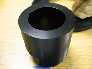
The researchers from NASA have kindly made available an image of a baffle prior to receiving its super-black coating,

This is a close-up view of a baffle that will be coated with a carbon-nanotube coating. Image Credit:  NASA Goddard/Paul Nikulla

This is a close-up view of a baffle that will be coated with a carbon-nanotube coating.
Image Credit: NASA Goddard/Paul Nikulla

There’s more information about the project in this August 12, 2014 NASA news release first announcing the upcoming test.

Serendipitously or not, NASA is hosting an interactive Space Technology Forum on Oct. 27, 2014 (this coming Monday) focusing on technologies being demonstrated on the International Space Station (ISS) according to an Oct. 20, 2014 NASA media advisory,

Media are invited to interact with NASA experts who will answer questions about technologies being demonstrated on the International Space Station (ISS) during “Destination Station: ISS Technology Forum” from 10 to 11 a.m. EDT (9 to 10 a.m. CDT [7 to 8 am PDT]) Monday, Oct. 27, at the U.S. Space & Rocket Center in Huntsville, Alabama.

The forum will be broadcast live on NASA Television and the agency’s website.

The Destination Station forums are a series of live, interactive panel discussions about the space station. This is the second in the series, and it will feature a discussion on how technologies are tested aboard the orbiting laboratory. Thousands of investigations have been performed on the space station, and although they provide benefits to people on Earth, they also prepare NASA to send humans farther into the solar system than ever before.

Forum panelists and exhibits will focus on space station environmental and life support systems; 3-D printing; Space Communications and Navigation (SCaN) systems; and Synchronized Position Hold, Engage, Reorient, Experimental Satellites (SPHERES).

The forum’s panelists are:
– Jeffrey Sheehy, senior technologist in NASA’s Space Technology Mission Directorate
– Robyn Gatens, manager for space station System and Technology Demonstration, and Environmental Control Life Support System expert
– Jose Benavides, SPHERES chief engineer
– Rich Reinhart, principal investigator for the SCaN Testbed
– Niki Werkeiser, project manager for the space station 3-D printer

During the forum, questions will be taken from the audience, including media, students and social media participants. Online followers may submit questions via social media using the hashtag, #asknasa. [emphasis mine] …

The “Destination Station: ISS Technology Forum” coincides with the 7th Annual Von Braun Memorial Symposium at the University of Alabama in Huntsville Oct. 27-29. Media can attend the three-day symposium, which features NASA officials, including NASA Administrator Charles Bolden, Associate Administrator for Human Exploration and Operation William Gerstenmaier and Assistant Deputy Associate Administrator for Exploration Systems Development Bill Hill. Jean-Jacques Dordain, director general of the European Space Agency, will be a special guest speaker. Representatives from industry and academia also will be participating.

For NASA TV streaming video, scheduling and downlink information, visit:

http://www.nasa.gov/nasatv

For more information on the International Space Station and its crews, visit:

http://www.nasa.gov/station

I have checked out the livestreaming/tv site and it appears that registration is not required for access. Sadly, I don’t see any the ‘super-black’ coating team members mentioned in the news release on the list of forum participants.

ETA Oct. 27, 2014: You can check out Dexter Johnson’s Oct. 24, 2014 posting on the Nanoclast blog (on the IEEE [Institute of Electrical and Electronics Engineers] website for a little more information

Next supercapacitor: crumpled graphene?

An Oct. 3, 2014 news item on ScienceDaily features the use of graphene as a possible supercapacitor,

When someone crumples a sheet of paper, that usually means it’s about to be thrown away. But researchers have now found that crumpling a piece of graphene “paper” — a material formed by bonding together layers of the two-dimensional form of carbon — can actually yield new properties that could be useful for creating extremely stretchable supercapacitors to store energy for flexible electronic devices.

The finding is reported in the journal Scientific Reports by MIT’s {Massachusetts Institute of Technology] Xuanhe Zhao, an assistant professor of mechanical engineering and civil and environmental engineering, and four other authors. The new, flexible superconductors should be easy and inexpensive to fabricate, the team says.

An Oct. 3, 2014 MIT news release by David Chandler (also on EurekAlert), which originated the news item, explains the technology at more length,

“Many people are exploring graphene paper: It’s a good candidate for making supercapacitors, because of its large surface area per mass,” Zhao says. Now, he says, the development of flexible electronic devices, such as wearable or implantable biomedical sensors or monitoring devices, will require flexible power-storage systems.

Like batteries, supercapacitors can store electrical energy, but they primarily do so electrostatically, rather than chemically — meaning they can deliver their energy faster than batteries can. Now Zhao and his team have demonstrated that by crumpling a sheet of graphene paper into a chaotic mass of folds, they can make a supercapacitor that can easily be bent, folded, or stretched to as much as 800 percent of its original size. The team has made a simple supercapacitor using this method as a proof of principle.

The material can be crumpled and flattened up to 1,000 times, the team has demonstrated, without a significant loss of performance. “The graphene paper is pretty robust,” Zhao says, “and we can achieve very large deformations over multiple cycles.” Graphene, a structure of pure carbon just one atom thick with its carbon atoms arranged in a hexagonal array, is one of the strongest materials known.

To make the crumpled graphene paper, a sheet of the material was placed in a mechanical device that first compressed it in one direction, creating a series of parallel folds or pleats, and then in the other direction, leading to a chaotic, rumpled surface. When stretched, the material’s folds simply smooth themselves out.

Forming a capacitor requires two conductive layers — in this case, two sheets of crumpled graphene paper — with an insulating layer in between, which in this demonstration was made from a hydrogel material. Like the crumpled graphene, the hydrogel is highly deformable and stretchable, so the three layers remain in contact even while being flexed and pulled.

Though this initial demonstration was specifically to make a supercapacitor, the same crumpling technique could be applied to other uses, Zhao says. For example, the crumpled graphene material might be used as one electrode in a flexible battery, or could be used to make a stretchable sensor for specific chemical or biological molecules.

Here is a link to and a citation for the paper,

Stretchable and High-Performance Supercapacitors with Crumpled Graphene Papers by Jianfeng Zang, Changyong Cao, Yaying Feng, Jie Liu, & Xuanhe Zhao. Scientific Reports 4, Article number: 6492 doi:10.1038/srep06492 Published 01 October 2014

This is an open access article.

ETA Oct. 8, 2014: Dexter Johnson of the Nanoclast blog on the IEEE (Institute of Electrical and Electronics Engineers) website has an Oct. 7, 2014 post where he comments about the ‘flexibility’ aspect of this work.

Researchers at Purdue University (Indiana, US) and at the Indian Institute of Technology Madras (Chennai, India) develop Star Trek-type ‘tricorders’

To be clear, the Star Trek-type ‘tricorder’ referred to in the heading is, in fact, a hand-held spectrometer and the research from Purdue University and the Indian Institute of Technology Madras represents a developmental leap forward, not a new product. From a March 26, 2014 news item on Azonano,

Nanotechnology is advancing tools likened to Star Trek’s “tricorder” that perform on-the-spot chemical analysis for a range of applications including medical testing, explosives detection and food safety.

Researchers found that when paper used to collect a sample was coated with carbon nanotubes, the voltage required was 1,000 times reduced, the signal was sharpened and the equipment was able to capture far more delicate molecules.

Dexter Johnson in his March 26, 2014 posting (Nanoclast blog on the IEEE [Institute of Electrical and Electronics Engineers] website) provides some background information about the race to miniaturize spectrometers (Note: A link has been removed),

Recent research has been relying on nanomaterials to build smaller spectrometers. Late last year, a group at the Technische Universität Dresden and the Fraunhofer Institute in Germany developed a novel, miniature spectrometer, based on metallic nanowires, that was small enough to fit into a mobile phone.

Dexter goes on to provide a summary about this latest research, which I strongly recommend reading, especially if you don’t have the patience to read the rest of the news release. The March 25, 2014 Purdue University news release by Elizabeth K. Gardner, which originated the news item, provides insight from the researchers,

“This is a big step in our efforts to create miniature, handheld mass spectrometers for the field,” said R. Graham Cooks, Purdue’s Henry B. Hass Distinguished Professor of Chemistry. “The dramatic decrease in power required means a reduction in battery size and cost to perform the experiments. The entire system is becoming lighter and cheaper, which brings it that much closer to being viable for easy, widespread use.”

Cooks and Thalappil Pradeep, a professor of chemistry at the Indian Institute of Technology Madras, Chennai, led the research.

“Taking science to the people is what is most important,” Pradeep said. “Mass spectrometry is a fantastic tool, but it is not yet on every physician’s table or in the pocket of agricultural inspectors and security guards. Great techniques have been developed, but we need to hone them into tools that are affordable, can be efficiently manufactured and easily used.”

The news release goes on to describe the research,

The National Science Foundation-funded study used an analysis technique developed by Cooks and his colleagues called PaperSpray™ ionization. The technique relies on a sample obtained by wiping an object or placing a drop of liquid on paper wet with a solvent to capture residues from the object’s surface. A small triangle is then cut from the paper and placed on a special attachment of the mass spectrometer where voltage is applied. The voltage creates an electric field that turns the mixture of solvent and residues into fine droplets containing ionized molecules that pop off and are vacuumed into the mass spectrometer for analysis. The mass spectrometer then identifies the sample’s ionized molecules by their mass.

The technique depends on a strong electric field and the nanotubes act like tiny antennas that create a strong electric field from a very small voltage. One volt over a few nanometers creates an electric field equivalent to 10 million volts over a centimeter, Pradeep said.

“The trick was to isolate these tiny, nanoscale antennae and keep them from bundling together because individual nanotubes must project out of the paper,” he said. “The carbon nanotubes work well and can be dispersed in water and applied on suitable substrates.”

The Nano Mission of the Government of India supported the research at the Indian Institute of Technology Madras and graduate students Rahul Narayanan and Depanjan Sarkar performed the experiments.

In addition to reducing the size of the battery required and energy cost to run the tests, the new technique also simplified the analysis by nearly eliminating background noise, Cooks said.

“Under these conditions, the analysis is nearly noise free and a sharp, clear signal of the sample is delivered,” he said. “We don’t know why this is – why background molecules that surround us in the air or from within the equipment aren’t being ionized and entering into the analysis. It’s a puzzling, but pleasant surprise.”

The reduced voltage required also makes the method gentler than the standard PaperSpray™ ionization techniques.

“It is a very soft method,” Cooks said. “Fragile molecules and complexes are able to hold together here when they otherwise wouldn’t. This could lead to other potential applications.”

The team plans to investigate the mechanisms behind the reduction in background noise and potential applications of the gentle method, but the most promising aspect of the new technique is its potential to miniaturize the mass spectrometry system, Cooks said.

Here’s a link to and a citation for the paper,

Molecular Ionization from Carbon Nanotube Paper by Rahul Narayanan, Depanjan Sarkar, Prof. R. Graham Cooks, and Prof. Thalappil Pradeep. Angewandte Chemie International Edition Article first published online: 18 MAR 2014 DOI: 10.1002/anie.201311053

© 2014 WILEY-VCH Verlag GmbH & Co. KGaA, Weinheim

This paper is behind a paywall.

Injectable and more powerful* batteries for live salmon

Today’s live salmon may sport a battery for monitoring purposes and now scientists have developed one that is significantly more powerful according to a Feb. 17, 2014 Pacific Northwest National Laboratory (PNNL) news release (dated Feb. 18, 2014 on EurekAlert),

Scientists have created a microbattery that packs twice the energy compared to current microbatteries used to monitor the movements of salmon through rivers in the Pacific Northwest and around the world.

The battery, a cylinder just slightly larger than a long grain of rice, is certainly not the world’s smallest battery, as engineers have created batteries far tinier than the width of a human hair. But those smaller batteries don’t hold enough energy to power acoustic fish tags. The new battery is small enough to be injected into an organism and holds much more energy than similar-sized batteries.

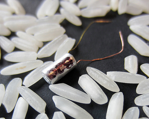
Here’s a photo of the battery as it rests amongst grains of rice,

The microbattery created by Jie Xiao and Daniel Deng and colleagues, amid grains of rice. Courtesy PNNL

The microbattery created by Jie Xiao and Daniel Deng and colleagues, amid grains of rice. Courtesy PNNL

The news release goes on to explain why scientists are developing a lighter battery for salmon and how they achieved their goal,

For scientists tracking the movements of salmon, the lighter battery translates to a smaller transmitter which can be inserted into younger, smaller fish. That would allow scientists to track their welfare earlier in the life cycle, oftentimes in the small streams that are crucial to their beginnings. The new battery also can power signals over longer distances, allowing researchers to track fish further from shore or from dams, or deeper in the water.

“The invention of this battery essentially revolutionizes the biotelemetry world and opens up the study of earlier life stages of salmon in ways that have not been possible before,” said M. Brad Eppard, a fisheries biologist with the Portland District of the U.S. Army Corps of Engineers.

“For years the chief limiting factor to creating a smaller transmitter has been the battery size. That hurdle has now been overcome,” added Eppard, who manages the Portland District’s fisheries research program.

The Corps and other agencies use the information from tags to chart the welfare of endangered fish and to help determine the optimal manner to operate dams. Three years ago the Corps turned to Z. Daniel Deng, a PNNL engineer, to create a smaller transmitter, one small enough to be injected, instead of surgically implanted, into fish. Injection is much less invasive and stressful for the fish, and it’s a faster and less costly process.

“This was a major challenge which really consumed us these last three years,” said Deng. “There’s nothing like this available commercially, that can be injected. Either the batteries are too big, or they don’t last long enough to be useful. That’s why we had to design our own.”

Deng turned to materials science expert Jie Xiao to create the new battery design.

To pack more energy into a small area, Xiao’s team improved upon the “jellyroll” technique commonly used to make larger household cylindrical batteries. Xiao’s team laid down layers of the battery materials one on top of the other in a process known as lamination, then rolled them up together, similar to how a jellyroll is created. The layers include a separating material sandwiched by a cathode made of carbon fluoride and an anode made of lithium.

The technique allowed her team to increase the area of the electrodes without increasing their thickness or the overall size of the battery. The increased area addresses one of the chief problems when making such a small battery — keeping the impedance, which is a lot like resistance, from getting too high. High impedance occurs when so many electrons are packed into a small place that they don’t flow easily or quickly along the routes required in a battery, instead getting in each other’s way. The smaller the battery, the bigger the problem.

Using the jellyroll technique allowed Xiao’s team to create a larger area for the electrons to interact, reducing impedance so much that the capacity of the material is about double that of traditional microbatteries used in acoustic fish tags.

“It’s a bit like flattening wads of Play-Doh, one layer at a time, and then rolling them up together, like a jelly roll,” says Xiao. “This allows you to pack more of your active materials into a small space without increasing the resistance.”

The new battery is a little more than half the weight of batteries currently used in acoustic fish tags — just 70 milligrams, compared to about 135 milligrams — and measures six millimeters long by three millimeters wide. The battery has an energy density of about 240 watt hours per kilogram, compared to around 100 for commercially available silver oxide button microbatteries.

The battery holds enough energy to send out an acoustic signal strong enough to be useful for fish-tracking studies even in noisy environments such as near large dams. The battery can power a 744-microsecond signal sent every three seconds for about three weeks, or about every five seconds for a month. It’s the smallest battery the researchers know of with enough energy capacity to maintain that level of signaling.

The batteries also work better in cold water where salmon often live, sending clearer signals at low temperatures compared to current batteries. That’s because their active ingredients are lithium and carbon fluoride, a chemistry that is promising for other applications but has not been common for microbatteries.

Last summer in Xiao’s laboratory, scientists Samuel Cartmell and Terence Lozano made by hand more than 1,000 of the rice-sized batteries. It’s a painstaking process, cutting and forming tiny snippets of sophisticated materials, putting them through a flattening device that resembles a pasta maker, binding them together, and rolling them by hand into tiny capsules. Their skilled hands rival those of surgeons, working not with tissue but with sensitive electronic materials.

A PNNL team led by Deng surgically implanted 700 of the tags into salmon in a field trial in the Snake River last summer. Preliminary results show that the tags performed extremely well. The results of that study and more details about the smaller, enhanced fish tags equipped with the new microbattery will come out in a forthcoming publication. Battelle, which operates PNNL, has applied for a patent on the technology.

I notice that while the second paragraph of the news release (in the first excerpt) says the battery is injectable, the final paragraph (in the second excerpt) says the team “surgically implanted” the tags with their new batteries into the salmon.

Here’s a link to and a citation for the newly published article in Scientific Reports,

Micro-battery Development for Juvenile Salmon Acoustic Telemetry System Applications by Honghao Chen, Samuel Cartmell, Qiang Wang, Terence Lozano, Z. Daniel Deng, Huidong Li, Xilin Chen, Yong Yuan, Mark E. Gross, Thomas J. Carlson, & Jie Xiao. Scientific Reports 4, Article number: 3790 doi:10.1038/srep03790 Published 21 January 2014

This paper is open access.

* I changed the headline from ‘Injectable batteries for live salmon made more powerful’ to ‘Injectable and more powerful batteries for live salmon’  to better reflect the information in the news release. Feb. 19, 2014 at 11:43 am PST.

ETA Feb. 20, 2014: Dexter Johnson has weighed in on this very engaging and practical piece of research in a Feb. 19, 2014 posting on his Nanoclast blog (on the IEEE [Institute of Electrical and Electronics Engineers]) website (Note: Links have been removed),

There’s no denying that building the world’s smallest battery is a notable achievement. But while they may lay the groundwork for future battery technologies, today such microbatteries are mostly laboratory curiosities.

Developing a battery that’s no bigger than a grain of rice—and that’s actually useful in the real world—is quite another kind of achievement. Researchers at Pacific Northwest National Laboratory (PNNL) have done just that, creating a battery based on graphene that has successfully been used in monitoring the movements of salmon through rivers.

The microbattery is being heralded as a breakthrough in biotelemetry and should give researchers never before insights into the movements and the early stages of life of the fish.

The battery is partly made from a fluorinated graphene that was described last year …

Institute of Electrical and Electronics Engineers (IEEE) 2014 international nanotechnology conference in Toronto, Canada

August 18 – 21, 2014 are the dates for the IEEE (Institute for Electrical and Electronics Engineers) 14th International Conference on Nanotechnology.  The deadline for submitting abstracts is March 15, 2014. Here’s a bit more about the conference, from the homepage,

IEEE Nano is one of the largest Nanotechnology conferences in the world, bringing together the brightest engineers and scientists through collaboration and the exchange of ideas.

IEEE Nano 2014 will provide researchers and others in the Nanotechnology field the ability to interact and advance their work through various speakers and workshop sessions.

Possible Topics for Papers

Environmental Health and Safety of Nanotechnology
Micro-to-nano-scale bridging
Modeling and Simulation
Nanobiology:
•Nanobiomedicine
•Nanobiosystems
•Applications of Biopolymer Nanoparticles for Drug Delivery
Nanoelectronics:
•Non-Carbon Based
•Carbon Based
•Circuits and Architecture
Nanofabrication and Nanoassemblies
Nanofluidics:
•Modeling and Theory
•Applications
Nanomagnetics
Nanomanufacturing
Nanomaterials:
•2-D Materials beyond Graphene
•Synthesis and Characterization
•Applications and Enabled Systems
Nanometrology and Nanocharacterization
Nanopackaging
Nano-optics, Nano-optoelectronics and Nano-photonics:
•Novel fabrication and integration approaches
•Optical Nano-devices
Nanorobotics and Nanomanipulation
Nanoscale Communication and Networks
Nanosensors and Actuators
Nanotechnology Enabled Energy
NEMS
NEMS/Applications

There is a conference Call For Papers webpage where you can get more information.

Invited speakers include,

John Polanyi
Professor
University of Toronto, Canada

John Polanyi, educated at Manchester University, England, was a postdoctoral fellow at Princeton University and at the National Research Council of Canada. He is a faculty member in the Department of Chemistry at the University of Toronto, a member of the Queen’s Privy Council for Canada (P.C.), and a Companion of the Order of Canada (C.C.). His awards include the 1986 Nobel Prize in Chemistry. He has written extensively on science policy, the control of armaments, peacekeeping and human rights.

Charles Lieber
Professor Charles M. Lieber
Mark Hyman Professor of Chemistry
Department of Chemistry and Chemical Biology
Harvard University

Charles M. Lieber is regarded as a leading chemist worldwide and recognized as a pioneer in the nanoscience and nanotechnology fields. He completed his doctoral studies at Stanford University and currently holds a joint appointment in the Department of Chemistry and Chemical Biology at Harvard University, as the Mark Hyman Professor of Chemistry, and the School of Engineering and Applied Sciences. Lieber is widely known for his contributions to the synthesis, understanding and assembly of nanoscale materials, as well as the founding of two nanotechnology companies: Nanosys and Vista Therapeutics.

Lieber’s achievements have been recognized by a large number of awards, including the Feynman Prize for Nanotechnology (2002), World Technology award in Materials (2003 and 2004) and the Wolf Prize in Chemistry (2012). He has published more than 350 papers in peer-reviewed journals and is the primary inventor on over 35 patents.

Arthur Carty
Professor & Executive Director [Waterloo Institute for Nanotechnology]
University of Waterloo, Canada

Arthur Carty has a PhD in inorganic chemistry from the University of Nottingham in the UK. He is currently the Executive Director of the Waterloo Institute for Nanotechnology and research professor in the Department of Chemistry at the University of Waterloo.

Previously, Dr. Carty served in Canada as the National Science Advisor to the Prime Minister and President of the National Research Council (Canada). He was awarded the Order of Canada and holds 14 honorary doctorates.

His research interests are focused on organometallic chemistry and new materials. [Dr. Carty is chair of The Expert Panel on the State of Canada’s Science Culture; an assessment being conducted by the Canadian Council of Academies as per my Feb. 22, 2013 posting and Dr. Carty is giving a Keynote lecture titled: ‘Small World, Large Impact: Driving a Materials Revolution Through Nanotechnology’ at the 2014 TAPPI (Technical Association for the Pulp, Paper, Packaging and Converting Industries) nanotechnology conference, June 23-26, 2014 in Vancouver, Canada as per my Nov. 14, 2013 posting.]

William Milne
Professor
University of Cambridge, UK

Bill Milne FREng,FIET,FIMMM has been Head of Electrical Engineering at Cambridge University since 1999 and Director of the Centre for Advanced Photonics and Electronics (CAPE) since 2005. In 1996 he was appointed to the ‘‘1944 Chair in Electrical Engineering’’. He obtained his BSc from St Andrews University in Scotland in 1970 and then went on to read for a PhD in Electronic Materials at Imperial College London. He was awarded his PhD and DIC in 1973 and, in 2003, a D.Eng (Honoris Causa) from University of Waterloo, Canada. He was elected a Fellow of The Royal Academy of Engineering in 2006. He was awarded the J.J. Thomson medal from the IET in 2008 and the NANOSMAT prize in 2010 for excellence in nanotechnology. His research interests include large area Si and carbon based electronics, graphene, carbon nanotubes and thin film materials. Most recently he has been investigating MEMS, SAW and FBAR devices and SOI based micro heaters for ( bio) sensing applications. He has published/presented ~ 800 papers in these areas, of which ~ 150 were invited. He co-founded Cambridge Nanoinstruments with 3 colleagues from the Department and this was bought out by Aixtron in 2008 and in 2009 co-founded Cambridge CMOS Sensors with Julian Gardner from Warwick Univ. and Florin Udrea from Cambridge Univ.

Shuit-Tong Lee
Institute of Functional Nano & Soft Materials (FUNSOM)
Collaboration Innovation Center of Suzhou Nano Science and Technology
College of Nano Science and Technology (CNST)
Soochow University, China
Email: apannale@suda.edu.c

Prof. Lee is the member (academician) of Chinese Academy of Sciences and the fellow of TWAS (the academy of sciences for the developing world). He is a distinguished scientist in material science and engineering. Prof. Lee is the Founding Director of Functional Nano & Soft Materials Laboratory (FUNSOM) and Director of the College of Chemistry, Chemical Engineering and Materials Science at Soochow University. He is also a Chair Professor of Materials Science and Founding Director of the Center of Super-Diamond and Advanced Films (COSDAF) at City University of Hong Kong and the Founding Director of Nano-Organic Photoelectronic Laboratory at the Technical Institute of Physics and Chemistry, CAS. He was the Senior Research Scientist and Project Manager at the Research Laboratories of Eastman Kodak Company in the US before he joined City University of Hong Kong in 1994. He won the Humboldt Senior Research Award (Germany) in 2001 and a Croucher Senior Research Fellowship from the Croucher Foundation (HK) in 2002 for the studies of “Nucleation and growth of diamond and new carbon based materials” and “Oxide assisted growth and applications of semiconducting nanowires”, respectively. He also won the National Natural Science Award of PRC (second class) in 2003 and 2005 for the above research achievements. Recently, he was awarded the 2008 Prize for Scientific and Technological Progress of Ho Leung Ho Lee Foundation. Prof. Lee’s research work has resulted in more than 650 peer-reviewed publications in prestigious chemistry, physics and materials science journals, 6 book chapters and over 20 US patents, among them 5 papers were published in Science and Nature (London) and some others were selected as cover papers. His papers have more than 10,000 citations by others, which is ranked within world top 25 in the materials science field according to ESI and ISI citation database.

Sergej Fatikow
Full Professor, Dr.-Ing. habil.
Head, Division for Microrobotics & Control Engineering (AMiR)
University of Oldenburg, Germany

Professor Sergej Fatikow studied electrical engineering and computer science at the Ufa Aviation Technical University in Russia, where he received his doctoral degree in 1988 with work on fuzzy control of complex non-linear systems. After that he worked until 1990 as a lecturer at the same university. During his work in Russia he published over 30 papers and successfully applied for over 50 patents in intelligent control and mechatronics. In 1990 he moved to the Institute for Process Control and Robotics at the University of Karlsruhe in Germany, where he worked as a postdoctoral scientific researcher and since 1994 as Head of the research group “Microrobotics and Micromechatronics”. He became an assistant professor in 1996 and qualified for a full faculty position by habilitation at the University of Karlsruhe in 1999. In 2000 he accepted a faculty position at the University of Kassel, Germany. A year later, he was invited to establish a new Division for Microrobotics and Control Engineering (AMiR) at the University of Oldenburg, Germany. Since 2001 he is a full professor in the Department of Computing Science and Head of AMiR. His research interests include micro- and nanorobotics, automated robot-based nanohandling in SEM, AFM-based nanohandling, sensor feedback at nanoscale, and neuro-fuzzy robot control. He is author of three books on microsystem technology, microrobotics and microassembly, robot-based nanohandling, and automation at nanoscale, published by Springer in 1997, Teubner in 2000, and Springer in 2008. Since 1990 he published over 100 book chapters and journal papers and over 200 conference papers. Prof. Fatikow is Founding Chair of the International Conference on Manipulation, Manufacturing and Measurement on the Nanoscale (3M-NANO) and Europe- Chair of IEEE-RAS Technical Committee on Micro/Nano Robotics and Automation.

Seiji Samukawa
Distinguished Professor
Innovative Energy Research Center, Institute of Fluid Science, Tohoku University
World Premier International Center Initiative, Advanced Institute for Materials Research, Tohoku University, Sendai, Japan

Dr. Seiji Samukawa received a BSc in 1981 from the Faculty of Technology of Keio University and joined NEC Corporation the same year. At NEC Microelectronics Research Laboratories, he was the lead researcher of a group performing fundamental research on advanced plasma etching processes for technology under 0.1 μm. While there, he received the Ishiguro Award—given by NEC’s R&D Group and Semiconductor Business Group— for his work in applying a damage-free plasma etching process to a mass-production line. After spending several years in the business world, however, he returned to Keio University, obtaining a PhD in engineering in 1992. Since 2000, he has served as professor at the Institute of Fluid Science at Tohoku University and developed ultra-low-damage microfabrication techniques that tap into the essential nature of nanomaterials and developed innovative nanodevices. He is also carrying out pioneering, creative research on bio-template technologies, which are based on a completely new concept of treating the super-molecules of living organisms. His motto when conducting research is to “always aim toward eventual practical realization.”

In recognition of his excellent achievements outlined above, he has been elected as a Distinguished Professor of Tohoku University and has been a Fellow of the Japan Society of Applied Physics since 2008 and a Fellow of the American Vacuum Society since 2009. His significant scientific achievements earned him the Outstanding Paper Award at the International Conference on Micro and Nanotechnology (1997), Best Review Paper Award (2001), Japanese Journal of Applied Physics (JJAP) Editorial Contribution Award (2003), Plasma Electronics Award (2004), Fellow Award (2008), JJAP Paper Award (2008) from the Japan Society of Applied Physics, Distinguished Graduate Award (2005) from Keio University, Ichimura Award (2008) from the New Technology Development Foundation, Commendation for Science and Technology from the Minister of Education, Culture, Sports, Science and Technology (2009), Fellow Award of American Vacuum Society (2009), Plasma Electronics Award from the Japan Society of Applied Physics (2010), Best Paper Award from the Japan Society of Applied Physics (2010), and Plasma Prize from the Plasma Science and Technology Division of American Vacuum Society (2010).

Haixia (Alice) Zhang
Professor
Institute of Microelectronics
Peking University, China

Haixia(Alice) Zhang, Professor, Institute of Microelectronics, Peking Universituy. She was served on the general chair of IEEE NEMS 2013 Conference, the organizing chair of Transducers’11. As the founder of the International Contest of Applications in Network of things (iCAN), she organized this world-wide event since 2007. She was elected the director of Integrated Micro/Nano System Engineering Center in 2006, the deputy secretary-general of Chinese Society of Micro-Nano Technology in 2005, the Co-chair of Chinese International NEMS Network (CINN) and serves as the chair of IEEE NTC Beijing Chapter. At 2006, Dr. Zhang won National Invention Award of Science & Technology. Her research fields include MEMS Design and Fabrication Technology, SiC MEMS and Micro Energy Technology.

Alice’s Wonderlab: http://www.ime.pku.edu.cn/alice

I wonder if the organizers will be including an Open Forum as they did at the 13th IEEE nanotechnology conference in China. It sounds a little more dynamic and fun than any of the sessions currently listed for the Toronto conference but these things are sometimes best organized in a relatively spontaneous fashion rather than as one of the more formal conference events (from the 13th conference Open Forum),

This Open Forum will be run like a Rump Session to have a lively discussion of various topics of interest to the IEEE Nanotechnology Community. The key to the success of this Forum is participation from the audience with their own opinions and comments on any Nanotechnology subject or issue they can think of. We expect the session to be lively, interesting, controversial, opinionated and more. Here are some topics or issues to think about:

  1. When are we ever going to have a large scale impact of nanotechnology ? Shouldn’t we be afraid that the stakeholders (Tax payers, Politicians) are going to run out of patience ?
  2. Is there a killer app or apps on the horizon ?
  3. Is there a future for carbon nanotubes in electronics ? It has been 15 years + now….
  4. Is there a future for graphene in electronics ?
  5. Is there a future for graphene in anything ? Or will it just run its course on every application people did previously for carbon nanotubes ?
  6. As engineers, are we doing anything different from the physicists/chemists ? Looks like we are also chasing the same old : trying to publish in Nature, Science, and other similar journals with huge impact factor ? Are we prepared adequately to play in someone else’s game ? Should we even be doing it ?
  7. As engineers, aren’t we supposed to come up with working widgets closer to manufacturing ?
  8. As engineers, are we going to take responsibility for the commercial future of nanotechnology as has been done in all previous success stories ?

This list is by no means exhaustive. Please come up with your own questions/issues and speak up at the session.

Good luck with your abstract.

3D printing and the environment (a panel discussion at the Woodrow Wilson International Center for Scholars), and new developments with metal 3D printing

I have combined two 3D printing items here. The first is an announcement from the Woodrow Wilson International Center for Scholars about an upcoming panel discussion (from the Nov. 25, 2013 announcement),

The Environmental Impacts of 3D Printing

3D printing allows for cheaper and quicker production of complex and novel items. The technology has been used by industry to build prototypes and specialized parts since the 1980s, but interest in desktop applications of the technology has increased in recent years as prices for the machines have dropped.

Proponents of the technology often cite the environmental benefits of 3D printing, though fundamental questions remain: What technologies are involved in 3D printing? How efficient are these technologies in the use of materials and energy? Does the design of printed objects reduce end-of-life options? Does more localized production reduce the carbon footprint? Will simplicity and ubiquity cause us to overprint things, just as we do with paper?

Robert Olson explored some of these questions in his article “3D Printing: A Boon or a Bane?” in the November/December 2013 issue of the Environmental Forum. The article discusses the enormous potential of 3D printing and examines the paucity of research on the environmental impacts of the technology.

Join us at the Wilson Center on Dec. 13 for an event looking at the growth of additive manufacturing and the potential environmental implications of the technology.

When: Dec. 13, 2013 from 9 a.m. – 11 a.m. EST

Who:

  • Robert Olson, Senior Fellow, Institute for Alternative Futures
  • David Rejeski, Director, Science and Technology Innovation Program, Wilson Center
  • John Pendergrass, Senior Attorney & Director of the State Center, Environmental Law Institute

There is more information on the Event page.

While this panel discussion is likely to be focused on polymer 3D printing, there are other developments in the 3D printing world as per a Nov. 26, 2013 Michigan Technological University (MTU) news release (also on EurekAlert, Dec. 2, 2013),

OK, so maybe you aren’t interested in making your own toys, cellphone cases, or glow-in-the-dark Christmas decorations. How about a brake drum?

Until now, 3D printing has been a polymer affair, with most people in the maker community using the machines to make all manner of plastic consumer goods, from tent stakes to chess sets. A new low-cost 3D printer developed by Michigan Technological University’s Joshua Pearce and his team could add hammers to that list. The detailed plans, software and firmware are all freely available and open-source, meaning anyone can use them to make their own metal 3D printer.

This open access technology is being made accessible to the maker community, preferably to the highly skilled and experienced members, (from the news release),

Pearce is the first to admit that his new printer is a work in progress. So far, the products he and his team have produced are no more intricate than a sprocket. But that’s because the technology is so raw. “Similar to the incredible churn in innovation witnessed with open-sourcing of the first RepRap plastic 3D printers, I anticipate rapid progress when the maker community gets their hands on it,” says Pearce, an associate professor of materials science and engineering/electrical and computer engineering. “Within a month, somebody will make one that’s better than ours, I guarantee it.”

Using under $1,500 worth of materials, including a small commercial MIG welder and an open-source microcontroller, Pearce’s team built a 3D metal printer than can lay down thin layers of steel to form complex geometric objects. Commercial metal printers are available, but they cost over half a million dollars.

His make-it-yourself metal printer is less expensive than off-the-shelf commercial plastic 3D printers and is affordable enough for home use, he said. However, because of safety concerns, Pearce suggests that for now it would be better off in the hands of a shop, garage or skilled DIYer, since it requires more safety gear and fire protection equipment than the typical plastic 3D printer.

While metal 3D printing opens new vistas, it also raises anew the specter of homemade firearms. Some people have already made guns with both commercial metal and plastic 3D printers, with mixed results. While Pearce admits to some sleepless nights as they developed the metal printer, he also believes that the good to come from all types of distributed manufacturing with 3D printing will far outweigh the dangers.

In previous work, his group has already shown that making products at home with a 3D printer is cheaper for the average American and that printing goods at home is greener than buying commercial goods.

In particular, expanded 3D printing would benefit people in the developing world, who have limited access to manufactured goods, and researchers, who can radically cut costs of scientific equipment to further their science, Pearce said. “Small and medium-sized enterprises would be able to build parts and equipment quickly and easily using downloadable, free and open-source designs, which could revolutionize the economy for the benefit of the many.”

“I really don’t know if we are mature enough to handle it,” he added cautiously, “but I think that with open-source approach, we are within reach of a Star Trek-like, post-scarcity society, in which ‘replicators’ can create a vast array of objects on demand, resulting in wealth for everyone at very little cost. Pretty soon, we’ll be able to make almost anything.”

There is a paper and here’s a citation,of sorts,

“A Low-Cost, Open-Source Metal 3-D Printer,” to be published Nov. 25 in IEEE Access (DOI: 10.1109/ACCESS.2013.2293018)

Unfortunately I’ve not been able to locate this paper on IEEE {Institute of Electrical and Electronics Engineers]  Access.