Tag Archives: Tohoku University

Graphene goes to the moon

The people behind the European Union’s Graphene Flagship programme (if you need a brief explanation, keep scrolling down to the “What is the Graphene Flagship?” subhead) and the United Arab Emirates have got to be very excited about the announcement made in a November 29, 2022 news item on Nanowerk, Note: Canadians too have reason to be excited as of April 3, 2023 when it was announced that Canadian astronaut Jeremy Hansen was selected to be part of the team on NASA’s [US National Aeronautics and Space Administration] Artemis II to orbit the moon (April 3, 2023 CBC news online article by Nicole Mortillaro) ·

Graphene Flagship Partners University of Cambridge (UK) and Université Libre de Bruxelles (ULB, Belgium) paired up with the Mohammed bin Rashid Space Centre (MBRSC, United Arab Emirates), and the European Space Agency (ESA) to test graphene on the Moon. This joint effort sees the involvement of many international partners, such as Airbus Defense and Space, Khalifa University, Massachusetts Institute of Technology, Technische Universität Dortmund, University of Oslo, and Tohoku University.

The Rashid rover is planned to be launched on 30 November 2022 [Note: the launch appears to have occurred on December 11, 2022; keep scrolling for more about that] from Cape Canaveral in Florida and will land on a geologically rich and, as yet, only remotely explored area on the Moon’s nearside – the side that always faces the Earth. During one lunar day, equivalent to approximately 14 days on Earth, Rashid will move on the lunar surface investigating interesting geological features.

A November 29, 2022 Graphene Flagship press release (also on EurekAlert), which originated the news item, provides more details,

The Rashid rover wheels will be used for repeated exposure of different materials to the lunar surface. As part of this Material Adhesion and abrasion Detection experiment, graphene-based composites on the rover wheels will be used to understand if they can protect spacecraft against the harsh conditions on the Moon, and especially against regolith (also known as ‘lunar dust’).

Regolith is made of extremely sharp, tiny and sticky grains and, since the Apollo missions, it has been one of the biggest challenges lunar missions have had to overcome. Regolith is responsible for mechanical and electrostatic damage to equipment, and is therefore also hazardous for astronauts. It clogs spacesuits’ joints, obscures visors, erodes spacesuits and protective layers, and is a potential health hazard.  

University of Cambridge researchers from the Cambridge Graphene Centre produced graphene/polyether ether ketone (PEEK) composites. The interaction of these composites with the Moon regolith (soil) will be investigated. The samples will be monitored via an optical camera, which will record footage throughout the mission. ULB researchers will gather information during the mission and suggest adjustments to the path and orientation of the rover. Images obtained will be used to study the effects of the Moon environment and the regolith abrasive stresses on the samples.

This moon mission comes soon after the ESA announcement of the 2022 class of astronauts, including the Graphene Flagship’s own Meganne Christian, a researcher at Graphene Flagship Partner the Institute of Microelectronics and Microsystems (IMM) at the National Research Council of Italy.

“Being able to follow the Moon rover’s progress in real time will enable us to track how the lunar environment impacts various types of graphene-polymer composites, thereby allowing us to infer which of them is most resilient under such conditions. This will enhance our understanding of how graphene-based composites could be used in the construction of future lunar surface vessels,” says Sara Almaeeni, MBRSC science team lead, who designed Rashid’s communication system.

“New materials such as graphene have the potential to be game changers in space exploration. In combination with the resources available on the Moon, advanced materials will enable radiation protection, electronics shielding and mechanical resistance to the harshness of the Moon’s environment. The Rashid rover will be the first opportunity to gather data on the behavior of graphene composites within a lunar environment,” says Carlo Iorio, Graphene Flagship Space Champion, from ULB.

Leading up to the Moon mission, a variety of inks containing graphene and related materials, such as conducting graphene, insulating hexagonal boron nitride and graphene oxide, semiconducting molybdenum disulfide, prepared by the University of Cambridge and ULB were also tested on the MAterials Science Experiment Rocket 15 (MASER 15) mission, successfully launched on the 23rd of November 2022 from the Esrange Space Center in Sweden. This experiment, named ARLES-2 (Advanced Research on Liquid Evaporation in Space) and supported by European and UK space agencies (ESA, UKSA) included contributions from Graphene Flagship Partners University of Cambridge (UK), University of Pisa (Italy) and Trinity College Dublin (Ireland), with many international collaborators, including Aix-Marseille University (France), Technische Universität Darmstadt (Germany), York University (Canada), Université de Liège (Belgium), University of Edinburgh and Loughborough.

This experiment will provide new information about the printing of GMR inks in weightless conditions, contributing to the development of new addictive manufacturing procedures in space such as 3d printing. Such procedures are key for space exploration, during which replacement components are often needed, and could be manufactured from functional inks.

“Our experiments on graphene and related materials deposition in microgravity pave the way addictive manufacturing in space. The study of the interaction of Moon regolith with graphene composites will address some key challenges brought about by the harsh lunar environment,” says Yarjan Abdul Samad, from the Universities of Cambridge and Khalifa, who prepared the samples and coordinated the interactions with the United Arab Emirates.    

“The Graphene Flagship is spearheading the investigation of graphene and related materials (GRMs) for space applications. In November 2022, we had the first member of the Graphene Flagship appointed to the ESA astronaut class. We saw the launch of a sounding rocket to test printing of a variety of GRMs in zero gravity conditions, and the launch of a lunar rover that will test the interaction of graphene—based composites with the Moon surface. Composites, coatings and foams based on GRMs have been at the core of the Graphene Flagship investigations since its beginning. It is thus quite telling that, leading up to the Flagship’s 10th anniversary, these innovative materials are now to be tested on the lunar surface. This is timely, given the ongoing effort to bring astronauts back to the Moon, with the aim of building lunar settlements. When combined with polymers, GRMs can tailor the mechanical, thermal, electrical properties of then host matrices. These pioneering experiments could pave the way for widespread adoption of GRM-enhanced materials for space exploration,” says Andrea Ferrari, Science and Technology Officer and Chair of the Management Panel of the Graphene Flagship. 

Caption: The MASER15 launch Credit: John-Charles Dupin

A pioneering graphene work and a first for the Arab World

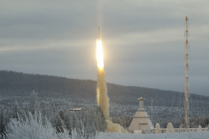
A December 11, 2022 news item on Alarabiya news (and on CNN) describes the ‘graphene’ launch which was also marked the Arab World’s first mission to the moon,

The United Arab Emirates’ Rashid Rover – the Arab world’s first mission to the Moon – was launched on Sunday [December 11, 2022], the Mohammed bin Rashid Space Center (MBRSC) announced on its official Twitter account.

The launch came after it was previously postponed for “pre-flight checkouts.”

The launch of a SpaceX Falcon 9 rocket carrying the UAE’s Rashid rover successfully took off from Cape Canaveral, Florida.

The Rashid rover – built by Emirati engineers from the UAE’s Mohammed bin Rashid Space Center (MBRSC) – is to be sent to regions of the Moon unexplored by humans.

What is the Graphene Flagship?

In 2013, the Graphene Flagship was chosen as one of two FET (Future and Emerging Technologies) funding projects (the other being the Human Brain Project) each receiving €1 billion to be paid out over 10 years. In effect, it’s a science funding programme specifically focused on research, development, and commercialization of graphene (a two-dimensional [it has length and width but no depth] material made of carbon atoms).

You can find out more about the flagship and about graphene here.

Memristive spintronic neurons

A December 6, 2021 news item on Nanowerk on memristive spintronic neurons (Note: A link has been removed),

Researchers at Tohoku University and the University of Gothenburg have established a new spintronic technology for brain-inspired computing.

Their achievement was published in the journal Nature Materials (“Memristive control of mutual SHNO synchronization for neuromorphic computing”).

Sophisticated cognitive tasks, such as image and speech recognition, have seen recent breakthroughs thanks to deep learning. Even so, the human brain still executes these tasks without exerting much energy and with greater efficiency than any computer. The development of energy-efficient artificial neurons capable of emulating brain-inspired processes has therefore been a major research goal for decades.

A November 29, 2021 Tohoku University press release (also on EurekAlert but published November 30, 2021), which originated the news release, provides more technical detail,

Researchers demonstrated the first integration of a cognitive computing nano-element – the memristor – into another – a spintronic oscillator. Arrays of these memristor-controlled oscillators combine the non-volatile local storage of the memristor function with the microwave frequency computation of the nano-oscillator networks and can closely imitate the non-linear oscillatory neural networks of the human brain.

Resistance of the memristor changed with the voltage hysteresis applied to the top Ti/Cu electrode. Upon voltage application to the electrode, an electric field was applied at the high-resistance state, compared to electric current flows for the low-resistance state. The effects of electric field and current on the oscillator differed from each other, offering various controls of oscillation and synchronization properties.

Professor Johan Åkerman of the University of Gothenburg and leader of the study expressed his hopes for the future and the significance of the finding. “We are particularly interested in emerging quantum-inspired computing schemes, such as Ising Machines. The results also highlight the productive collaboration that we have established in neuromorphic spintronics between the University of Gothenburg and Tohoku University, something that is also part of the Sweden-Japan collaborative network MIRAI 2.0.”

“So far, artificial neurons and synapses have been developed separately in many fields; this work marks an important milestone: two functional elements have been combined into one,” said professor Shunsuke Fukami, who led the project on the Tohoku University side. Dr. Mohammad Zahedinejad of the University of Gothenburg and first author of the study adds, “Using the memristor-controlled spintronic oscillator arrays, we could tune the synaptic interactions between adjacent neurons and program them into mutually different and partially synchronized states.”

To put into practice their discovery, the researchers examined the operation of a test device comprising one oscillator and one memristor. The constricted region of W/CoFeB stack served as an oscillator, i.e., the neuron, whereas the MgO/AlOx/SiNx stack acted as a memristor, i.e., the synapse.

Resistance of the memristor changed with the voltage hysteresis applied to the top Ti/Cu electrode. Upon voltage application to the electrode, an electric field was applied at the high-resistance state, compared to electric current flows for the low-resistance state. The effects of electric field and current on the oscillator differed from each other, offering various controls of oscillation and synchronization properties.

Professor Johan Åkerman of the University of Gothenburg and leader of the study expressed his hopes for the future and the significance of the finding. “We are particularly interested in emerging quantum-inspired computing schemes, such as Ising Machines. The results also highlight the productive collaboration that we have established in neuromorphic spintronics between the University of Gothenburg and Tohoku University, something that is also part of the Sweden-Japan collaborative network MIRAI 2.0.” [sic]

Here’s a link to and a citation for the paper,

Memristive control of mutual spin Hall nano-oscillator synchronization for neuromorphic computing by Mohammad Zahedinejad, Himanshu Fulara, Roman Khymyn, Afshin Houshang, Mykola Dvornik, Shunsuke Fukami, Shun Kanai, Hideo Ohno & Johan Åkerman. Nature Materials (2021) DOI: https://doi.org/10.1038/s41563-021-01153-6 Published 29 November 2021

This paper is behind a paywall.

Improving neuromorphic devices with ion conducting polymer

A July 1, 2020 news item on ScienceDaily announces work which researchers are hopeful will allow them exert more control over neuromorphic devices’ speed of response,

“Neuromorphic” refers to mimicking the behavior of brain neural cells. When one speaks of neuromorphic computers, they are talking about making computers think and process more like human brains-operating at high-speed with low energy consumption.

Despite a growing interest in polymer-based neuromorphic devices, researchers have yet to establish an effective method for controlling the response speed of devices. Researchers from Tohoku University and the University of Cambridge, however, have overcome this obstacle through mixing the polymers PSS-Na and PEDOT:PSS, discovering that adding an ion conducting polymer enhances neuromorphic device response time.

A June 24, 2020 Tohoku University press release (also on EurekAlert), which originated the news item, provides a few more technical details,

Polymers are materials composed of long molecular chains and play a fundamental aspect in modern life from the rubber in tires, to water bottles, to polystyrene. Mixing polymers together results in the creation of new materials with their own distinct physical properties.

Most studies on neuromorphic devices based on polymer focus exclusively on the application of PEDOT: PSS, a mixed conductor that transports both electrons and ions. PSS-Na, on the other hand, transports ions only. By blending these two polymers, the researchers could enhance the ion diffusivity in the active layer of the device. Their measurements confirmed an increase in device response time, achieving a 5-time shorting at maximum. The results also proved how closely related response time is to the diffusivity of ions in the active layer.

“Our study paves the way for a deeper understanding behind the science of conducting polymers.” explains co-author Shunsuke Yamamoto from the Department of Biomolecular Engineering at Tohoku University’s Graduate School of Engineering. “Moving forward, it may be possible to create artificial neural networks composed of multiple neuromorphic devices,” he adds.

Here’s a link to and a citation for the paper,

Controlling the Neuromorphic Behavior of Organic Electrochemical Transistors by Blending Mixed and Ion Conductors by Shunsuke Yamamoto and George G. Malliaras. ACS [American Chemical Society] Appl. Electron. Mater. 2020, XXXX, XXX, XXX-XXX DOI: https://doi.org/10.1021/acsaelm.0c00203 Publication Date:June 15, 2020 Copyright © 2020 American Chemical Society

This paper is behind a paywall.

Brainlike computing with spintronic devices

Adding to the body of ‘memristor’ research I have here, there’s an April 17, 2019 news item on Nanowerk announcing the development of ‘memristor’ hardware by Japanese researchers (Note: A link has been removed),

A research group from Tohoku University has developed spintronics devices which are promising for future energy-efficient and adoptive computing systems, as they behave like neurons and synapses in the human brain (Advanced Materials, “Artificial Neuron and Synapse Realized in an Antiferromagnet/Ferromagnet Heterostructure Using Dynamics of Spin–Orbit Torque Switching”).

Just because this ‘synapse’ is pretty,

Courtesy: Tohoku University

An April 16, 2019 Tohoku University press release, which originated the news item, expands on the theme,

Today’s information society is built on digital computers that have evolved drastically for half a century and are capable of executing complicated tasks reliably. The human brain, by contrast, operates under very limited power and is capable of executing complex tasks efficiently using an architecture that is vastly different from that of digital computers.

So the development of computing schemes or hardware inspired by the processing of information in the brain is of broad interest to scientists in fields ranging from physics, chemistry, material science and mathematics, to electronics and computer science.

In computing, there are various ways to implement the processing of information by a brain. Spiking neural network is a kind of implementation method which closely mimics the brain’s architecture and temporal information processing. Successful implementation of spiking neural network requires dedicated hardware with artificial neurons and synapses that are designed to exhibit the dynamics of biological neurons and synapses.

Here, the artificial neuron and synapse would ideally be made of the same material system and operated under the same working principle. However, this has been a challenging issue due to the fundamentally different nature of the neuron and synapse in biological neural networks.

The research group – which includes Professor Hideo Ohno (currently the university president), Associate Professor Shunsuke Fukami, Dr. Aleksandr Kurenkov and Professor Yoshihiko Horio – created an artificial neuron and synapse by using spintronics technology. Spintronics is an academic field that aims to simultaneously use an electron’s electric (charge) and magnetic (spin) properties.

The research group had previously developed a functional material system consisting of antiferromagnetic and ferromagnetic materials. This time, they prepared artificial neuronal and synaptic devices microfabricated from the material system, which demonstrated fundamental behavior of biological neuron and synapse – leaky integrate-and-fire and spike-timing-dependent plasticity, respectively – based on the same concept of spintronics.

The spiking neural network is known to be advantageous over today’s artificial intelligence for the processing and prediction of temporal information. Expansion of the developed technology to unit-circuit, block and system levels is expected to lead to computers that can process time-varying information such as voice and video with a small amount of power or edge devices that have the an ability to adopt users and the environment through usage.

Here’s a link to and a citation for the paper,

Artificial Neuron and Synapse Realized in an Antiferromagnet/Ferromagnet Heterostructure Using Dynamics of Spin–Orbit Torque Switching by Aleksandr Kurenkov, Samik DuttaGupta, Chaoliang Zhang, Shunsuke Fukami, Yoshihiko Horio, Hideo Ohno. Advanced Materials https://doi.org/10.1002/adma.201900636 First published: 16 April 2019

This paper is behind a paywall.

Spintronics-based artificial intelligence

Courtesy: Tohoku University

Japanese researchers have managed to mimic a synapse (artificial neural network) with a spintronics-based device according to a Dec. 19, 2016 Tohoku University press release (also on EurekAlert but dated Dec. 20, 2016),

Researchers at Tohoku University have, for the first time, successfully demonstrated the basic operation of spintronics-based artificial intelligence.

Artificial intelligence, which emulates the information processing function of the brain that can quickly execute complex and complicated tasks such as image recognition and weather prediction, has attracted growing attention and has already been partly put to practical use.

The currently-used artificial intelligence works on the conventional framework of semiconductor-based integrated circuit technology. However, this lacks the compactness and low-power feature of the human brain. To overcome this challenge, the implementation of a single solid-state device that plays the role of a synapse is highly promising.

The Tohoku University research group of Professor Hideo Ohno, Professor Shigeo Sato, Professor Yoshihiko Horio, Associate Professor Shunsuke Fukami and Assistant Professor Hisanao Akima developed an artificial neural network in which their recently-developed spintronic devices, comprising micro-scale magnetic material, are employed (Fig. 1). The used spintronic device is capable of memorizing arbitral values between 0 and 1 in an analogue manner unlike the conventional magnetic devices, and thus perform the learning function, which is served by synapses in the brain.

Using the developed network (Fig. 2), the researchers examined an associative memory operation, which is not readily executed by conventional computers. Through the multiple trials, they confirmed that the spintronic devices have a learning ability with which the developed artificial neural network can successfully associate memorized patterns (Fig. 3) from their input noisy versions just like the human brain can.

The proof-of-concept demonstration in this research is expected to open new horizons in artificial intelligence technology – one which is of a compact size, and which simultaneously achieves fast-processing capabilities and ultralow-power consumption. These features should enable the artificial intelligence to be used in a broad range of societal applications such as image/voice recognition, wearable terminals, sensor networks and nursing-care robots.

Here are Fig. 1 and Fig. 2, as mentioned in the press release,

Fig. 1. (a) Optical photograph of a fabricated spintronic device that serves as artificial synapse in the present demonstration. Measurement circuit for the resistance switching is also shown. (b) Measured relation between the resistance of the device and applied current, showing analogue-like resistance variation. (c) Photograph of spintronic device array mounted on a ceramic package, which is used for the developed artificial neural network. Courtesy: Tohoku University

Fig. 2. Block diagram of developed artificial neural network, consisting of PC, FPGA, and array of spintronics (spin-orbit torque; SOT) devices. Courtesy: Tohoku University

Here`s a link to and a citation for the paper,

Analogue spin–orbit torque device for artificial-neural-network-based associative memory operation by William A. Borders, Hisanao Akima1, Shunsuke Fukami, Satoshi Moriya, Shouta Kurihara, Yoshihiko Horio, Shigeo Sato, and Hideo Ohno. Applied Physics Express, Volume 10, Number 1 https://doi.org/10.7567/APEX.10.013007. Published 20 December 2016

© 2017 The Japan Society of Applied Physics

This is an open access paper.

For anyone interested in my other posts on memristors, artificial brains, and artificial intelligence, you can search this blog for those terms  and/or Neuromorphic Engineering in the Categories section.

Graphene with a pentagonal pattern

Graphene has been viewed, until now, as having an hexgonal (six-sided) pattern. However, researchers have discovered a new graphene pattern according to a Feb. 3, 2015 news item on Nanowerk,

Researchers at Virginia Commonwealth University and universities in China and Japan have discovered a new structural variant of carbon called “penta-graphene” – a very thin sheet of pure carbon that has a unique structure inspired by a pentagonal pattern of tiles found paving the streets of Cairo.

The newly discovered material, called penta-graphene, is a single layer of carbon pentagons that resembles the Cairo tiling, and that appears to be dynamically, thermally and mechanically stable.

A Feb. 3, 2015 Virginia Commonwealth University (VCU) news release by Brian McNeill (also on EurekAlert), which originated the news item, provides more information about the research,

“The three last important forms of carbon that have been discovered were fullerene, the nanotube and graphene. Each one of them has unique structure. Penta-graphene will belong in that category,” said the paper’s senior author, Puru Jena, Ph.D., distinguished professor in the Department of Physics in VCU’s College of Humanities and Sciences.

Qian Wang, Ph.D., a professor at Peking University and an adjunct professor at VCU, was dining in a restaurant in Beijing with her husband when she noticed artwork on the wall depicting pentagon tiles from the streets of Cairo.

“I told my husband, “Come, see! This is a pattern composed only of pentagons,'” she said. “I took a picture and sent it to one of my students, and said, ‘I think we can make this. It might be stable. But you must check it carefully.’ He did, and it turned out that this structure is so beautiful yet also very simple.”

Most forms of carbon are made of hexagonal building blocks, sometimes interspersed with pentagons. Penta-graphene would be a unique two-dimensional carbon allotrope composed exclusively of pentagons.

Along with Jena and Wang, the paper’s authors include Shunhong Zhang, Ph.D candidate, from Peking University; Jian Zhou, Ph.D., a postdoctoral researcher at VCU; Xiaoshuang Chen, Ph.D., from the Chinese Academy of Science in Shanghai; and Yoshiyuki Kawazoe, Ph.D., from Tohoku University in Sendai, Japan.

The researchers simulated the synthesis of penta-graphene using computer modelling. The results suggest that the material might outperform graphene in certain applications, as it would be mechanically stable, possess very high strength, and be capable of withstanding temperatures of up to 1,000 degrees Kelvin.

“You know the saying, diamonds are forever? That’s because it takes a lot of energy to convert diamond back into graphite,” Jena said. “This will be similar.”

Penta-graphene has several interesting and unusual properties, Jena said. For example, penta-graphene is a semiconductor, whereas graphene is a conductor of electricity.

“When you take graphene and roll it up, you make what is called a carbon nanotube which can be metallic or semiconducting,” Jena said. “Penta-graphene, when you roll it up, will also make a nanotube, but it is always semiconducting.”

The way the material stretches is also highly unusual, the researchers said.

“If you stretch graphene, it will expand along the direction it is stretched, but contract along the perpendicular direction.” Wang said. “However, if you stretch penta-graphene, it will expand in both directions.”

The material’s mechanical strength, derived from a rare property known as Negative Poisson’s Ratio, may hold especially interesting applications for technology, the researchers said.

Penta-graphene’s properties suggest that it may have applications in electronics, biomedicine, nanotechnology and more.

The next step, Jena said, is for scientists to synthesize penta-graphene.

“Once you make it, it [will be] very stable. So the question becomes, how do you make it? In this paper, we have some ideas. Right now, the project is theoretical. It’s based on computer modelling, but we believe in this prediction quite strongly. And once you make it, it will open up an entirely new branch of carbon science. Two-dimensional carbon made completely of pentagons has never been known.”

Here’s a graphic representation of the new graphene material,

Caption: The newly discovered material, called penta-graphene, is a single layer of carbon pentagons that resembles the Cairo tiling, and that appears to be dynamically, thermally and mechanically stable. Credit: Virginia Commonwealth University

Caption: The newly discovered material, called penta-graphene, is a single layer of carbon pentagons that resembles the Cairo tiling, and that appears to be dynamically, thermally and mechanically stable.
Credit: Virginia Commonwealth University

Here’s a link to and a citation for the paper,

Penta-graphene: A new carbon allotrope by Shunhong Zhanga, Jian Zhou, Qian Wanga, Xiaoshuang Chen, Yoshiyuki Kawazoe, and Puru Jena. PNAS February 2, 2015 doi: 10.1073/pnas.1416591112 Published online before print February 2, 2015

This paper is behind a paywall.

Institute of Electrical and Electronics Engineers (IEEE) 2014 international nanotechnology conference in Toronto, Canada

August 18 – 21, 2014 are the dates for the IEEE (Institute for Electrical and Electronics Engineers) 14th International Conference on Nanotechnology.  The deadline for submitting abstracts is March 15, 2014. Here’s a bit more about the conference, from the homepage,

IEEE Nano is one of the largest Nanotechnology conferences in the world, bringing together the brightest engineers and scientists through collaboration and the exchange of ideas.

IEEE Nano 2014 will provide researchers and others in the Nanotechnology field the ability to interact and advance their work through various speakers and workshop sessions.

Possible Topics for Papers

Environmental Health and Safety of Nanotechnology
Micro-to-nano-scale bridging
Modeling and Simulation
Nanobiology:
•Nanobiomedicine
•Nanobiosystems
•Applications of Biopolymer Nanoparticles for Drug Delivery
Nanoelectronics:
•Non-Carbon Based
•Carbon Based
•Circuits and Architecture
Nanofabrication and Nanoassemblies
Nanofluidics:
•Modeling and Theory
•Applications
Nanomagnetics
Nanomanufacturing
Nanomaterials:
•2-D Materials beyond Graphene
•Synthesis and Characterization
•Applications and Enabled Systems
Nanometrology and Nanocharacterization
Nanopackaging
Nano-optics, Nano-optoelectronics and Nano-photonics:
•Novel fabrication and integration approaches
•Optical Nano-devices
Nanorobotics and Nanomanipulation
Nanoscale Communication and Networks
Nanosensors and Actuators
Nanotechnology Enabled Energy
NEMS
NEMS/Applications

There is a conference Call For Papers webpage where you can get more information.

Invited speakers include,

John Polanyi
Professor
University of Toronto, Canada

John Polanyi, educated at Manchester University, England, was a postdoctoral fellow at Princeton University and at the National Research Council of Canada. He is a faculty member in the Department of Chemistry at the University of Toronto, a member of the Queen’s Privy Council for Canada (P.C.), and a Companion of the Order of Canada (C.C.). His awards include the 1986 Nobel Prize in Chemistry. He has written extensively on science policy, the control of armaments, peacekeeping and human rights.

Charles Lieber
Professor Charles M. Lieber
Mark Hyman Professor of Chemistry
Department of Chemistry and Chemical Biology
Harvard University

Charles M. Lieber is regarded as a leading chemist worldwide and recognized as a pioneer in the nanoscience and nanotechnology fields. He completed his doctoral studies at Stanford University and currently holds a joint appointment in the Department of Chemistry and Chemical Biology at Harvard University, as the Mark Hyman Professor of Chemistry, and the School of Engineering and Applied Sciences. Lieber is widely known for his contributions to the synthesis, understanding and assembly of nanoscale materials, as well as the founding of two nanotechnology companies: Nanosys and Vista Therapeutics.

Lieber’s achievements have been recognized by a large number of awards, including the Feynman Prize for Nanotechnology (2002), World Technology award in Materials (2003 and 2004) and the Wolf Prize in Chemistry (2012). He has published more than 350 papers in peer-reviewed journals and is the primary inventor on over 35 patents.

Arthur Carty
Professor & Executive Director [Waterloo Institute for Nanotechnology]
University of Waterloo, Canada

Arthur Carty has a PhD in inorganic chemistry from the University of Nottingham in the UK. He is currently the Executive Director of the Waterloo Institute for Nanotechnology and research professor in the Department of Chemistry at the University of Waterloo.

Previously, Dr. Carty served in Canada as the National Science Advisor to the Prime Minister and President of the National Research Council (Canada). He was awarded the Order of Canada and holds 14 honorary doctorates.

His research interests are focused on organometallic chemistry and new materials. [Dr. Carty is chair of The Expert Panel on the State of Canada’s Science Culture; an assessment being conducted by the Canadian Council of Academies as per my Feb. 22, 2013 posting and Dr. Carty is giving a Keynote lecture titled: ‘Small World, Large Impact: Driving a Materials Revolution Through Nanotechnology’ at the 2014 TAPPI (Technical Association for the Pulp, Paper, Packaging and Converting Industries) nanotechnology conference, June 23-26, 2014 in Vancouver, Canada as per my Nov. 14, 2013 posting.]

William Milne
Professor
University of Cambridge, UK

Bill Milne FREng,FIET,FIMMM has been Head of Electrical Engineering at Cambridge University since 1999 and Director of the Centre for Advanced Photonics and Electronics (CAPE) since 2005. In 1996 he was appointed to the ‘‘1944 Chair in Electrical Engineering’’. He obtained his BSc from St Andrews University in Scotland in 1970 and then went on to read for a PhD in Electronic Materials at Imperial College London. He was awarded his PhD and DIC in 1973 and, in 2003, a D.Eng (Honoris Causa) from University of Waterloo, Canada. He was elected a Fellow of The Royal Academy of Engineering in 2006. He was awarded the J.J. Thomson medal from the IET in 2008 and the NANOSMAT prize in 2010 for excellence in nanotechnology. His research interests include large area Si and carbon based electronics, graphene, carbon nanotubes and thin film materials. Most recently he has been investigating MEMS, SAW and FBAR devices and SOI based micro heaters for ( bio) sensing applications. He has published/presented ~ 800 papers in these areas, of which ~ 150 were invited. He co-founded Cambridge Nanoinstruments with 3 colleagues from the Department and this was bought out by Aixtron in 2008 and in 2009 co-founded Cambridge CMOS Sensors with Julian Gardner from Warwick Univ. and Florin Udrea from Cambridge Univ.

Shuit-Tong Lee
Institute of Functional Nano & Soft Materials (FUNSOM)
Collaboration Innovation Center of Suzhou Nano Science and Technology
College of Nano Science and Technology (CNST)
Soochow University, China
Email: apannale@suda.edu.c

Prof. Lee is the member (academician) of Chinese Academy of Sciences and the fellow of TWAS (the academy of sciences for the developing world). He is a distinguished scientist in material science and engineering. Prof. Lee is the Founding Director of Functional Nano & Soft Materials Laboratory (FUNSOM) and Director of the College of Chemistry, Chemical Engineering and Materials Science at Soochow University. He is also a Chair Professor of Materials Science and Founding Director of the Center of Super-Diamond and Advanced Films (COSDAF) at City University of Hong Kong and the Founding Director of Nano-Organic Photoelectronic Laboratory at the Technical Institute of Physics and Chemistry, CAS. He was the Senior Research Scientist and Project Manager at the Research Laboratories of Eastman Kodak Company in the US before he joined City University of Hong Kong in 1994. He won the Humboldt Senior Research Award (Germany) in 2001 and a Croucher Senior Research Fellowship from the Croucher Foundation (HK) in 2002 for the studies of “Nucleation and growth of diamond and new carbon based materials” and “Oxide assisted growth and applications of semiconducting nanowires”, respectively. He also won the National Natural Science Award of PRC (second class) in 2003 and 2005 for the above research achievements. Recently, he was awarded the 2008 Prize for Scientific and Technological Progress of Ho Leung Ho Lee Foundation. Prof. Lee’s research work has resulted in more than 650 peer-reviewed publications in prestigious chemistry, physics and materials science journals, 6 book chapters and over 20 US patents, among them 5 papers were published in Science and Nature (London) and some others were selected as cover papers. His papers have more than 10,000 citations by others, which is ranked within world top 25 in the materials science field according to ESI and ISI citation database.

Sergej Fatikow
Full Professor, Dr.-Ing. habil.
Head, Division for Microrobotics & Control Engineering (AMiR)
University of Oldenburg, Germany

Professor Sergej Fatikow studied electrical engineering and computer science at the Ufa Aviation Technical University in Russia, where he received his doctoral degree in 1988 with work on fuzzy control of complex non-linear systems. After that he worked until 1990 as a lecturer at the same university. During his work in Russia he published over 30 papers and successfully applied for over 50 patents in intelligent control and mechatronics. In 1990 he moved to the Institute for Process Control and Robotics at the University of Karlsruhe in Germany, where he worked as a postdoctoral scientific researcher and since 1994 as Head of the research group “Microrobotics and Micromechatronics”. He became an assistant professor in 1996 and qualified for a full faculty position by habilitation at the University of Karlsruhe in 1999. In 2000 he accepted a faculty position at the University of Kassel, Germany. A year later, he was invited to establish a new Division for Microrobotics and Control Engineering (AMiR) at the University of Oldenburg, Germany. Since 2001 he is a full professor in the Department of Computing Science and Head of AMiR. His research interests include micro- and nanorobotics, automated robot-based nanohandling in SEM, AFM-based nanohandling, sensor feedback at nanoscale, and neuro-fuzzy robot control. He is author of three books on microsystem technology, microrobotics and microassembly, robot-based nanohandling, and automation at nanoscale, published by Springer in 1997, Teubner in 2000, and Springer in 2008. Since 1990 he published over 100 book chapters and journal papers and over 200 conference papers. Prof. Fatikow is Founding Chair of the International Conference on Manipulation, Manufacturing and Measurement on the Nanoscale (3M-NANO) and Europe- Chair of IEEE-RAS Technical Committee on Micro/Nano Robotics and Automation.

Seiji Samukawa
Distinguished Professor
Innovative Energy Research Center, Institute of Fluid Science, Tohoku University
World Premier International Center Initiative, Advanced Institute for Materials Research, Tohoku University, Sendai, Japan

Dr. Seiji Samukawa received a BSc in 1981 from the Faculty of Technology of Keio University and joined NEC Corporation the same year. At NEC Microelectronics Research Laboratories, he was the lead researcher of a group performing fundamental research on advanced plasma etching processes for technology under 0.1 μm. While there, he received the Ishiguro Award—given by NEC’s R&D Group and Semiconductor Business Group— for his work in applying a damage-free plasma etching process to a mass-production line. After spending several years in the business world, however, he returned to Keio University, obtaining a PhD in engineering in 1992. Since 2000, he has served as professor at the Institute of Fluid Science at Tohoku University and developed ultra-low-damage microfabrication techniques that tap into the essential nature of nanomaterials and developed innovative nanodevices. He is also carrying out pioneering, creative research on bio-template technologies, which are based on a completely new concept of treating the super-molecules of living organisms. His motto when conducting research is to “always aim toward eventual practical realization.”

In recognition of his excellent achievements outlined above, he has been elected as a Distinguished Professor of Tohoku University and has been a Fellow of the Japan Society of Applied Physics since 2008 and a Fellow of the American Vacuum Society since 2009. His significant scientific achievements earned him the Outstanding Paper Award at the International Conference on Micro and Nanotechnology (1997), Best Review Paper Award (2001), Japanese Journal of Applied Physics (JJAP) Editorial Contribution Award (2003), Plasma Electronics Award (2004), Fellow Award (2008), JJAP Paper Award (2008) from the Japan Society of Applied Physics, Distinguished Graduate Award (2005) from Keio University, Ichimura Award (2008) from the New Technology Development Foundation, Commendation for Science and Technology from the Minister of Education, Culture, Sports, Science and Technology (2009), Fellow Award of American Vacuum Society (2009), Plasma Electronics Award from the Japan Society of Applied Physics (2010), Best Paper Award from the Japan Society of Applied Physics (2010), and Plasma Prize from the Plasma Science and Technology Division of American Vacuum Society (2010).

Haixia (Alice) Zhang
Professor
Institute of Microelectronics
Peking University, China

Haixia(Alice) Zhang, Professor, Institute of Microelectronics, Peking Universituy. She was served on the general chair of IEEE NEMS 2013 Conference, the organizing chair of Transducers’11. As the founder of the International Contest of Applications in Network of things (iCAN), she organized this world-wide event since 2007. She was elected the director of Integrated Micro/Nano System Engineering Center in 2006, the deputy secretary-general of Chinese Society of Micro-Nano Technology in 2005, the Co-chair of Chinese International NEMS Network (CINN) and serves as the chair of IEEE NTC Beijing Chapter. At 2006, Dr. Zhang won National Invention Award of Science & Technology. Her research fields include MEMS Design and Fabrication Technology, SiC MEMS and Micro Energy Technology.

Alice’s Wonderlab: http://www.ime.pku.edu.cn/alice

I wonder if the organizers will be including an Open Forum as they did at the 13th IEEE nanotechnology conference in China. It sounds a little more dynamic and fun than any of the sessions currently listed for the Toronto conference but these things are sometimes best organized in a relatively spontaneous fashion rather than as one of the more formal conference events (from the 13th conference Open Forum),

This Open Forum will be run like a Rump Session to have a lively discussion of various topics of interest to the IEEE Nanotechnology Community. The key to the success of this Forum is participation from the audience with their own opinions and comments on any Nanotechnology subject or issue they can think of. We expect the session to be lively, interesting, controversial, opinionated and more. Here are some topics or issues to think about:

  1. When are we ever going to have a large scale impact of nanotechnology ? Shouldn’t we be afraid that the stakeholders (Tax payers, Politicians) are going to run out of patience ?
  2. Is there a killer app or apps on the horizon ?
  3. Is there a future for carbon nanotubes in electronics ? It has been 15 years + now….
  4. Is there a future for graphene in electronics ?
  5. Is there a future for graphene in anything ? Or will it just run its course on every application people did previously for carbon nanotubes ?
  6. As engineers, are we doing anything different from the physicists/chemists ? Looks like we are also chasing the same old : trying to publish in Nature, Science, and other similar journals with huge impact factor ? Are we prepared adequately to play in someone else’s game ? Should we even be doing it ?
  7. As engineers, aren’t we supposed to come up with working widgets closer to manufacturing ?
  8. As engineers, are we going to take responsibility for the commercial future of nanotechnology as has been done in all previous success stories ?

This list is by no means exhaustive. Please come up with your own questions/issues and speak up at the session.

Good luck with your abstract.

Single-element quasicrystal created in laboratory for the first time

There’s a background story which gives this breakthrough a fabulous aspect but, first, here’s the research breakthrough from a Dec. 24, 2013 news item on Nanowerk (Note: A link has been removed),

A research group led by Assistant Professor Kazuki Nozawa and Professor Yasushi Ishii from the Department of Physics, Faculty of Science and Engineering, Chuo University, Chief Researcher Masahiko Shimoda from the National Institute for Materials Science (NIMS) and Professor An-Pang Tsai from the Institute of Multidisciplinary Research for Advanced Materials (IMRAM), Tohoku University, succeeded for the first time in the world in fabricating a three-dimensional structure of a quasicrystal composed of a single element, through joint research with a group led by Dr. Hem Raj Sharma from the University of Liverpool, the United Kingdom.

The Dec. 2, 2013 National Institute for Materials Science (NIMS; Japan) press release, which originated the news item, describes quasicrystals and the reasons why this particular achievement is such a breakthrough,

Quasicrystals are substances discovered in 1984 by Dr. Dan Shechtman (who was awarded the Nobel Prize in Chemistry in 2011). [emphasis mine] To date, quasicrystals have been found in more than one hundred kinds of alloy, polymer and nanoparticle systems. However, a quasicrystal composed of a single element has not been found yet. Quasicrystals have a beautiful crystalline structure which is closely related to the golden ratio, called a quasiperiodic structure. This structure is made of a pentagonal or decagonal atomic arrangement that is not found in ordinary periodic crystals (see the reference illustrations). Due to the complexity of the crystalline structure and chemical composition, much about quasicrystals is still veiled in mystery, including the mechanism for stabilizing a quasiperiodic structure and the novel properties of this unique type of crystalline structure. For these reasons, efforts have been made for a long time in the quest for a chemically simple type of quasicrystal composed only of a single element. The joint research group has recently succeeded in growing a crystal of lead with a quasiperiodic structure which is modeled on the structure of a substrate quasicrystal, by vapor-depositing lead atoms on the quasicrystal substrate of an existing alloy made of silver (Ag), indium (In) and ytterbium (Yb). Success using this approach had been reported for fabricating a single-element quasiperiodic film consisting of a single atomic layer (two-dimensional structure), but there had been no successful case of fabricating a single-element quasiperiodic structure consisting of multiple atomic layers (three-dimensional structure). This recent success by the joint research group is a significant step forward toward achieving single-element quasicrystals. It is also expected to lead to advancement in various fields, such as finding properties unique to quasiperiodic structures that cannot be found in periodic crystals and elucidating the mechanism of stabilization of quasiperiodic structures.

Here’s an image illustrating the researchers’ achievement,

Illustrations of the deposition structure of lead. The Tsai cluster in the substrate quasicrystal which is near the surface of the substrate is cut at the point where it contacts the surface. While lead usually has a face-centered cubic structure, it is deposited on the quasicrystal substrate in a manner that it recovers Tsai clusters which are cut near the surface of the substrate. This indicates that a crystal of lead is grown with the same structure as the structure of the quasicrystal substrate. (Courtesy National Institute for Materials Science, Japan)

Illustrations of the deposition structure of lead. The Tsai cluster in the substrate quasicrystal which is near the surface of the substrate is cut at the point where it contacts the surface. While lead usually has a face-centered cubic structure, it is deposited on the quasicrystal substrate in a manner that it recovers Tsai clusters which are cut near the surface of the substrate. This indicates that a crystal of lead is grown with the same structure as the structure of the quasicrystal substrate. (Courtesy National Institute for Materials Science, Japan)

I suggested earlier that this achievement has a fabulous quality and the Daniel Schechtman backstory is the reason. The winner of the 2011 Nobel Prize for Chemistry, Schechtman was reviled for years within his scientific community as Ian Sample notes in his Oct. 5, 2011 article on the announcement of Schechtman’s Nobel win written for the Guardian newspaper (Note: A link has been removed),

A scientist whose work was so controversial he was ridiculed and asked to leave his research group has won the Nobel Prize in Chemistry.

Daniel Shechtman, 70, a researcher at Technion-Israel Institute of Technology in Haifa, received the award for discovering seemingly impossible crystal structures in frozen gobbets of metal that resembled the beautiful patterns seen in Islamic mosaics.

Images of the metals showed their atoms were arranged in a way that broke well-establised rules of how crystals formed, a finding that fundamentally altered how chemists view solid matter.

On the morning of 8 April 1982, Shechtman saw something quite different while gazing at electron microscope images of a rapidly cooled metal alloy. The atoms were packed in a pattern that could not be repeated. Shechtman said to himself in Hebrew, “Eyn chaya kazo,” which means “There can be no such creature.”

The bizarre structures are now known as “quasicrystals” and have been seen in a wide variety of materials. Their uneven structure means they do not have obvious cleavage planes, making them particularly hard.

In an interview this year with the Israeli newspaper, Haaretz, Shechtman said: “People just laughed at me.” He recalled how Linus Pauling, a colossus of science and a double Nobel laureate, mounted a frightening “crusade” against him. After telling Shechtman to go back and read a crystallography textbook, the head of his research group asked him to leave for “bringing disgrace” on the team. “I felt rejected,” Shachtman said.

It takes a lot to persevere when most, if not all, of your colleagues are mocking and rejecting your work so bravo to Schechtman! And,bravo to the Japan-UK project researchers who have persevered to help solve at least part of a complex problem requiring that our basic notions of matter be rethought.

I encourage you to read Sample’s article in its entirety as it is well written and I’ve excerpted only bits of the story as it relates to a point I’m making in this post, i.e., perseverance in the face of extreme resistance.

Should October 2013 be called ‘the month of graphene’?

Since the Oct. 10-11, 2013 Graphene Flagship (1B Euros investment) launch, mentioned in my preview Oct. 7, 2013 posting, there’ve been a flurry of graphene-themed news items both on this blog and elsewhere and I’ve decided to offer a brief roundup what I’ve found elsewhere.

Dexter Johnson offers a commentary in the pithily titled, Europe Invests €1 Billion to Become “Graphene Valley,” an Oct. 15, 2013 posting on his Nanoclast blog (on the IEEE [Institute of Electrical and Electronics Engineers] website) Note: Links have been removed,

The initiative has been dubbed “The Graphene Flagship,” and apparently it is the first in a number of €1 billion, 10-year plans the EC is planning to launch. The graphene version will bring together 76 academic institutions and industrial groups from 17 European countries, with an initial 30-month-budget of €54M ($73 million).

Graphene research is still struggling to find any kind of applications that will really take hold, and many don’t expect it will have a commercial impact until 2020. What’s more, manufacturing methods are still undeveloped. So it would appear that a 10-year plan is aimed at the academic institutions that form the backbone of this initiative rather than commercial enterprises.

Just from a political standpoint the choice of Chalmers University in Sweden as the base of operations for the Graphene Flagship is an intriguing choice. …

I have to agree with Dexter that choosing Chalmers University over the University of Manchester where graphene was first isolated is unexpected. As a companion piece to reading Dexter’s posting in its entirety and which features a video from the flagship launch, you might want to try this Oct. 15, 2013 article by Koen Mortelmans for Youris (h/t Oct. 15, 2013 news item on Nanowerk),

Andre Konstantin Geim is the only person who ever received both a Nobel and an Ig Nobel. He was born in 1958 in Russia, and is a Dutch-British physicist with German, Polish, Jewish and Ukrainian roots. “Having lived and worked in several European countries, I consider myself European. I don’t believe that any further taxonomy is necessary,” he says. He is now a physics professor at the University of Manchester. …

He shared the Noble [Nobel] Prize in 2010 with Konstantin Novoselov for their work on graphene. It was following on their isolation of microscope visible grapheme flakes that the worldwide research towards practical applications of graphene took off.  “We did not invent graphene,” Geim says, “we only saw what was laid up for five hundred year under our noses.”

Geim and Novoselov are often thought to have succeeded in separating graphene from graphite by peeling it off with ordinary duct tape until there only remained a layer. Graphene could then be observed with a microscope, because of the partial transparency of the material. That is, after dissolving the duct tape material in acetone, of course. That is also the story Geim himself likes to tell.

However, he did not use – as the urban myth goes – graphite from a common pencil. Instead, he used a carbon sample of extreme purity, specially imported. He also used ultrasound techniques. But, probably the urban legend will survive, as did Archimedes’ bath and Newtons apple. “It is nice to keep some of the magic,” is the expression Geim often uses when he does not want a nice story to be drowned in hard facts or when he wants to remain discrete about still incomplete, but promising research results.

Mortelmans’ article fills in some gaps for those not familiar with the graphene ‘origins’ story while Tim Harper’s July 22, 2012 posting on Cientifica’s (an emerging technologies consultancy where Harper is the CEO and founder) TNT blog offers an insight into Geim’s perspective on the race to commercialize graphene with a paraphrased quote for the title of Harper’s posting, “It’s a bit silly for society to throw a little bit of money at (graphene) and expect it to change the world.” (Note: Within this context, mention is made of the company’s graphene opportunities report.)

With all this excitement about graphene (and carbon generally), the magazine titled Carbon has just published a suggested nomenclature for 2D carbon forms such as graphene, graphane, etc., according to an Oct. 16, 2013 news item on Nanowerk (Note: A link has been removed),

There has been an intense research interest in all two-dimensional (2D) forms of carbon since Geim and Novoselov’s discovery of graphene in 2004. But as the number of such publications rise, so does the level of inconsistency in naming the material of interest. The isolated, single-atom-thick sheet universally referred to as “graphene” may have a clear definition, but when referring to related 2D sheet-like or flake-like carbon forms, many authors have simply defined their own terms to describe their product.

This has led to confusion within the literature, where terms are multiply-defined, or incorrectly used. The Editorial Board of Carbon has therefore published the first recommended nomenclature for 2D carbon forms (“All in the graphene family – A recommended nomenclature for two-dimensional carbon materials”).

This proposed nomenclature comes in the form of an editorial, from Carbon (Volume 65, December 2013, Pages 1–6),

All in the graphene family – A recommended nomenclature for two-dimensional carbon materials

  • Alberto Bianco
    CNRS, Institut de Biologie Moléculaire et Cellulaire, Immunopathologie et Chimie Thérapeutique, Strasbourg, France
  • Hui-Ming Cheng
    Shenyang National Laboratory for Materials Science, Institute of Metal Research, Chinese Academy of Sciences, 72 Wenhua Road, Shenyang 110016, China
  • Toshiaki Enoki
    Department of Chemistry, Graduate School of Science and Engineering, Tokyo Institute of Technology, Tokyo, Japan
  • Yury Gogotsi
    Materials Science and Engineering Department, A.J. Drexel Nanotechnology Institute, Drexel University, 3141 Chestnut Street, Philadelphia, PA 19104, USA
  • Robert H. Hurt
    Institute for Molecular and Nanoscale Innovation, School of Engineering, Brown University, Providence, RI 02912, USA
  • Nikhil Koratkar
    Department of Mechanical, Aerospace and Nuclear Engineering, The Department of Materials Science and Engineering, Rensselaer Polytechnic Institute, 110 8th Street, Troy, NY 12180, USA
  • Takashi Kyotani
    Institute of Multidisciplinary Research for Advanced Materials, Tohoku University, 2-1-1 Katahira, Aoba-ku, Sendai 980-8577, Japan
  • Marc Monthioux
    Centre d’Elaboration des Matériaux et d’Etudes Structurales (CEMES), UPR-8011 CNRS, Université de Toulouse, 29 Rue Jeanne Marvig, F-31055 Toulouse, France
  • Chong Rae Park
    Carbon Nanomaterials Design Laboratory, Global Research Laboratory, Research Institute of Advanced Materials, Department of Materials Science and Engineering, Seoul National University, Seoul 151-744, Republic of Korea
  • Juan M.D. Tascon
    Instituto Nacional del Carbón, INCAR-CSIC, Apartado 73, 33080 Oviedo, Spain
  • Jin Zhang
    Center for Nanochemistry, College of Chemistry and Molecular Engineering, Peking University, Beijing 100871, China

This editorial is behind a paywall.

Germany goes international with SpinNet, its spintronics project

A Feb. 8, 2013 news item on Nanowerk features an announcement of an international spintronics project, SpinNet, being funded by the federal government of Germany,

The German Academic Exchange Service (DAAD) is sponsoring a joint project involving Johannes Gutenberg University Mainz (JGU) in Mainz, Tohoku University in Japan, Stanford University, and IBM Research. The project will be focusing on the field of spintronics, a key technology that enables the creation of new energy-efficient IT devices. At Mainz researchers from JGU’s Institute of Physics and the Institute of Inorganic Chemistry and Analytical Chemistry participate with many of the activities taking place under the Materials Science in Mainz (MAINZ) Graduate School of Excellence. Over the next four years, the SpinNet network will be funded with about EUR 1 million from the German Federal Ministry of Education and Research (BMBF). SpinNet is one of the 21 projects that the German Academic Exchange Service approved from the total of 120 proposals submitted in the first round and from the 40 entries that made it to the second round.

The Johannes Gutenberg-Universität Mainz (Mainz University) Feb. 8, 2013 news release, which originated the news item, provides details about the network and about the project itself,

Under the aegis of the MAINZ Graduate School, Johannes Gutenberg University Mainz had submitted a proposal for financial support as a so-called “Thematic Network”. With this program, the German Academic Exchange Service aims to provide support to research-based multilateral and international networks with leading partners from abroad. The inclusion of non-university research facilities, such as IBM Research, was encouraged and the program is intended to help create attractive conditions that will help attract excellent international young researchers from partner universities to Germany. Another purpose is to enable the participating German universities to work at the cutting edge of international research by creating centers of competence. The MAINZ Graduate School has been closely cooperating with the partners for years and SpinNet will help to further this cooperation and fund complementary activities.

SpinNet will concentrate on the development of energy-saving information technology using the potential provided by spintronics. The current semiconductor-based systems will reach their limits in the foreseeable future, meaning that innovative technologies need to be developed if components are to be miniaturized further and energy consumption is reduced. In this context, spintronics is a highly promising approach. While conventional electronic systems in IT components employ only the charge of electrons, spintronics also involves the intrinsic angular momentum or spin of electrons for information processing. Using this technology, it should be possible to develop non-volatile storage and logic systems and these would then reduce energy consumption while also radically simplifying systems architecture. The new research network will be officially launched on April 1, 2013; with the inaugural meeting of the partners taking place at the Newspin3 Conference that is to be held on April 2-4, 2013 in Mainz.

You can find more information and videos about this initiative and/or spintronics by clicking the news item link or news release link.  There does not seem to be a SpinNet website. NewsSpin3 conference information can be found here along with details about the NewSpin3 summer school which takes place immediately following the conference. Spintronics was last mentioned here in a Jan. 31, 2013 posting about a 3-D microchip developed from a spintronics chip.