Tag Archives: Koen Mortelmans

Historic and other buildings get protection from pollution?

This Sept. 15, 2017 news item on Nanowerk announces a new product for protecting buildings from pollution,

The organic pollution decomposing properties of titanium dioxide (TiO2 ) have been known for about half a century. However, practical applications have been few and hard to develop, but now a Greek paint producer claims to have found a solution

A Sept. 11, 2017 Youris (European Research Media Center) press release by Koen Mortelmans which originated the news item expands on the theme,

The photocatalytic properties of anatase, one of the three naturally occurring forms of titanium dioxide, were discovered in Japan in the late 1960s. Under the influence of the UV-radiation in sunlight, it can decompose organic pollutants such as bacteria, fungi and nicotine, and some inorganic materials into carbon dioxide. The catalytic effect is caused by the nanostructure of its crystals.

Applied outdoors, this affordable and widely available material could represent an efficient self-cleaning solution for buildings. This is due to the chemical reaction, which leaves a residue on building façades, a residue then washed away when it rains. Applying it to monuments in urban areas may save our cultural heritage, which is threatened by pollutants.

However, “photocatalytic paints and additives have long been a challenge for the coating industry, because the catalytic action affects the durability of resin binders and oxidizes the paint components,” explains Ioannis Arabatzis, founder and managing director of NanoPhos, based in the Greek town of Lavrio, in one of the countries home to some of the most important monuments of human history. The Greek company is testing a paint called Kirei, inspired by a Japanese word meaning both clean and beautiful.

According to Arabatzis, it’s an innovative product because it combines the self-cleaning action of photocatalytic nanoparticles and the reflective properties of cool wall paints. “When applied on exterior surfaces this paint can reflect more than 94% of the incident InfraRed radiation (IR), saving energy and reducing costs for heating and cooling”, he says. “The reflection values are enhanced by the self-cleaning ability. Compared to conventional paints, they remain unchanged for longer.”

The development of Kirei has been included in the European project BRESAER (BREakthrough Solutions for Adaptable Envelopes in building Refurbishment) which is studying a sustainable and adaptable “envelope system” to renovate buildings. The new paint was tested and subjected to quality controls following ISO standard procedures at the company’s own facilities and in other independent laboratories. “The lab results from testing in artificial, accelerated weathering conditions are reliable,” Arabatzis claims. “There was no sign of discolouration, chalking, cracking or any other paint defect during 2,000 hours of exposure to the simulated environmental conditions. We expect the coating’s service lifetime to be at least ten years.”

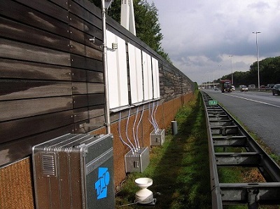
Many studies are being conducted to exploit the properties of titanium dioxide. Jan Duyzer, researcher at the Netherlands Organisation for Applied Scientific Research (TNO) in Utrecht, focused on depollution: “There is no doubt about the ability of anatase to decrease the levels of nitrogen oxides in the air. But in real situations, there are many differences in pollution, wind, light, and temperature. We were commissioned by the Dutch government specifically to find a way to take nitrogen oxides out of the air on roads and in traffic tunnels. We used anatase coated panels. Our results were disappointing, so the government decided to discontinue the research. Furthermore, we still don’t know what caused the difference between lab and life. Our best current hypothesis is that the total surface of the coated panels is very small compared to the large volumes of polluted air passing over them,” he tells youris.com.

Experimental deployment of titanium dioxide panels on an acoustic wall along a Dutch highway – Courtesy of Netherlands Organisation for Applied Scientific Research (TNO)

“In laboratory conditions the air is blown over the photocatalytic surface with a certain degree of turbulence. This results in the NOx-particles and the photocatalytic material coming into full contact with one another,” says engineer Anne Beeldens, visiting professor at KU Leuven, Belgium. Her experience with photocatalytic TiO2 is also limited to nitrogen dioxide (NOx) pollution.

In real applications, the air stream at the contact surface becomes laminar. This results in a lower velocity of the air at the surface and a lower depollution rate. Additionally, not all the air will be in contact with the photocatalytic surfaces. To ensure a good working application, the photocatalytic material needs to be positioned so that all the air is in contact with the surface and flows over it in a turbulent manner. This would allow as much of the NOx as possible to be in contact with photocatalytic material. In view of this, a good working application could lead to a reduction of 5 to 10 percent of NOx in the air, which is significant compared to other measures to reduce pollutants.”

The depollution capacity of TiO2 is undisputed, but most applications and tests have only involved specific kinds of substances. More research and measurements are required if we are to benefit more from the precious features of this material.

I think the most recent piece here on protecting buildings, i.e., the historic type, from pollution is an Oct. 21, 2014 posting: Heart of stone.

Should October 2013 be called ‘the month of graphene’?

Since the Oct. 10-11, 2013 Graphene Flagship (1B Euros investment) launch, mentioned in my preview Oct. 7, 2013 posting, there’ve been a flurry of graphene-themed news items both on this blog and elsewhere and I’ve decided to offer a brief roundup what I’ve found elsewhere.

Dexter Johnson offers a commentary in the pithily titled, Europe Invests €1 Billion to Become “Graphene Valley,” an Oct. 15, 2013 posting on his Nanoclast blog (on the IEEE [Institute of Electrical and Electronics Engineers] website) Note: Links have been removed,

The initiative has been dubbed “The Graphene Flagship,” and apparently it is the first in a number of €1 billion, 10-year plans the EC is planning to launch. The graphene version will bring together 76 academic institutions and industrial groups from 17 European countries, with an initial 30-month-budget of €54M ($73 million).

Graphene research is still struggling to find any kind of applications that will really take hold, and many don’t expect it will have a commercial impact until 2020. What’s more, manufacturing methods are still undeveloped. So it would appear that a 10-year plan is aimed at the academic institutions that form the backbone of this initiative rather than commercial enterprises.

Just from a political standpoint the choice of Chalmers University in Sweden as the base of operations for the Graphene Flagship is an intriguing choice. …

I have to agree with Dexter that choosing Chalmers University over the University of Manchester where graphene was first isolated is unexpected. As a companion piece to reading Dexter’s posting in its entirety and which features a video from the flagship launch, you might want to try this Oct. 15, 2013 article by Koen Mortelmans for Youris (h/t Oct. 15, 2013 news item on Nanowerk),

Andre Konstantin Geim is the only person who ever received both a Nobel and an Ig Nobel. He was born in 1958 in Russia, and is a Dutch-British physicist with German, Polish, Jewish and Ukrainian roots. “Having lived and worked in several European countries, I consider myself European. I don’t believe that any further taxonomy is necessary,” he says. He is now a physics professor at the University of Manchester. …

He shared the Noble [Nobel] Prize in 2010 with Konstantin Novoselov for their work on graphene. It was following on their isolation of microscope visible grapheme flakes that the worldwide research towards practical applications of graphene took off.  “We did not invent graphene,” Geim says, “we only saw what was laid up for five hundred year under our noses.”

Geim and Novoselov are often thought to have succeeded in separating graphene from graphite by peeling it off with ordinary duct tape until there only remained a layer. Graphene could then be observed with a microscope, because of the partial transparency of the material. That is, after dissolving the duct tape material in acetone, of course. That is also the story Geim himself likes to tell.

However, he did not use – as the urban myth goes – graphite from a common pencil. Instead, he used a carbon sample of extreme purity, specially imported. He also used ultrasound techniques. But, probably the urban legend will survive, as did Archimedes’ bath and Newtons apple. “It is nice to keep some of the magic,” is the expression Geim often uses when he does not want a nice story to be drowned in hard facts or when he wants to remain discrete about still incomplete, but promising research results.

Mortelmans’ article fills in some gaps for those not familiar with the graphene ‘origins’ story while Tim Harper’s July 22, 2012 posting on Cientifica’s (an emerging technologies consultancy where Harper is the CEO and founder) TNT blog offers an insight into Geim’s perspective on the race to commercialize graphene with a paraphrased quote for the title of Harper’s posting, “It’s a bit silly for society to throw a little bit of money at (graphene) and expect it to change the world.” (Note: Within this context, mention is made of the company’s graphene opportunities report.)

With all this excitement about graphene (and carbon generally), the magazine titled Carbon has just published a suggested nomenclature for 2D carbon forms such as graphene, graphane, etc., according to an Oct. 16, 2013 news item on Nanowerk (Note: A link has been removed),

There has been an intense research interest in all two-dimensional (2D) forms of carbon since Geim and Novoselov’s discovery of graphene in 2004. But as the number of such publications rise, so does the level of inconsistency in naming the material of interest. The isolated, single-atom-thick sheet universally referred to as “graphene” may have a clear definition, but when referring to related 2D sheet-like or flake-like carbon forms, many authors have simply defined their own terms to describe their product.

This has led to confusion within the literature, where terms are multiply-defined, or incorrectly used. The Editorial Board of Carbon has therefore published the first recommended nomenclature for 2D carbon forms (“All in the graphene family – A recommended nomenclature for two-dimensional carbon materials”).

This proposed nomenclature comes in the form of an editorial, from Carbon (Volume 65, December 2013, Pages 1–6),

All in the graphene family – A recommended nomenclature for two-dimensional carbon materials

  • Alberto Bianco
    CNRS, Institut de Biologie Moléculaire et Cellulaire, Immunopathologie et Chimie Thérapeutique, Strasbourg, France
  • Hui-Ming Cheng
    Shenyang National Laboratory for Materials Science, Institute of Metal Research, Chinese Academy of Sciences, 72 Wenhua Road, Shenyang 110016, China
  • Toshiaki Enoki
    Department of Chemistry, Graduate School of Science and Engineering, Tokyo Institute of Technology, Tokyo, Japan
  • Yury Gogotsi
    Materials Science and Engineering Department, A.J. Drexel Nanotechnology Institute, Drexel University, 3141 Chestnut Street, Philadelphia, PA 19104, USA
  • Robert H. Hurt
    Institute for Molecular and Nanoscale Innovation, School of Engineering, Brown University, Providence, RI 02912, USA
  • Nikhil Koratkar
    Department of Mechanical, Aerospace and Nuclear Engineering, The Department of Materials Science and Engineering, Rensselaer Polytechnic Institute, 110 8th Street, Troy, NY 12180, USA
  • Takashi Kyotani
    Institute of Multidisciplinary Research for Advanced Materials, Tohoku University, 2-1-1 Katahira, Aoba-ku, Sendai 980-8577, Japan
  • Marc Monthioux
    Centre d’Elaboration des Matériaux et d’Etudes Structurales (CEMES), UPR-8011 CNRS, Université de Toulouse, 29 Rue Jeanne Marvig, F-31055 Toulouse, France
  • Chong Rae Park
    Carbon Nanomaterials Design Laboratory, Global Research Laboratory, Research Institute of Advanced Materials, Department of Materials Science and Engineering, Seoul National University, Seoul 151-744, Republic of Korea
  • Juan M.D. Tascon
    Instituto Nacional del Carbón, INCAR-CSIC, Apartado 73, 33080 Oviedo, Spain
  • Jin Zhang
    Center for Nanochemistry, College of Chemistry and Molecular Engineering, Peking University, Beijing 100871, China

This editorial is behind a paywall.