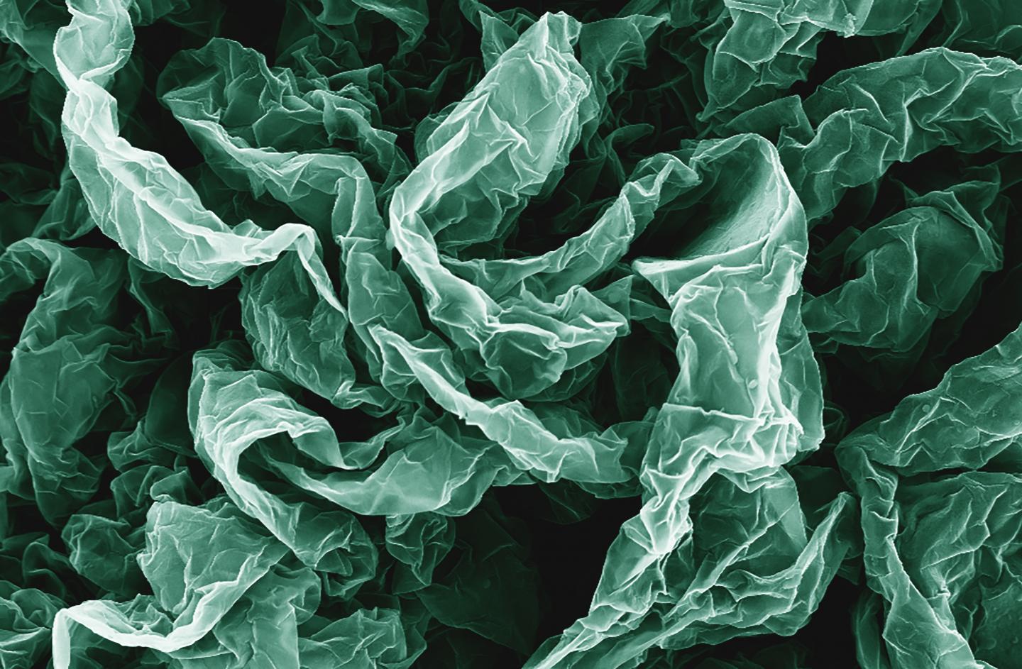
Caption: Wrinkles and crumples, introduced by placing graphene on shrinky polymers, can enhance graphene’s properties. Credit: Hurt and Wong Labs / Brown University
A March 21, 2016 news item on ScienceDaily describes how Brown University (US) researchers developed super-wrinkled and super-crumpled graphene,
Crumple a piece of paper and it’s probably destined for the trash can, but new research shows that repeatedly crumpling sheets of the nanomaterial graphene can actually enhance some of its properties. In some cases, the more crumpled the better.
The research by engineers from Brown University shows that graphene, wrinkled and crumpled in a multi-step process, becomes significantly better at repelling water–a property that could be useful in making self-cleaning surfaces. Crumpled graphene also has enhanced electrochemical properties, which could make it more useful as electrodes in batteries and fuel cells.
A March 21, 2016 Brown University news release (also on EurekAlert), which originated the news item, provides more detail about the current and previous research,
This new research builds on previous work done by Robert Hurt and Ian Wong, from Brown’s School of Engineering. The team had previously showed that by introducing wrinkles into graphene, they could make substrates for culturing cells that were more similar to the complex environments in which cells grow in the body. For this latest work, the researchers led by Po-Yen Chen, a Hibbit postdoctoral fellow, wanted to build more complex architectures incorporating both wrinkles and crumples. “I wanted to see if there was a way to create higher-generational structures,” Chen said.
To do that, the researchers deposited layers of graphene oxide onto shrink films–polymer membranes that shrink when heated (kids may know these as Shrinky Dinks [emphasis mine]). As the films shrink, the graphene on top is compressed, causing it to wrinkle and crumple. To see what kind of structures they could create, the researchers compressed same graphene sheets multiple times. After the first shrink, the film was dissolved away, and the graphene was placed in a new film to be shrunk again.
The researchers experimented with different configurations in the successive generations of shrinking. For example, sometimes they clamped opposite ends of the films, which caused them to shrink only along one axis. Clamped films yielded graphene sheets with periodic, basically parallel wrinkles across its surface. Unclamped films shrank in two dimensions, both length- and width-wise, creating a graphene surface that was crumpled in random shapes.
The team experimented with those different modes of shrinking over three successive generations. For example, they might shrink the same graphene sheet on a clamped film, then an unclamped film, then clamped again; or unclamped, clamped, unclamped. They also rotated the graphene in different configurations between shrinkings, sometimes placing the sheet perpendicular to its original orientation.
The team found that the multi-generational approach could substantially compress the graphene sheets, making them as small as one-fortieth their original size. They also showed that successive generations could create interesting patterns along the surface–wrinkles and crumples that were superimposed onto each other, for example.
“As you go deeper into the generations you tend to get larger wavelength structures with the original, smaller wavelength structure from earlier generations built into them,” said Robert Hurt, a professor of engineering at Brown and one of the paper’s corresponding authors.
A sheet that was shrunk clamped, unclamped, and then clamped looked different from ones that were unclamped, clamped, unclamped, for example.
“The sequence matters,” said Wong, also a corresponding author on the paper. “It’s not like multiplication where 2 times 3 is the same as 3 times 2. The material has a ‘memory’ and we get different results when we wrinkle or crumple in a different order.”
The researchers generated a kind of taxonomy of structures born from different shrinking configurations. They then tested several of those structures to see how they altered the properties of the graphene sheets.
Enhanced properties
They showed that a highly crumpled graphene surface becomes superhydrophobic–able to resist wetting by water. When water touches a hydrophobic surface, it beads up and rolls off. When the contact angle of those water beads with an underlying surface exceeds 160 degrees–meaning very little of the water bead’s surface touches the material–the material is said to be superhydrophobic. The researchers showed that they could make superhydrophobic graphene with three unclamped shrinks.
The team also showed that crumpling could enhance the electrochemical behaviors of graphene, which could be useful in next-generation energy storage and generation. The research showed that crumpled graphene used as a battery electrode had as much as a 400 percent increase in electrochemical current density over flat graphene sheets. That increase in current density could make for vastly more efficient batteries.
“You don’t need a new material to do it,” Chen said. “You just need to crumple the graphene.”
In additional to batteries and water resistant coatings, graphene compressed in this manner might also be useful in stretchable electronics–a wearable sensor, for example.
The group plans to continue experimenting with different ways of generating structures on graphene and other nanomaterials.
“There are many new two-dimensional nanomaterials that have interesting properties, not just graphene,” Wong said. “So other materials or combinations of materials may also organize into interesting structures with unexpected functionalities.”
Here’s a link to and a citation for the paper,
Multiscale Graphene Topographies Programmed by Sequential Mechanical Deformation by Po-Yen Chen, Jaskiranjeet Sodhi, Yang Qiu, Thomas M. Valentin, Ruben Spitz Steinberg, Zhongying Wang, Robert H. Hurt, and Ian Y. Wong. Advanced Materials DOI: 10.1002/adma.201506194 Article first published online: 21 MAR 2016
© 2016 WILEY-VCH Verlag GmbH & Co. KGaA, Weinheim
This paper is behind a paywall.
As for Shrinky Dinks, I first featured this material and its use in science research in an Aug. 16, 2010 posting about Shrinky Dinks and nanopatterning. It was originally developed by Betty J. Morris as craft material for children. Both she and the scientist kindly answered some followup questions inspired by the original news release and published in the 2010 post.