Tag Archives: CNRS

Human lung enzyme can degrade graphene

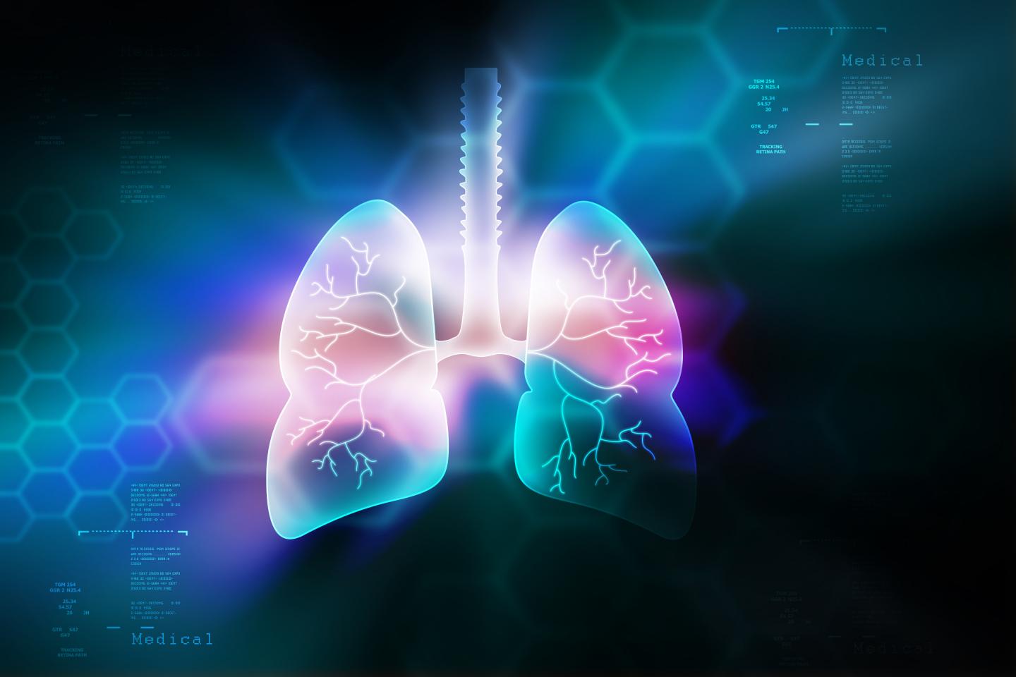
Caption: A human lung enzyme can biodegrade graphene. Credit: Fotolia Courtesy: Graphene Flagship

The big European Commission research programme, Grahene Flagship, has announced some new work with widespread implications if graphene is to be used in biomedical implants. From a August 23, 2018 news item on ScienceDaily,

Myeloperoxidase — an enzyme naturally found in our lungs — can biodegrade pristine graphene, according to the latest discovery of Graphene Flagship partners in CNRS, University of Strasbourg (France), Karolinska Institute (Sweden) and University of Castilla-La Mancha (Spain). Among other projects, the Graphene Flagship designs based like flexible biomedical electronic devices that will interfaced with the human body. Such applications require graphene to be biodegradable, so our body can be expelled from the body.

An August 23, 2018 Grapehene Flagship press release (mildly edited version on EurekAlert), which originated the news item, provides more detail,

To test how graphene behaves within the body, researchers analysed how it was broken down with the addition of a common human enzyme – myeloperoxidase or MPO. If a foreign body or bacteria is detected, neutrophils surround it and secrete MPO, thereby destroying the threat. Previous work by Graphene Flagship partners found that MPO could successfully biodegrade graphene oxide.

However, the structure of non-functionalized graphene was thought to be more resistant to degradation. To test this, the team looked at the effects of MPO ex vivo on two graphene forms; single- and few-layer.

Alberto Bianco, researcher at Graphene Flagship Partner CNRS, explains: “We used two forms of graphene, single- and few-layer, prepared by two different methods in water. They were then taken and put in contact with myeloperoxidase in the presence of hydrogen peroxide. This peroxidase was able to degrade and oxidise them. This was really unexpected, because we thought that non-functionalized graphene was more resistant than graphene oxide.”

Rajendra Kurapati, first author on the study and researcher at Graphene Flagship Partner CNRS, remarks how “the results emphasize that highly dispersible graphene could be degraded in the body by the action of neutrophils. This would open the new avenue for developing graphene-based materials.”

With successful ex-vivo testing, in-vivo testing is the next stage. Bengt Fadeel, professor at Graphene Flagship Partner Karolinska Institute believes that “understanding whether graphene is biodegradable or not is important for biomedical and other applications of this material. The fact that cells of the immune system are capable of handling graphene is very promising.”

Prof. Maurizio Prato, the Graphene Flagship leader for its Health and Environment Work Package said that “the enzymatic degradation of graphene is a very important topic, because in principle, graphene dispersed in the atmosphere could produce some harm. Instead, if there are microorganisms able to degrade graphene and related materials, the persistence of these materials in our environment will be strongly decreased. These types of studies are needed.” “What is also needed is to investigate the nature of degradation products,” adds Prato. “Once graphene is digested by enzymes, it could produce harmful derivatives. We need to know the structure of these derivatives and study their impact on health and environment,” he concludes.

Prof. Andrea C. Ferrari, Science and Technology Officer of the Graphene Flagship, and chair of its management panel added: “The report of a successful avenue for graphene biodegradation is a very important step forward to ensure the safe use of this material in applications. The Graphene Flagship has put the investigation of the health and environment effects of graphene at the centre of its programme since the start. These results strengthen our innovation and technology roadmap.”

Here’s a link to and a citation for the paper,

Degradation of Single‐Layer and Few‐Layer Graphene by Neutrophil Myeloperoxidase by Dr. Rajendra Kurapati, Dr. Sourav P. Mukherjee, Dr. Cristina Martín, Dr. George Bepete, Prof. Ester Vázquez, Dr. Alain Pénicaud, Prof. Dr. Bengt Fadeel, Dr. Alberto Bianco. Angewandte Chemie https://doi.org/10.1002/anie.201806906 First published: 13 July 2018

This paper is behind a paywall.

Nanocar Race winners: The US-Austrian team

Sadly, I didn’t stumble across the news about the US-Austrian team sooner but it was not published until a May 8, 2017 news item on Nanowerk,

Rice University chemist James Tour and his international team have won the first Nanocar Race.

The Rice and University of Graz team finished first in the inaugural Nanocar Race in Toulouse, France, April 28, completing a 150-nanometer course — roughly a thousandth of the width of a human hair — in about 1½ hours. (The race was declared over after 30 hours.)

Interestingly the Rice University news release announcing the win was issued prior to the ‘winning’ Swiss team’s and it explains why the Swiss team was declared a co-winner despite the additional hours (6.5 hours as compared to 1.5 hours [see my May 9, 2017 posting: Nanocar Race winners! where the Swiss appear to claiming they raced 38 hours]) before completing the race. From an April 28, 2017 Rice University news release,

The team led by Tour and Graz physicist Leonhard Grill deployed a two-wheeled, single-molecule vehicle with adamantane tires on its home track in Graz, Austria, achieving an average speed of 95 nanometers per hour. Tour said the speed ranged from more than 300 to less than 1 nanometer per hour, depending upon the location along the course.

The Swiss Nano Dragster team finished next, five hours later. But organizers at the French National Center for Scientific Research declared them a co-winner of first place as they were tops among teams that raced on a gold track.

Because the scanning tunneling microscope track in Toulouse could only accommodate four cars, two of the six competing international teams — Ohio University and Rice-Graz — ran their vehicles on their home tracks (Ohio on gold) and operated them remotely from the Toulouse headquarters.

The Dipolar Racer designed at Rice.

The Dipolar Racer designed at Rice.

Five cars were driven across gold surfaces in a vacuum near absolute zero by electrons from the tips of microscopes in Toulouse and Ohio, but the Rice-Graz team got permission to use a silver track at Graz. “Gold was the surface of choice, so we tested it there, but it turns out it’s too fast,” Grill said. “It’s so fast, we can’t even image it.”

The team got permission from organizers in advance of the race to use the slower silver surface, but with an additional handicap. “We had to go 150 nanometers around two pylons instead of 100 nanometers since our car was so much faster,” Tour said.

Tour said the race directors used the Paris-Rouen auto race in 1894, considered by some to be the world’s first auto race, as precedent for their decision April 29. “I am told there will be two first prizes regardless of the time difference and handicap,” he said.

The Rice-Graz car, called the Dipolar Racer, was designed by Tour and former Rice graduate student Victor Garcia-Lopez and raced by the Graz team, which included postdoctoral researcher and pilot Grant Simpson and undergraduate and co-pilot Philipp Petermeier.

The silver track under the microscope. Two Rice nanocars are in the blue circle at top. The lower car was the first to run the race, finishing in an hour-and-a-half. The top car was put through the course later, finishing in 2 hours.

The silver track under the microscope. Two Rice nanocars are in the blue circle at top. The lower car was the first to run the race, finishing in a 1½ hours. The top car was put through the course later, finishing in 2 hours. Click on the image for a larger version.

The purpose of the competition, according to organizers, was to push the science of how single molecules can be manipulated as they interact with surfaces.

“We chose our fastest wheels and our strongest dipole so that it could be pulled by the electric field more efficiently,” said Tour, whose lab has been designing nanocars since 1998. ‘We gave it two (side-by-side) wheels to minimize interaction with the surface and to lower the molecular weight.

“We built in every possible design parameter that we could to optimize speed,” he said.

While details of the Dipolar Racer remained a closely held secret until race time, Tour and Grill said they will be revealed in a forthcoming paper.

“This is the beginning of our ability to demonstrate nanoscale manipulation with control around obstacles and speed and will pave the way for much faster paces and eventually for carrying cargo and doing bottom-up assembly.

“It’s a great day for nanotechnology,” Tour said. “And a great day for Rice University and the University of Graz.”

Clearly all the winners were very excited. Still, there’s a little shade being thrown (one of the scientists is just a tiny bit miffed) as you can see in James Tour’s quote given after noting the US-Austrian racer was too fast for the gold surface so the team used the slower silver surface and were given another handicap. As per the Rice University news release: ““I am told [emphasis mine] there will be two first prizes regardless of the time difference and handicap,” he said.” Of course, the Swiss team’s news release didn’t mention the US-Austrian team’s speedier finish nor did it name (Dipolar Racer) the US-Austrian racer. As I noted before, scientists are people too.

Nanocar Race winners!

In fact, there was a tie although it seems the Swiss winners were a little more excited. A May 1, 2017 news item on swissinfo.ch provides fascinating detail,

“Swiss Nano Dragster”, driven by scientists from Basel, has won the first international car race involving molecular machines. The race involved four nano cars zipping round a pure gold racetrack measuring 100 nanometres – or one ten-thousandth of a millimetre.

The two Swiss pilots, Rémy Pawlak and Tobias Meier from the Swiss Nanoscience Institute and the Department of Physicsexternal link at the University of Basel, had to reach the chequered flag – negotiating two curves en route – within 38 hours. [emphasis mine*]

The winning drivers, who actually shared first place with a US-Austrian team, were not sitting behind a steering wheel but in front of a computer. They used this to propel their single-molecule vehicle with a small electric shock from a scanning tunnelling microscope.

During such a race, a tunnelling current flows between the tip of the microscope and the molecule, with the size of the current depending on the distance between molecule and tip. If the current is high enough, the molecule starts to move and can be steered over the racetrack, a bit like a hovercraft.

….

The race track was maintained at a very low temperature (-268 degrees Celsius) so that the molecules didn’t move without the current.

What’s more, any nudging of the molecule by the microscope tip would have led to disqualification.

Miniature motors

The race, held in Toulouse, France, and organised by the National Centre for Scientific Research (CNRS), was originally going to be held in October 2016, but problems with some cars resulted in a slight delay. In the end, organisers selected four of nine applicants since there were only four racetracks.

The cars measured between one and three nanometres – about 30,000 times smaller than a human hair. The Swiss Nano Dragster is, in technical language, a 4′-(4-Tolyl)-2,2′:6′,2”-terpyridine molecule.

The Swiss and US-Austrian teams outraced rivals from the US and Germany.

The race is not just a bit of fun for scientists. The researchers hope to gain insights into how molecules move.

I believe this Basel University .gif is from the race,

*Emphasis added on May 9, 2017 at 12:26 pm PT. See my May 9, 2017 posting: Nanocar Race winners: The US-Austrian team for the other half of this story.

Predicting how a memristor functions

An April 3, 2017 news item on Nanowerk announces a new memristor development (Note: A link has been removed),

Researchers from the CNRS [Centre national de la recherche scientifique; France] , Thales, and the Universities of Bordeaux, Paris-Sud, and Evry have created an artificial synapse capable of learning autonomously. They were also able to model the device, which is essential for developing more complex circuits. The research was published in Nature Communications (“Learning through ferroelectric domain dynamics in solid-state synapses”)

An April 3, 2017 CNRS press release, which originated the news item, provides a nice introduction to the memristor concept before providing a few more details about this latest work (Note: A link has been removed),

One of the goals of biomimetics is to take inspiration from the functioning of the brain [also known as neuromorphic engineering or neuromorphic computing] in order to design increasingly intelligent machines. This principle is already at work in information technology, in the form of the algorithms used for completing certain tasks, such as image recognition; this, for instance, is what Facebook uses to identify photos. However, the procedure consumes a lot of energy. Vincent Garcia (Unité mixte de physique CNRS/Thales) and his colleagues have just taken a step forward in this area by creating directly on a chip an artificial synapse that is capable of learning. They have also developed a physical model that explains this learning capacity. This discovery opens the way to creating a network of synapses and hence intelligent systems requiring less time and energy.

Our brain’s learning process is linked to our synapses, which serve as connections between our neurons. The more the synapse is stimulated, the more the connection is reinforced and learning improved. Researchers took inspiration from this mechanism to design an artificial synapse, called a memristor. This electronic nanocomponent consists of a thin ferroelectric layer sandwiched between two electrodes, and whose resistance can be tuned using voltage pulses similar to those in neurons. If the resistance is low the synaptic connection will be strong, and if the resistance is high the connection will be weak. This capacity to adapt its resistance enables the synapse to learn.

Although research focusing on these artificial synapses is central to the concerns of many laboratories, the functioning of these devices remained largely unknown. The researchers have succeeded, for the first time, in developing a physical model able to predict how they function. This understanding of the process will make it possible to create more complex systems, such as a series of artificial neurons interconnected by these memristors.

As part of the ULPEC H2020 European project, this discovery will be used for real-time shape recognition using an innovative camera1 : the pixels remain inactive, except when they see a change in the angle of vision. The data processing procedure will require less energy, and will take less time to detect the selected objects. The research involved teams from the CNRS/Thales physics joint research unit, the Laboratoire de l’intégration du matériau au système (CNRS/Université de Bordeaux/Bordeaux INP), the University of Arkansas (US), the Centre de nanosciences et nanotechnologies (CNRS/Université Paris-Sud), the Université d’Evry, and Thales.


Image synapse


© Sören Boyn / CNRS/Thales physics joint research unit.

Artist’s impression of the electronic synapse: the particles represent electrons circulating through oxide, by analogy with neurotransmitters in biological synapses. The flow of electrons depends on the oxide’s ferroelectric domain structure, which is controlled by electric voltage pulses.


Here’s a link to and a citation for the paper,

Learning through ferroelectric domain dynamics in solid-state synapses by Sören Boyn, Julie Grollier, Gwendal Lecerf, Bin Xu, Nicolas Locatelli, Stéphane Fusil, Stéphanie Girod, Cécile Carrétéro, Karin Garcia, Stéphane Xavier, Jean Tomas, Laurent Bellaiche, Manuel Bibes, Agnès Barthélémy, Sylvain Saïghi, & Vincent Garcia. Nature Communications 8, Article number: 14736 (2017) doi:10.1038/ncomms14736 Published online: 03 April 2017

This paper is open access.

Thales or Thales Group is a French company, from its Wikipedia entry (Note: Links have been removed),

Thales Group (French: [talɛs]) is a French multinational company that designs and builds electrical systems and provides services for the aerospace, defence, transportation and security markets. Its headquarters are in La Défense[2] (the business district of Paris), and its stock is listed on the Euronext Paris.

The company changed its name to Thales (from the Greek philosopher Thales,[3] pronounced [talɛs] reflecting its pronunciation in French) from Thomson-CSF in December 2000 shortly after the £1.3 billion acquisition of Racal Electronics plc, a UK defence electronics group. It is partially state-owned by the French government,[4] and has operations in more than 56 countries. It has 64,000 employees and generated €14.9 billion in revenues in 2016. The Group is ranked as the 475th largest company in the world by Fortune 500 Global.[5] It is also the 10th largest defence contractor in the world[6] and 55% of its total sales are military sales.[4]

The ULPEC (Ultra-Low Power Event-Based Camera) H2020 [Horizon 2020 funded) European project can be found here,

The long term goal of ULPEC is to develop advanced vision applications with ultra-low power requirements and ultra-low latency. The output of the ULPEC project is a demonstrator connecting a neuromorphic event-based camera to a high speed ultra-low power consumption asynchronous visual data processing system (Spiking Neural Network with memristive synapses). Although ULPEC device aims to reach TRL 4, it is a highly application-oriented project: prospective use cases will b…

Finally, for anyone curious about Thales, the philosopher (from his Wikipedia entry), Note: Links have been removed,

Thales of Miletus (/ˈθeɪliːz/; Greek: Θαλῆς (ὁ Μῑλήσιος), Thalēs; c. 624 – c. 546 BC) was a pre-Socratic Greek/Phoenician philosopher, mathematician and astronomer from Miletus in Asia Minor (present-day Milet in Turkey). He was one of the Seven Sages of Greece. Many, most notably Aristotle, regard him as the first philosopher in the Greek tradition,[1][2] and he is otherwise historically recognized as the first individual in Western civilization known to have entertained and engaged in scientific philosophy.[3][4]

Off to the Nanocar Race: April 28, 2017

The Nanocar Race (which at one point was the NanoCar Race) took place on April 28 -29, 2017 in Toulouse, France. Presumably the fall 2016 race did not take place (as I had reported in my May 26, 2016 posting). A March 23, 2017 news item on ScienceDaily gave the latest news about the race,

Nanocars will compete for the first time ever during an international molecule-car race on April 28-29, 2017 in Toulouse (south-western France). The vehicles, which consist of a few hundred atoms, will be powered by minute electrical pulses during the 36 hours of the race, in which they must navigate a racecourse made of gold atoms, and measuring a maximum of a 100 nanometers in length. They will square off beneath the four tips of a unique microscope located at the CNRS’s Centre d’élaboration de matériaux et d’études structurales (CEMES) in Toulouse. The race, which was organized by the CNRS, is first and foremost a scientific and technological challenge, and will be broadcast live on the YouTube Nanocar Race channel. Beyond the competition, the overarching objective is to advance research in the observation and control of molecule-machines.

More than just a competition, the Nanocar Race is an international scientific experiment that will be conducted in real time, with the aim of testing the performance of molecule-machines and the scientific instruments used to control them. The years ahead will probably see the use of such molecular machinery — activated individually or in synchronized fashion — in the manufacture of common machines: atom-by-atom construction of electronic circuits, atom-by-atom deconstruction of industrial waste, capture of energy…The Nanocar Race is therefore a unique opportunity for researchers to implement cutting-edge techniques for the simultaneous observation and independent maneuvering of such nano-machines.

The experiment began in 2013 as part of an overview of nano-machine research for a scientific journal, when the idea for a car race took shape in the minds of CNRS senior researcher Christian Joachim (now the director of the race) and Gwénaël Rapenne, a Professor of chemistry at Université Toulouse III — Paul Sabatier. …

An April 19, 2017 article by Davide Castelvecchi for Nature (magazine) provided more detail about the race (Note: Links have been removed),

The term nanocar is actually a misnomer, because the molecules involved in this race have no motors. (Future races may incorporate them, Joachim says.) And it is not clear whether the molecules will even roll along like wagons: a few designs might, but many lack axles and wheels. Drivers will use electrons from the tip of a scanning tunnelling microscope (STM) to help jolt their molecules along, typically by just 0.3 nano-metres each time — making 100 nanometres “a pretty long distance”, notes physicist Leonhard Grill of the University of Graz, Austria, who co-leads a US–Austrian team in the race.

Contestants are not allowed to directly push on their molecules with the STM tip. Some teams have designed their molecules so that the incoming electrons raise their energy states, causing vibrations or changes to molecular structures that jolt the racers along. Others expect electrostatic repulsion from the electrons to be the main driving force. Waka Nakanishi, an organic chemist at the National Institute for Materials Science in Tsukuba, Japan, has designed a nanocar with two sets of ‘flaps’ that are intended to flutter like butterfly wings when the molecule is energized by the STM tip (see ‘Molecular race’). Part of the reason for entering the race, she says, was to gain access to the Toulouse lab’s state-of-the-art STM to better understand the molecule’s behaviour.

Eric Masson, a chemist at Ohio University in Athens, hopes to find out whether the ‘wheels’ (pumpkin-shaped groups of atoms) of his team’s car will roll on the surface or simply slide. “We want to better understand the nature of the interaction between the molecule and the surface,” says Masson..

Adapted from www.nanocar-race.cnrs.fr

Simply watching the race progress is half the battle. After each attempted jolt, teams will take three minutes to scan their race track with the STM, and after each hour they will produce a short animation that will immediately be posted online. That way, says Joachim, everyone will be able to see the race streamed almost live.

Nanoscale races

The Toulouse laboratory has an unusual STM with four scanning tips — most have only one — that will allow four teams to race at the same time, each on a different section of the gold surface. Six teams will compete this week to qualify for one of the four spots; the final race will begin on 28 April at 11 a.m. local time. The competitors will face many obstacles during the contest. Individual molecules in the race will often be lost or get stuck, and the trickiest part may be to negotiate the two turns in the track, Joachim says. He thinks the racers may require multiple restarts to cover the distance.

For anyone who wants more information, go to the Nanocar Race website. There is also a highlights video,

Published on Apr 29, 2017

The best moments of the first-ever international race of molecule- cars.

Graphene Canada and its second annual conference

An Aug. 31, 2016 news item on Nanotechnology Now announces Canada’s second graphene-themed conference,

The 2nd edition of Graphene & 2D Materials Canada 2016 International Conference & Exhibition (www.graphenecanadaconf.com) will take place in Montreal (Canada): 18-20 October, 2016.

– An industrial forum with focus on Graphene Commercialization (Abalonyx, Alcereco Inc, AMO GmbH, Avanzare, AzTrong Inc, Bosch GmbH, China Innovation Alliance of the Graphene Industry (CGIA), Durham University & Applied Graphene Materials, Fujitsu Laboratories Ltd., Hanwha Techwin, Haydale, IDTechEx, North Carolina Central University & Chaowei Power Ltd, NTNU&CrayoNano, Phantoms Foundation, Southeast University, The Graphene Council, University of Siegen, University of Sunderland and University of Waterloo)
– Extensive thematic workshops in parallel (Materials & Devices Characterization, Chemistry, Biosensors & Energy and Electronic Devices)
– A significant exhibition (Abalonyx, Go Foundation, Grafoid, Group NanoXplore Inc., Raymor | Nanointegris and Suragus GmbH)

As I noted in my 2015 post about Graphene Canada and its conference, the group is organized in a rather interesting fashion and I see the tradition continues, i.e., the lead organizers seem to be situated in countries other than Canada. From the Aug. 31, 2016 news item on Nanotechnology Now,

Organisers: Phantoms Foundation [located in Spain] www.phantomsnet.net
Catalan Institute of Nanoscience and Nanotechnology – ICN2 (Spain) | CEMES/CNRS (France) | GO Foundation (Canada) | Grafoid Inc (Canada) | Graphene Labs – IIT (Italy) | McGill University (Canada) | Texas Instruments (USA) | Université Catholique de Louvain (Belgium) | Université de Montreal (Canada)

You can find the conference website here.

Improving the quality of sight in artificial retinas

Researchers at France’s Centre national de la recherche scientifique (CNRS) and elsewhere have taken a step forward to improving sight derived from artificial retinas according to an Aug. 25, 2016 news item on Nanowerk (Note: A link has been removed),

A major therapeutic challenge, the retinal prostheses that have been under development during the past ten years can enable some blind subjects to perceive light signals, but the image thus restored is still far from being clear. By comparing in rodents the activity of the visual cortex generated artificially by implants against that produced by “natural sight”, scientists from CNRS, CEA [Commissariat à l’énergie atomique et aux énergies alternatives is the French Alternative Energies and Atomic Energy Commission], INSERM [Institut national de la santé et de la recherche médicale is the French National Institute of Health and Medical Research], AP-HM [Assistance Publique – Hôpitaux de Marseille] and Aix-Marseille Université identified two factors that limit the resolution of prostheses.

Based on these findings, they were able to improve the precision of prosthetic activation. These multidisciplinary efforts, published on 23 August 2016 in eLife (“Probing the functional impact of sub-retinal prosthesis”), thus open the way towards further advances in retinal prostheses that will enhance the quality of life of implanted patients.

An Aug. 24, 2015 CNRS press release, which originated the news item, expands on the theme,

A retinal prosthesis comprises three elements: a camera (inserted in the patient’s spectacles), an electronic microcircuit (which transforms data from the camera into an electrical signal) and a matrix of microscopic electrodes (implanted in the eye in contact with the retina). This prosthesis replaces the photoreceptor cells of the retina: like them, it converts visual information into electrical signals which are then transmitted to the brain via the optic nerve. It can treat blindness caused by a degeneration of retinal photoreceptors, on condition that the optical nerve has remained functional1. Equipped with these implants, patients who were totally blind can recover visual perceptions in the form of light spots, or phosphenes.  Unfortunately, at present, the light signals perceived are not clear enough to recognize faces, read or move about independently.

To understand the resolution limits of the image generated by the prosthesis, and to find ways of optimizing the system, the scientists carried out a large-scale experiment on rodents.  By combining their skills in ophthalmology and the physiology of vision, they compared the response of the visual system of rodents to both natural visual stimuli and those generated by the prosthesis.

Their work showed that the prosthesis activated the visual cortex of the rodent in the correct position and at ranges comparable to those obtained under natural conditions.  However, the extent of the activation was much too great, and its shape was much too elongated.  This deformation was due to two separate phenomena observed at the level of the electrode matrix. Firstly, the scientists observed excessive electrical diffusion: the thin layer of liquid situated between the electrode and the retina passively diffused the electrical stimulus to neighboring nerve cells. And secondly, they detected the unwanted activation of retinal fibers situated close to the cells targeted for stimulation.

Armed with these findings, the scientists were able to improve the properties of the interface between the prosthesis and retina, with the help of specialists in interface physics.  Together, they were able to generate less diffuse currents and significantly improve artificial activation, and hence the performance of the prosthesis.

This lengthy study, because of the range of parameters covered (to study the different positions, types and intensities of signals) and the surgical problems encountered (in inserting the implant and recording the images generated in the animal’s brain) has nevertheless opened the way towards making promising improvements to retinal prostheses for humans.

This work was carried out by scientists from the Institut de Neurosciences de la Timone (CNRS/AMU) and AP-HM, in collaboration with CEA-Leti and the Institut de la Vision (CNRS/Inserm/UPMC).

Artificial retinas


© F. Chavane & S. Roux.

Activation (colored circles at the level of the visual cortex) of the visual system by prosthetic stimulation (in the middle, in red, the insert shows an image of an implanted prosthesis) is greater and more elongated than the activation achieved under natural stimulation (on the left, in yellow). Using a protocol to adapt stimulation (on the right, in green), the size and shape of the activation can be controlled and are more similar to natural visual activation (yellow).


Here’s a link to and a citation for the paper,

Probing the functional impact of sub-retinal prosthesis by Sébastien Roux, Frédéric Matonti, Florent Dupont, Louis Hoffart, Sylvain Takerkart, Serge Picaud, Pascale Pham, and Frédéric Chavane. eLife 2016;5:e12687 DOI: http://dx.doi.org/10.7554/eLife.12687 Published August 23, 2016

This paper appears to be open access.

New electrochromic material for ‘smart’ windows

Given that it’s summer, I seem to be increasingly obsessed with windows that help control the heat from the sun. So, this Aug. 22, 2016 news item on ScienceDaily hit my sweet spot,

Researchers in the Cockrell School of Engineering at The University of Texas at Austin have invented a new flexible smart window material that, when incorporated into windows, sunroofs, or even curved glass surfaces, will have the ability to control both heat and light from the sun. …

Delia Milliron, an associate professor in the McKetta Department of Chemical Engineering, and her team’s advancement is a new low-temperature process for coating the new smart material on plastic, which makes it easier and cheaper to apply than conventional coatings made directly on the glass itself. The team demonstrated a flexible electrochromic device, which means a small electric charge (about 4 volts) can lighten or darken the material and control the transmission of heat-producing, near-infrared radiation. Such smart windows are aimed at saving on cooling and heating bills for homes and businesses.

An Aug. 22, 2016 University of Texas at Austin news release (also on EurekAlert), which originated the news item, describes the international team behind this research and offers more details about the research itself,

The research team is an international collaboration, including scientists at the European Synchrotron Radiation Facility and CNRS in France, and Ikerbasque in Spain. Researchers at UT Austin’s College of Natural Sciences provided key theoretical work.

Milliron and her team’s low-temperature process generates a material with a unique nanostructure, which doubles the efficiency of the coloration process compared with a coating produced by a conventional high-temperature process. It can switch between clear and tinted more quickly, using less power.

The new electrochromic material, like its high-temperature processed counterpart, has an amorphous structure, meaning the atoms lack any long-range organization as would be found in a crystal. However, the new process yields a unique local arrangement of the atoms in a linear, chain-like structure. Whereas conventional amorphous materials produced at high temperature have a denser three-dimensionally bonded structure, the researchers’ new linearly structured material, made of chemically condensed niobium oxide, allows ions to flow in and out more freely. As a result, it is twice as energy efficient as the conventionally processed smart window material.

At the heart of the team’s study is their rare insight into the atomic-scale structure of the amorphous materials, whose disordered structures are difficult to characterize. Because there are few techniques for characterizing the atomic-scale structure sufficiently enough to understand properties, it has been difficult to engineer amorphous materials to enhance their performance.

“There’s relatively little insight into amorphous materials and how their properties are impacted by local structure,” Milliron said. “But, we were able to characterize with enough specificity what the local arrangement of the atoms is, so that it sheds light on the differences in properties in a rational way.”

Graeme Henkelman, a co-author on the paper and chemistry professor in UT Austin’s College of Natural Sciences, explains that determining the atomic structure for amorphous materials is far more difficult than for crystalline materials, which have an ordered structure. In this case, the researchers were able to use a combination of techniques and measurements to determine an atomic structure that is consistent in both experiment and theory.

“Such collaborative efforts that combine complementary techniques are, in my view, the key to the rational design of new materials,” Henkelman said.

Milliron believes the knowledge gained here could inspire deliberate engineering of amorphous materials for other applications such as supercapacitors that store and release electrical energy rapidly and efficiently.

The Milliron lab’s next challenge is to develop a flexible material using their low-temperature process that meets or exceeds the best performance of electrochromic materials made by conventional high-temperature processing.

“We want to see if we can marry the best performance with this new low-temperature processing strategy,” she said.

Here’s a link to and a citation for the paper,

Linear topology in amorphous metal oxide electrochromic networks obtained via low-temperature solution processing by Anna Llordés, Yang Wang, Alejandro Fernandez-Martinez, Penghao Xiao, Tom Lee, Agnieszka Poulain, Omid Zandi, Camila A. Saez Cabezas, Graeme Henkelman, & Delia J. Milliron. Nature Materials (2016)  doi:10.1038/nmat4734 Published online 22 August 2016

This paper is behind a paywall.

Promising new technique for controlled fabrication of nanowires

This research is the result of a collaboration between French, Italian, Australian, and Canadian researchers. From a Jan. 5, 2016 news item on *phys.org,

An international team of researchers including Professor Federico Rosei and members of his group at INRS (Institut national de la recherche scientifique) has developed a new strategy for fabricating atomically controlled carbon nanostructures used in molecular carbon-based electronics. An article just published in the prestigious journal Nature Communications presents their findings: the complete electronic structure of a conjugated organic polymer, and the influence of the substrate on its electronic properties.

A Jan. 5, 2016 INRS news release by Gisèle Bolduc, which originated the news item, indicates this is the beginning rather than an endpoint (Note: A link has been removed),

The researchers combined two procedures previously developed in Professor Rosei’s lab—molecular self-assembly and chain polymerization—to produce a network of long-range poly(para-phenylene) (PPP) nanowires on a copper (Cu) surface. Using advanced technologies such as scanning tunneling microscopy and photoelectron spectroscopy as well as theoretical models, they were able to describe the morphology and electronic structure of these nanostructures.

“We provide a complete description of the band structure and also highlight the strong interaction between the polymer and the substrate, which explains both the decreased bandgap and the metallic nature of the new chains. Even with this hybridization, the PPP bands display a quasi one-dimensional dispersion in conductive polymeric nanowires,” said Professor Federico Rosei, one of the authors of the study.

Although further research is needed to fully describe the electronic properties of these nanostructures, the polymer’s dispersion provides a spectroscopic record of the polymerization process of certain types of molecules on gold, silver, copper, and other surfaces. It’s a promising approach for similar semiconductor studies—an essential step in the development of actual devices.

The results of the study could be used in designing organic nanostructures, with significant potential applications in nanoelectronics, including photovoltaic devices, field-effect transistors, light-emitting diodes, and sensors.

About the article

This study was designed by Yannick Fagot-Revurat and Daniel Malterre of Université de Lorraine/CNRS, Federico Rosei of INRS, Josh Lipton-Duffin of the Institute for Future Environments (Australia), Giorgio Contini of the Italian National Research Council, and Dmytro F. Perepichka of McGill University. […]The researchers were generously supported by Conseil Franco-Québécois de coopération universitaire, the France–Italy International Program for Scientific Cooperation, the Natural Sciences and Engineering Research Council of Canada, Fonds québécois de recherche – Nature et technologies, and a Québec MEIE grant (in collaboration with Belgium).

Here’s a link to and a citation for the paper,

Quasi one-dimensional band dispersion and surface metallization in long-range ordered polymeric wires by Guillaume Vasseur, Yannick Fagot-Revurat, Muriel Sicot, Bertrand Kierren, Luc Moreau, Daniel Malterre, Luis Cardenas, Gianluca Galeotti, Josh Lipton-Duffin, Federico Rosei, Marco Di Giovannantonio, Giorgio Contini, Patrick Le Fèvre, François Bertran, Liangbo Liang, Vincent Meunier, Dmitrii F. Perepichka. Nature Communications 7, Article number:  10235 doi:10.1038/ncomms10235 Published 04 January 2016

This is an open access paper.

*’ScienceDaily’ corrected to ‘phys.org’ on Tues., Jan. 5, 2016 at 1615 PST.

Canada and some graphene scene tidbits

For a long time It seemed as if every country in the world, except Canada, had some some sort of graphene event. According to a July 16, 2015 news item on Nanotechnology Now, Canada has now stepped up, albeit, in a peculiarly Canadian fashion. First the news,

Mid October [Oct. 14 -16, 2015], the Graphene & 2D Materials Canada 2015 International Conference & Exhibition (www.graphenecanada2015.com) will take place in Montreal (Canada).

I found a July 16, 2015 news release (PDF) announcing the Canadian event on the lead organizer’s (Phantoms Foundation located in Spain) website,

On the second day of the event (15th October, 2015), an Industrial Forum will bring together top industry leaders to discuss recent advances in technology developments and business opportunities in graphene commercialization.
At this stage, the event unveils 38 keynote & invited speakers. On the Industrial Forum 19 of them will present the latest in terms of Energy, Applications, Production and Worldwide Initiatives & Priorities.

Plenary:
Gary Economo (Grafoid Inc., Canada)
Khasha Ghaffarzadeh (IDTechEx, UK)
Shu-Jen Han (IBM T.J. Watson Research Center, USA)
Bor Z. Jang (Angstron Materials, USA)
Seongjun Park (Samsung Advanced Institute of Technology (SAIT), Korea)
Chun-Yun Sung (Lockheed Martin, USA)

Parallel Sessions:
Gordon Chiu (Grafoid Inc., Canada)
Jesus de la Fuente (Graphenea, Spain)
Mark Gallerneault (ALCERECO Inc., Canada)
Ray Gibbs (Haydale Graphene Industries, UK)
Masataka Hasegawa (AIST, Japan)
Byung Hee Hong (SNU & Graphene Square, Korea)
Tony Ling (Jestico + Whiles, UK)
Carla Miner (SDTC, Canada)
Gregory Pognon (THALES Research & Technology, France)
Elena Polyakova (Graphene Laboratories Inc, USA)
Federico Rosei (INRS–EMT, Université du Québec, Canada)
Aiping Yu (University of Waterloo, Canada)
Hua Zhang (MSE-NTU, Singapore)

Apart from the industrial forum, several industry-related activities will be organized:
– Extensive thematic workshops in parallel (Standardization, Materials & Devices Characterization, Bio & Health and Electronic Devices)
– An exhibition carried out with the latest graphene trends (Grafoid, RAYMOR NanoIntegris, Nanomagnetics Instruments, ICEX and Xerox Research Centre of Canada (XRCC) already confirmed)
– B2B meetings to foster technical cooperation in the field of Graphene

It’s still possible to contribute to the event with an oral presentation. The call for abstracts is open until July, 20 [2015]. [emphasis mine]

Graphene Canada 2015 is already supported by Canada’s leading graphene applications developer, Grafoid Inc., Tourisme Montréal and Université de Montréal.

This is what makes the event peculiarly Canadian: multiculturalism, anyone? From the news release,

Organisers: Phantoms Foundation www.phantomsnet.net & Grafoid Foundation (lead organizers)

CEMES/CNRS (France) | Grafoid (Canada) | Catalan Institute of Nanoscience and Nanotechnology – ICN2 (Spain) | IIT (Italy) | McGill University, Canada | Texas Instruments (USA) | Université Catholique de Louvain (Belgium) | Université de Montreal, Canada

It’s billed as a ‘Canada Graphene 2015’ and, as I recall, these types of events don’t usually have so many other countries listed as organizers. For example, UK Graphene 2015 would have mostly or all of its organizers (especially the leads) located in the UK.

Getting to the Canadian content, I wrote about Grafoid at length tracking some of its relationships to companies it owns, a business deal with Hydro Québec, and a partnership with the University of Waterloo, and a nonrepayable grant from the Canadian federal government (Sustainable Development Technology Canada [SDTC]) in a Feb. 23, 2015 posting. Do take a look at the post if you’re curious about the heavily interlinked nature of the Canadian graphene scene and take another look at the list of speakers and their agencies (Mark Gallerneault of ALCERECO [partially owned by Grafoid], Carla Miner of SDTC [Grafoid received monies from the Canadian federal department],  Federico Rosei of INRS–EMT, Université du Québec [another Quebec link], Aiping Yu, University of Waterloo [an academic partner to Grafoid]). The Canadian graphene community is a small one so it’s not surprising there are links between the Canadian speakers but it does seem odd that Lomiko Metals is not represented here. Still, new speakers have been announced since the news release (e.g., Frank Koppens of ICFO, Spain, and Vladimir Falko of Lancaster University, UK) so  time remains.

Meanwhile, Lomiko Metals has announced in a July 17, 2015 news item on Azonano that Graphene 3D labs has changed the percentage of its outstanding shares affecting the percentage that Lomiko owns, amid some production and distribution announcements. The bit about launching commercial sales of its graphene filament seems more interesting to me,

On March 16, 2015 Graphene 3D Lab (TSXV:GGG) (OTCQB:GPHBF) announced that it launched commercial sales of its Conductive Graphene Filament for 3D printing. The filament incorporates highly conductive proprietary nano-carbon materials to enhance the properties of PLA, a widely used thermoplastic material for 3D printing; therefore, the filament is compatible with most commercially available 3D printers. The conductive filament can be used to print conductive traces (similar to as used in circuit boards) within 3D printed parts for electronics.

So, that’s all I’ve got for Canada’s graphene scene.