Tag Archives: Hao Jiang

Combining silicon with metal oxide memristors to create powerful, low-energy intensive chips enabling AI in portable devices

In this one week, I’m publishing my first stories (see also June 13, 2023 posting “ChatGPT and a neuromorphic [brainlike] synapse“) where artificial intelligence (AI) software is combined with a memristor (hardware component) for brainlike (neuromorphic) computing.

Here’s more about some of the latest research from a March 30, 2023 news item on ScienceDaily,

Everyone is talking about the newest AI and the power of neural networks, forgetting that software is limited by the hardware on which it runs. But it is hardware, says USC [University of Southern California] Professor of Electrical and Computer Engineering Joshua Yang, that has become “the bottleneck.” Now, Yang’s new research with collaborators might change that. They believe that they have developed a new type of chip with the best memory of any chip thus far for edge AI (AI in portable devices).

A March 29, 2023 University of Southern California (USC) news release (also on EurekAlert), which originated the news item, contextualizes the research and delves further into the topic of neuromorphic hardware,

For approximately the past 30 years, while the size of the neural networks needed for AI and data science applications doubled every 3.5 months, the hardware capability needed to process them doubled only every 3.5 years. According to Yang, hardware presents a more and more severe problem for which few have patience. 

Governments, industry, and academia are trying to address this hardware challenge worldwide. Some continue to work on hardware solutions with silicon chips, while others are experimenting with new types of materials and devices.  Yang’s work falls into the middle—focusing on exploiting and combining the advantages of the new materials and traditional silicon technology that could support heavy AI and data science computation. 

Their new paper in Nature focuses on the understanding of fundamental physics that leads to a drastic increase in memory capacity needed for AI hardware. The team led by Yang, with researchers from USC (including Han Wang’s group), MIT [Massachusetts Institute of Technology], and the University of Massachusetts, developed a protocol for devices to reduce “noise” and demonstrated the practicality of using this protocol in integrated chips. This demonstration was made at TetraMem, a startup company co-founded by Yang and his co-authors  (Miao Hu, Qiangfei Xia, and Glenn Ge), to commercialize AI acceleration technology. According to Yang, this new memory chip has the highest information density per device (11 bits) among all types of known memory technologies thus far. Such small but powerful devices could play a critical role in bringing incredible power to the devices in our pockets. The chips are not just for memory but also for the processor. And millions of them in a small chip, working in parallel to rapidly run your AI tasks, could only require a small battery to power it. 

The chips that Yang and his colleagues are creating combine silicon with metal oxide memristors in order to create powerful but low-energy intensive chips. The technique focuses on using the positions of atoms to represent information rather than the number of electrons (which is the current technique involved in computations on chips). The positions of the atoms offer a compact and stable way to store more information in an analog, instead of digital fashion. Moreover, the information can be processed where it is stored instead of being sent to one of the few dedicated ‘processors,’ eliminating the so-called ‘von Neumann bottleneck’ existing in current computing systems.  In this way, says Yang, computing for AI is “more energy efficient with a higher throughput.”

How it works: 

Yang explains that electrons which are manipulated in traditional chips, are “light.” And this lightness, makes them prone to moving around and being more volatile.  Instead of storing memory through electrons, Yang and collaborators are storing memory in full atoms. Here is why this memory matters. Normally, says Yang, when one turns off a computer, the information memory is gone—but if you need that memory to run a new computation and your computer needs the information all over again, you have lost both time and energy.  This new method, focusing on activating atoms rather than electrons, does not require battery power to maintain stored information. Similar scenarios happen in AI computations, where a stable memory capable of high information density is crucial. Yang imagines this new tech that may enable powerful AI capability in edge devices, such as Google Glasses, which he says previously suffered from a frequent recharging issue.

Further, by converting chips to rely on atoms as opposed to electrons, chips become smaller.  Yang adds that with this new method, there is more computing capacity at a smaller scale. And this method, he says, could offer “many more levels of memory to help increase information density.” 

To put it in context, right now, ChatGPT is running on a cloud. The new innovation, followed by some further development, could put the power of a mini version of ChatGPT in everyone’s personal device. It could make such high-powered tech more affordable and accessible for all sorts of applications. 

Here’s a link to and a citation for the paper,

Thousands of conductance levels in memristors integrated on CMOS by Mingyi Rao, Hao Tang, Jiangbin Wu, Wenhao Song, Max Zhang, Wenbo Yin, Ye Zhuo, Fatemeh Kiani, Benjamin Chen, Xiangqi Jiang, Hefei Liu, Hung-Yu Chen, Rivu Midya, Fan Ye, Hao Jiang, Zhongrui Wang, Mingche Wu, Miao Hu, Han Wang, Qiangfei Xia, Ning Ge, Ju Li & J. Joshua Yang. Nature volume 615, pages 823–829 (2023) DOI: https://doi.org/10.1038/s41586-023-05759-5 Issue Date: 30 March 2023 Published: 29 March 2023

This paper is behind a paywall.
A new memristor circuit

Apparently engineers at the University of Massachusetts at Amherst have developed a new kind of memristor. A Sept. 29, 2016 news item on Nanowerk makes the announcement (Note: A link has been removed),

Engineers at the University of Massachusetts Amherst are leading a research team that is developing a new type of nanodevice for computer microprocessors that can mimic the functioning of a biological synapse—the place where a signal passes from one nerve cell to another in the body. The work is featured in the advance online publication of Nature Materials (“Memristors with diffusive dynamics as synaptic emulators for neuromorphic computing”).

Such neuromorphic computing in which microprocessors are configured more like human brains is one of the most promising transformative computing technologies currently under study.

While it doesn’t sound different from any other memristor, that’s misleading. Do read on. A Sept. 27, 2016 University of Massachusetts at Amherst news release, which originated the news item, provides more detail about the researchers and the work,

J. Joshua Yang and Qiangfei Xia are professors in the electrical and computer engineering department in the UMass Amherst College of Engineering. Yang describes the research as part of collaborative work on a new type of memristive device.

Memristive devices are electrical resistance switches that can alter their resistance based on the history of applied voltage and current. These devices can store and process information and offer several key performance characteristics that exceed conventional integrated circuit technology.

“Memristors have become a leading candidate to enable neuromorphic computing by reproducing the functions in biological synapses and neurons in a neural network system, while providing advantages in energy and size,” the researchers say.

Neuromorphic computing—meaning microprocessors configured more like human brains than like traditional computer chips—is one of the most promising transformative computing technologies currently under intensive study. Xia says, “This work opens a new avenue of neuromorphic computing hardware based on memristors.”

They say that most previous work in this field with memristors has not implemented diffusive dynamics without using large standard technology found in integrated circuits commonly used in microprocessors, microcontrollers, static random access memory and other digital logic circuits.

The researchers say they proposed and demonstrated a bio-inspired solution to the diffusive dynamics that is fundamentally different from the standard technology for integrated circuits while sharing great similarities with synapses. They say, “Specifically, we developed a diffusive-type memristor where diffusion of atoms offers a similar dynamics [?] and the needed time-scales as its bio-counterpart, leading to a more faithful emulation of actual synapses, i.e., a true synaptic emulator.”

The researchers say, “The results here provide an encouraging pathway toward synaptic emulation using diffusive memristors for neuromorphic computing.”

Here’s a link to and a citation for the paper,

Memristors with diffusive dynamics as synaptic emulators for neuromorphic computing by Zhongrui Wang, Saumil Joshi, Sergey E. Savel’ev, Hao Jiang, Rivu Midya, Peng Lin, Miao Hu, Ning Ge, John Paul Strachan, Zhiyong Li, Qing Wu, Mark Barnell, Geng-Lin Li, Huolin L. Xin, R. Stanley Williams [emphasis mine], Qiangfei Xia, & J. Joshua Yang. Nature Materials (2016) doi:10.1038/nmat4756 Published online 26 September 2016

This paper is behind a paywall.

I’ve emphasized R. Stanley Williams’ name as he was the lead researcher on the HP Labs team that proved Leon Chua’s 1971 theory about the memristor and exerted engineering control of the memristor in 2008. (Bernard Widrow, in the 1960s,  predicted and proved the existence of something he termed a ‘memistor’. Chua arrived at his ‘memristor’ theory independently.)

Austin Silver in a Sept. 29, 2016 posting on The Human OS blog (on the IEEE [Institute of Electrical and Electronics Engineers] website) delves into this latest memristor research (Note: Links have been removed),

In research published in Nature Materials on 26 September [2016], Yang and his team mimicked a crucial underlying component of how synaptic connections get stronger or weaker: the flow of calcium.

The movement of calcium into or out of the neuronal membrane, neuroscientists have found, directly affects the connection. Chemical processes move the calcium in and out— triggering a long-term change in the synapses’ strength. 2015 research in ACS NanoLetters and Advanced Functional Materials discovered that types of memristors can simulate some of the calcium behavior, but not all.

In the new research, Yang combined two types of memristors in series to create an artificial synapse. The hybrid device more closely mimics biological synapse behavior—the calcium flow in particular, Yang says.

The new memristor used–called a diffusive memristor because atoms in the resistive material move even without an applied voltage when the device is in the high resistance state—was a dielectic film sandwiched between Pt [platinum] or Au [gold] electrodes. The film contained Ag [silver] nanoparticles, which would play the role of calcium in the experiments.

By tracking the movement of the silver nanoparticles inside the diffusive memristor, the researchers noticed a striking similarity to how calcium functions in biological systems.

A voltage pulse to the hybrid device drove silver into the gap between the diffusive memristor’s two electrodes–creating a filament bridge. After the pulse died away, the filament started to break and the silver moved back— resistance increased.

Like the case with calcium, a force made silver go in and a force made silver go out.

To complete the artificial synapse, the researchers connected the diffusive memristor in series to another type of memristor that had been studied before.

When presented with a sequence of voltage pulses with particular timing, the artificial synapse showed the kind of long-term strengthening behavior a real synapse would, according to the researchers. “We think it is sort of a real emulation, rather than simulation because they have the physical similarity,” Yang says.

I was glad to find some additional technical detail about this new memristor and to find the Human OS blog, which is new to me and according to its home page is a “biomedical blog, featuring the wearable sensors, big data analytics, and implanted devices that enable new ventures in personalized medicine.”

Wood chip/computer chip, a cellulose nanofibril development

I imagine researchers at the University of Wisconsin-Madison and the US Department of Agriculture Forest Products Laboratory (FPL) are hoping they have managed to create a wood-based computer chip that can be commercialized in the near future. From a May 26, 2015 news item on ScienceDaily,

Portable electronics — typically made of non-renewable, non-biodegradable and potentially toxic materials — are discarded at an alarming rate in consumers’ pursuit of the next best electronic gadget.

In an effort to alleviate the environmental burden of electronic devices, a team of University of Wisconsin-Madison researchers has collaborated with researchers in the Madison-based U.S. Department of Agriculture Forest Products Laboratory (FPL) to develop a surprising solution: a semiconductor chip made almost entirely of wood.

The research team, led by UW-Madison electrical and computer engineering professor Zhenqiang “Jack” Ma, described the new device in a paper published today (May 26, 2015) by the journal Nature Communications. The paper demonstrates the feasibility of replacing the substrate, or support layer, of a computer chip, with cellulose nanofibril (CNF), a flexible, biodegradable material made from wood.

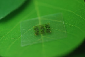
Here’s what the wood computer chip looks like,

A cellulose nanofibril (CNF) computer chip rests on a leaf. Photo: Yei Hwan Jung, Wisconsin Nano Engineering Device Laboratory

A cellulose nanofibril (CNF) computer chip rests on a leaf. Photo: Yei Hwan Jung, Wisconsin Nano Engineering Device Laboratory Courtesy University of Wisconsin-Madison

A May 25, 2015 University of Wisconsin-Madison news release by John Steeno, which originated the news item, provides more details,

“The majority of material in a chip is support. We only use less than a couple of micrometers for everything else,” Ma says. “Now the chips are so safe you can put them in the forest and fungus will degrade it. They become as safe as fertilizer.”

Zhiyong Cai, project leader for an engineering composite science research group at FPL, has been developing sustainable nanomaterials since 2009.

“If you take a big tree and cut it down to the individual fiber, the most common product is paper. The dimension of the fiber is in the micron stage,” Cai says. “But what if we could break it down further to the nano scale? At that scale you can make this material, very strong and transparent CNF paper.”

Working with Shaoqin “Sarah” Gong, a UW-Madison professor of biomedical engineering, Cai’s group addressed two key barriers to using wood-derived materials in an electronics setting: surface smoothness and thermal expansion.

“You don’t want it to expand or shrink too much. Wood is a natural hydroscopic material and could attract moisture from the air and expand,” Cai says. “With an epoxy coating on the surface of the CNF, we solved both the surface smoothness and the moisture barrier.”

Gong and her students also have been studying bio-based polymers for more than a decade. CNF offers many benefits over current chip substrates, she says.

“The advantage of CNF over other polymers is that it’s a bio-based material and most other polymers are petroleum-based polymers. Bio-based materials are sustainable, bio-compatible and biodegradable,” Gong says. “And, compared to other polymers, CNF actually has a relatively low thermal expansion coefficient.”

The group’s work also demonstrates a more environmentally friendly process that showed performance similar to existing chips. The majority of today’s wireless devices use gallium arsenide-based microwave chips due to their superior high-frequency operation and power handling capabilities. However, gallium arsenide can be environmentally toxic, particularly in the massive quantities of discarded wireless electronics.

Yei Hwan Jung, a graduate student in electrical and computer engineering and a co-author of the paper, says the new process greatly reduces the use of such expensive and potentially toxic material.

“I’ve made 1,500 gallium arsenide transistors in a 5-by-6 millimeter chip. Typically for a microwave chip that size, there are only eight to 40 transistors. The rest of the area is just wasted,” he says. “We take our design and put it on CNF using deterministic assembly technique, then we can put it wherever we want and make a completely functional circuit with performance comparable to existing chips.”

While the biodegradability of these materials will have a positive impact on the environment, Ma says the flexibility of the technology can lead to widespread adoption of these electronic chips.

“Mass-producing current semiconductor chips is so cheap, and it may take time for the industry to adapt to our design,” he says. “But flexible electronics are the future, and we think we’re going to be well ahead of the curve.”

Here’s a link to and a citation for the paper,

High-performance green flexible electronics based on biodegradable cellulose nanofibril paper by Yei Hwan Jung, Tzu-Hsuan Chang, Huilong Zhang, Chunhua Yao, Qifeng Zheng, Vina W. Yang, Hongyi Mi, Munho Kim,    Sang June Cho, Dong-Wook Park, Hao Jiang, Juhwan Lee,    Yijie Qiu, Weidong Zhou, Zhiyong Cai, Shaoqin Gong, & Zhenqiang Ma. Nature Communications 6, Article number: 7170 doi:10.1038/ncomms8170 Published 26 May 2015

This paper is open access.