Category Archives: graphene

Study rare physics with electrically tunable graphene devices

An April 7, 2022 news item on Nanowerk announces graphene research that could lead to advances in optoelectronics (Note: Links have been removed),

An international team, co-led by researchers at The University of Manchester’s National Graphene Institute (NGI) in the UK and the Penn State [Pennsylvania State University] College of Engineering in the US, has developed a tunable graphene-based platform that allows for fine control over the interaction between light and matter in the terahertz (THz) spectrum to reveal rare phenomena known as exceptional points.

The team published their results in Science (“Topological engineering of terahertz light using electrically tuneable exceptional point singularities”).

The work could advance optoelectronic technologies to better generate, control and sense light and potentially communications, according to the researchers. They demonstrated a way to control THz waves, which exist at frequencies between those of microwaves and infrared waves. The feat could contribute to the development of ‘beyond-5G’ wireless technology for high-speed communication networks.

An April 8, 2022 University of Manchester press release (also on EurekAlert but published on April 7, 2022) delves further into the research,

Weak and strong interactions

Light and matter can couple, interacting at different levels: weakly, where they might be correlated but do not change each other’s constituents; or strongly, where their interactions can fundamentally change the system. The ability to control how the coupling shifts from weak to strong and back again has been a major challenge to advancing optoelectronic devices — a challenge researchers have now solved.

“We have demonstrated a new class of optoelectronic devices using concepts of topology — a branch of mathematics studying properties of geometric objects,” said co-corresponding author Coskun Kocabas, professor of 2D device materials at The University of Manchester. “Using exceptional point singularities, we show that topological concepts can be used to engineer optoelectronic devices that enable new ways to manipulate terahertz light.”

Kocabas is also affiliated with the Henry Royce Institute for Advanced Materials, headquartered in Manchester.

Exceptional points are spectral singularities — points at which any two spectral values in an open system coalesce. They are, unsurprisingly, exceptionally sensitive and respond to even the smallest changes to the system, revealing curious yet desirable characteristics, according to co-corresponding author Şahin K. Özdemir, associate professor of engineering science and mechanics at Penn State.

“At an exceptional point, the energy landscape of the system is considerably modified, resulting in reduced dimensionality and skewed topology,” said Özdemir, who is also affiliated with the Materials Research Institute, Penn State. “This, in turn, enhances the system’s response to perturbations, modifies the local density of states leading to the enhancement of spontaneous emission rates and leads to a plethora of phenomena. Control of exceptional points, and the physical processes that occur at them, could lead to applications for better sensors, imaging, lasers and much more.”

Platform composition

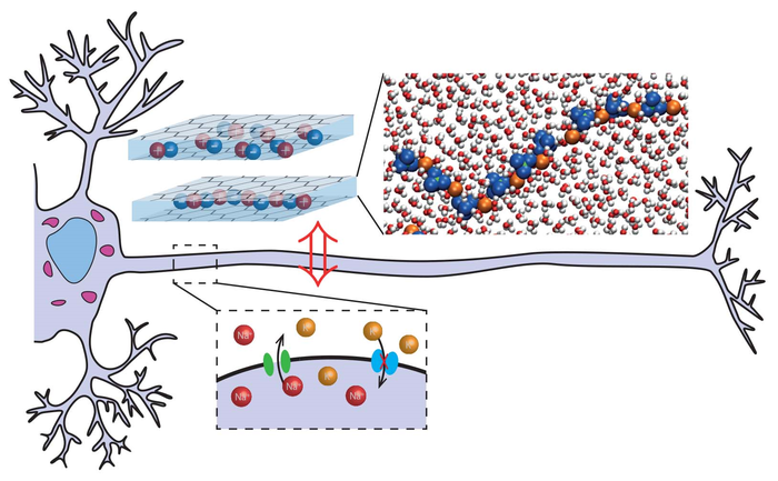
The platform the researchers developed consists of a graphene-based tunable THz resonator, with a gold-foil gate electrode forming a bottom reflective mirror. Above it, a graphene layer is book-ended with electrodes, forming a tunable top mirror. A non-volatile ionic liquid electrolyte layer sits between the mirrors, enabling control of the top mirror’s reflectivity by changing the applied voltage. In the middle of the device, between the mirrors, are molecules of alpha lactose, a sugar commonly found in milk.  

The system is controlled by two adjusters. One raises the lower mirror to change the length of the cavity — tuning the frequency of resonation to couple the light with the collective vibrational modes of the organic sugar molecules, which serve as a fixed number of oscillators for the system. The other adjuster changes the voltage applied to the top graphene mirror — altering the graphene’s reflective properties to transition the energy loss imbalances to adjust coupling strength. The delicate, fine tuning shifts weakly coupled terahertz light and organic molecules to become strongly coupled and vice versa.

“Exceptional points coincide with the crossover point between the weak and strong coupling regimes of terahertz light with collective molecular vibrations,” Özdemir said.

He noted that these singularity points are typically studied and observed in the coupling of analogous modes or systems, such as two optical modes, electronic modes or acoustic modes.

“This work is one of rare cases where exceptional points are demonstrated to emerge in the coupling of two modes with different physical origins,” Kocabas said. “Due to the topology of the exceptional points, we observed a significant modulation in the magnitude and phase of the terahertz light, which could find applications in next-generation THz communications.”

Unprecedented phase modulation in the THz spectrum

As the researchers apply voltage and adjust the resonance, they drive the system to an exceptional point and beyond. Before, at and beyond the exceptional point, the geometric properties — the topology — of the system change.

One such change is the phase modulation, which describes how a wave changes as it propagates and interacts in the THz field. Controlling the phase and amplitude of THz waves is a technological challenge, the researchers said, but their platform demonstrates unprecedented levels of phase modulation. The researchers moved the system through exceptional points, as well as along loops around exceptional points in different directions, and measured how it responded through the changes. Depending on the system’s topology at the point of measurement, phase modulation could range from zero to four magnitudes larger.

“We can electrically steer the device through an exceptional point, which enables electrical control on reflection topology,” said first author M. Said Ergoktas. “Only by controlling the topology of the system electronically could we achieve these huge modulations.” 

According to the researchers, the topological control of light-matter interactions around an exceptional point enabled by the graphene-based platform has potential applications ranging from topological optoelectronic and quantum devices to topological control of physical and chemical processes.

Contributors include Kaiyuan Wang, Gokhan Bakan, Thomas B. Smith, Alessandro Principi and Kostya S. Novoselov, University of Manchester; Sina Soleymani, graduate student in the Penn State Department of Engineering Science and Mechanics; Sinan Balci, Izmir Institute of Technology, Turkey; Nurbek Kakenov, who conducted work for this paper while at Bilkent University, Turkey.

I love the language in this press release, especially, ‘spectral singularities’. The explanations are more appreciated and help to make this image more than a pretty picture,

Caption: An international team, co-led by researchers at The University of Manchester’s National Graphene Institute (NGI) in the UK and the Penn State College of Engineering in the US, has developed a tunable graphene-based platform that allows for fine control over the interaction between light and matter in the terahertz (THz) spectrum to reveal rare phenomena known as exceptional points. The feat could contribute to the development of beyond-5G wireless technology for high-speed communication networks. Credit: Image Design, Pietro Steiner, The University of Manchester

Here’s a link to and a citation for the paper,

Topological engineering of terahertz light using electrically tunable exceptional point singularities by M. Said Ergoktas, Sina Soleymani, Nurbek Kakenov, Kaiyuan Wang, Thomas B. Smith, Gokhan Bakan, Sinan Balci, Alessandro Principi, Kostya S. Novoselov, Sahin K. Ozdemir, and Coskun Kocabas. Science • 7 Apr 2022 • Vol 376, Issue 6589 • pp. 184-188 • DOI: 10.1126/science.abn6528

This paper is behind a paywall.

Oddly, there is an identical press release dated April 8, 2022 on the Pennsylvania State University website with a byline for By Ashley J. WennersHerron and Alan Beck. Interestingly the first author is from Penn State and the second author is from the University of Manchester.

Graphene Week (September 5 – 9, 2022) is a celebration of 10 years of the Graphene Flagship

Back in 2013 the European Union announced two huge targeted research investments €1B each for the Graphene Flagship and the Human Brain Project to be distributed over 10 years. (I have an overview of the Graphene Flagship’s high points from 2013-15 in my April 22, 2016 posting.)

Now at the ten year mark and its final days, the Graphene Flagship is celebrating 10 years with a Graphene Week (from an August 30, 2022 Graphene Flagship press release on EurekAlert),

Graphene Week is a celebration of 10 years of the Graphene Flagship, a European Commission funded research project worth over €1 billion in funding. Held at BMW Welt — the exhibition space of one of the Graphene Flagship’s industrial partners based in Germany — the conference includes a comprehensive program of speakers, exhibitions, posters and a free pavilion.

The program includes a session on the European Chip Act, a notable point of debate for the continent. The act promises to mobilise more than €43 billion of both public and private investments to alleviate the global chip shortage. Graphene Week will demonstrate the potential of graphene-enabled alternatives to traditional semiconductors with the findings of the 2D-Experimental Pilot Line (2D-EPL).

The 2D-EPL is a €20 million project to integrate 2D materials into silicon wafers. The project has recently completed its first multi-project wafer (MPW) run, producing graphene integrated silicon wafers to academic and industrial customers.

During the conference Max Lemme of AMO GmbH in Germany and Sanna Arpiainen, of VTT Finland will discuss this subject along with the European Commission’s Thomas Skordas, Deputy Director General of DG CNECT and Bert De Colvenaer, Executive Director, KDT Joint Undertaking. Attendees can find the full program here.

The conference covers a large range of topics: from composites and medicine, to electronics and sensors. Beyond fundamental research, the talks by industry experts and European scientists will explore how graphene and related materials are disrupting critical European industries.

Graphene Week is co-chaired by Georg Duesberg from Bundeswehr University Munich and Elmar Bonaccurso, from Airbus Germany. In addition to Airbus, representatives from Lufthansa and other partners from the AEROGrAFT project will be in attendance, showcasing their graphene air filtration application for aircraft.   aircraft. 

Graphene Week will also host its Graphene Innovation Forum, a dedicated space for scientists to meet those in industry. Interactive panel discussions with industrial representatives will dive into future trends of graphene applications. The Innovation forum will feature speakers from both the Graphene Flagship’s large industrial partners including Medica, Lufthansa, Nokia and Airbus and smaller companies including Graphene Flagship spin-offs Emberion, BeDimensional and Qurv.

The Open Forum will collate some of the leading experts of the Graphene Flagship for a panel discussion on the success of graphene research and innovation where the audience is encouraged to ask questions. And the Diversity in Graphene initiative will offer a panel discussion focused on career development and professional use of social media.

The Graphene Flagship welcomes the public to explore the Graphene Pavilion in BMW Welt. The exhibition will showcase applications for graphene for cars, planes, phones and cities, together with product demos and videos. This pavilion will be free and open to the public from 9am on Friday 9 September to 6pm on Sunday 11 September.

“The Graphene Flagship is one of the largest ever EU projects, forming a network of 171 academic and industrial partners from 22 countries,” explained Jari Kinaret, Director of the Graphene Flagship. “In the 17th  edition, Graphene Week provides an opportunity to demonstrate the successes of the project and the ongoing legacy it will have on Europe’s industry. We look forward to welcoming our academic and industrial partners to join us in Munich for this celebration.”

More information on Graphene Week, access to the speaker line up and full scientific program can be found on the Graphene Flagship website. Registration provides access to all scientific sessions, sponsored sessions, access to the exhibition, conference material and more. To register click here.

This is the BMW Welt,

Looks like something out of a science fiction movie, eh?

You can find (Graphene Flagship spinoff companies), Emberion website here, BeDimensional website here, and Qurv Technologies website here.

A graphene-inorganic-hybrid micro-supercapacitor made of fallen leaves

I wonder if this means the end to leaf blowers. That is almost certainly wishful thinking as the researchers don’t seem to be concerned with how the leaves are gathered.

The schematic illustration of the production of femtosecond laser-induced graphene. Courtesy of KAIST

A January 27, 2022 news item on Nanowerk announces the work (Note: A link has been removed),

A KAIST [Korea Advanced Institute of Science and Technology] research team has developed graphene-inorganic-hybrid micro-supercapacitors made of fallen leaves using femtosecond laser direct laser writing (Advanced Functional Materials, “Green Flexible Graphene-Inorganic-Hybrid Micro-Supercapacitors Made of Fallen Leaves Enabled by Ultrafast Laser Pulses”).

A January 27, 2022 KAIST press release (also on EurekAlert but published January 26, 2022), which originated the news item, delves further into the research,

The rapid development of wearable electronics requires breakthrough innovations in flexible energy storage devices in which micro-supercapacitors have drawn a great deal of interest due to their high power density, long lifetimes, and short charging times. Recently, there has been an enormous increase in waste batteries owing to the growing demand and the shortened replacement cycle in consumer electronics. The safety and environmental issues involved in the collection, recycling, and processing of such waste batteries are creating a number of challenges.

Forests cover about 30 percent of the Earth’s surface and produce a huge amount of fallen leaves. This naturally occurring biomass comes in large quantities and is completely biodegradable, which makes it an attractive sustainable resource. Nevertheless, if the fallen leaves are left neglected instead of being used efficiently, they can contribute to fire hazards, air pollution, and global warming.

To solve both problems at once, a research team led by Professor Young-Jin Kim from the Department of Mechanical Engineering and Dr. Hana Yoon from the Korea Institute of Energy Research developed a novel technology that can create 3D porous graphene microelectrodes with high electrical conductivity by irradiating femtosecond laser pulses on the leaves in ambient air. This one-step fabrication does not require any additional materials or pre-treatment. 

They showed that this technique could quickly and easily produce porous graphene electrodes at a low price, and demonstrated potential applications by fabricating graphene micro-supercapacitors to power an LED and an electronic watch. These results open up a new possibility for the mass production of flexible and green graphene-based electronic devices.

Professor Young-Jin Kim said, “Leaves create forest biomass that comes in unmanageable quantities, so using them for next-generation energy storage devices makes it possible for us to reuse waste resources, thereby establishing a virtuous cycle.” 

This research was published in Advanced Functional Materials last month and was sponsored by the Ministry of Agriculture Food and Rural Affairs, the Korea Forest Service, and the Korea Institute of Energy Research.

Here’s a link to and a citation for the paper,

Green Flexible Graphene–Inorganic-Hybrid Micro-Supercapacitors Made of Fallen Leaves Enabled by Ultrafast Laser Pulses by Truong-Son Dinh Le, Yeong A. Lee, Han Ku Nam, Kyu Yeon Jang, Dongwook Yang, Byunggi Kim, Kanghoon Yim, Seung-Woo Kim, Hana Yoon, Young-Jin Kim. Advanced Functional Materials DOI: https://doi.org/10.1002/adfm.202107768 First published: 05 December 2021

This paper is behind a paywall.

Graphene: a long story

For a change this October 19, 2021 item on phys.org isn’t highlighting a single research paper so much as it provides a history of graphene and context for research being done at the Joint Quantum Institute (JQI) at the University of Maryland (US),

Carbon is not the shiniest element, nor the most reactive, nor the rarest. But it is one of the most versatile.

Carbon is the backbone of life on earth and the fossil fuels that have resulted from the demise of ancient life. Carbon is the essential ingredient for turning iron into steel, which underlies technologies from medieval swords to skyscrapers and submarines. And strong, lightweight carbon fibers are used in cars, planes and windmills. Even just carbon on its own is extraordinarily adaptable: It is the only ingredient in (among other things) diamonds, buckyballs and graphite (the stuff used to make pencil lead).

This last form, graphite, is at first glance the most mundane, but thin sheets of it host a wealth of uncommon physics. Research into individual atom-thick sheets of graphite—called graphene—took off after 2004 when scientists developed a reliable way to produce it (using everyday adhesive tape to repeatedly peel layers apart). In 2010 early experiments demonstrating the quantum richness of graphene earned two researchers the Nobel Prize in physics.

In recent years, graphene has kept on giving. Researchers have discovered that stacking layers of graphene two or three at a time (called, respectively, bilayer graphene or trilayer graphene) and twisting the layers relative to each other opens fertile new territory for scientists to explore. Research into these stacked sheets of graphene is like the Wild West, complete with the lure of striking gold and the uncertainty of uncharted territory.

Researchers at JQI and the Condensed Matter Theory Center (CMTC) at the University of Maryland, including JQI Fellows Sankar Das Sarma and Jay Sau and others, are busy creating the theoretical physics foundation that will be a map of this new landscape. And there is a lot to map; the phenomena in graphene range from the familiar like magnetism to more exotic things like strange metallicity, different versions of the quantum Hall effect, and the Pomeranchuk effect—each of which involve electrons coordinating to produce unique behaviors. One of the most promising veins for scientific treasure is the appearance of superconductivity (lossless electrical flow) in stacked graphene.

“Here is a system where almost every interesting quantum phase of matter that theorists ever could imagine shows up in a single system as the twist angle, carrier density, and temperature are tuned in a single sample in a single experiment,” says Das Sarma, who is also the Director of the CMTC. “Sounds like magic or science fantasy, except it is happening every day in at least ten laboratories in the world.”

The richness and diversity of the electrical behaviors in graphene stacks has inspired a stampede of research. The 2021 American Physical Society March Meeting included 13 sessions addressing the topics of graphene or twisted bilayers, and Das Sarma hosted a day long virtual conference in June for researchers to discuss twisted graphene and the related research inspired by the topic. The topic of stacked graphene is extensively represented in scientific journals, and the online arXiv preprint server has over 2,000 articles posted about “bilayer graphene”—nearly 1,000 since 2018.

Perhaps surprisingly, graphene’s wealth of quantum research opportunities is tied to its physical simplicity.

An October 18, 2021 JQI news release by Bailey Bedford, which originated the news item, explains why researchers have described a twist found in graphene as ‘magic’,

Researchers have discovered that at a special, small twist angle (about 1.1 degrees)—whimsically named the “magic angle”—the environment is just right to create strong interactions that radically change its properties. When that precise angle is reached, the electrons tend to cluster around certain areas of the graphene, and new electrical behaviors suddenly appear as if summoned with a dramatic magician’s flourish. Magic angle graphene behaves as a poorly-conducting insulator in some circumstances and in other cases goes to the opposite extreme of being a superconductor—a material that transports electricity without any loss of energy.

The discovery of magic-angle graphene and that it has certain quantum behaviors similar to a high-temperature superconductor was the Physics World 2018 Breakthrough of the Year. Superconductors have many valuable potential uses, like revolutionizing energy infrastructure and making efficient maglev trains. Finding a convenient, room-temperature superconductor has been a holy grail for scientists.

I haven’t done to justice to this piece and, so, for anyone interested in graphene, superconductors, and electronics I recommend reading the piece (October 18, 2021 JQI news release by Bailey Bedford) in its entirety where you’ll also find references to these articles and more,

Reference Publication

Related JQI Articles

Sticky tape, hackers, and quantum communications

I always appreciate a low technology solution to a problem. In this case, it’s a piece of sticky tape which halts compute hackers in their tracks. Here’s more from an August 30, 2021 University of Technology Sydney press release (also on EurekAlert but published August 26, 2021), Note: Links have been removed,

Researchers from the University of Technology Sydney (UTS) and TMOS, an Australian Research Council Centre of Excellence [specifically, the Australian Research Council Centre of Excellence for Transformative Meta-Optical Systems (TMOS)], have taken the fight to online hackers with a giant leap towards realizing affordable, accessible quantum communications, a technology that would effectively prevent the decryption of online activity. Everything from private social media messaging to banking could become more secure due to new technology created with a humble piece of adhesive tape.

Quantum communication is still in its early development and is currently feasible only in very limited fields due to the costs associated with fabricating the required devices. The TMOS researches have developed new technology that integrates quantum sources and waveguides on chip in a manner that is both affordable and scalable, paving the way for future everyday use.

The development of fully functional quantum communication technologies has previously been hampered by the lack of reliable quantum light sources that can encode and transmit the information.

In a paper published today in ACS Photonics, the team describes a new platform to generate these quantum emitters based on hexagonal boron nitride, also known as white graphene. Where current quantum emitters are created using complex methods in expensive clean rooms, these new quantum emitters can be created using $20 worth of white graphene pressed on to a piece of adhesive tape.

These 2D materials can be pressed onto a sticky surface such as the [sic] adhesive tape [emphasis mine] and exfoliated, which is essentially peeling off the top layer to create a flex. Multiple layers of this flex can then be assembled in a Lego-like style, offering a new bottom up approach as a substitute for 3D systems.

TMOS Chief Investigator Igor Aharonovich said: “2D materials, like hexagonal boron nitride, are emerging materials for integrated quantum photonics, and are poised to impact the way we design and engineer future optical components for secured communication.”

In addition to this evolution in photon sources, the team has developed a high efficiency on-chip waveguide, a vital component for on-chip optical processing.

Lead author Chi Li said: “Low signal levels have been a significant barrier preventing quantum communications from evolving into practical, workable models. We hope that with this new development, quantum comms will become an everyday technology that improves people’s lives in new and exciting ways.”

Here’s a link to and a citation for the paper,

Integration of hBN Quantum Emitters in Monolithically Fabricated Waveguides by Chi Li, Johannes E. Fröch, Milad Nonahal, Thinh N. Tran, Milos Toth, Sejeong Kim, and Igor Aharonovich. ACS Photonics 2021, XXXX, XXX, XXX-XXX DOI: https://doi.org/10.1021/acsphotonics.1c00890 Publication Date:August 20, 2021 © 2021 American Chemical Society

This paper is behind a paywall.

Sticky or adhesive tape is part of graphene lore and seems to exert a great fascination for scientists as I note in my June 12, 2018 posting.

Artificial ionic neuron for electronic memories

This venture into brain-like (neuromorphic) computing comes from France according to an August 17, 2021 news item on Nanowerk (Note: A link has been removed),

Brain-inspired electronics are the subject of intense research. Scientists from CNRS (Centre national de la recherche scientifique; French National Centre for Scientific Research) and the Ecole Normale Supérieure – PSL have theorized how to develop artificial neurons using, as nerve cells, ions to carry the information.

Their work, published in Science (“Modeling of emergent memory and voltage spiking in ionic transport through angstrom-scale slits”), reports that devices made of a single layer of water transporting ions within graphene nanoslits have the same transmission capacity as a neuron.

Caption Artificial neuron prototype: nanofluidic slits can play the role of ion channels and allow neurons to communicate. Ion clusters achieve the ion transport that causes this communication. Credit © Paul Robin, ENS Laboratoire de Physique (CNRS/ENS-PSL/Sorbonne Université/Université de Paris).

Au August 16, 2021 CNRS press release (also on EurekAlert but published August 6, 2021), which originated the news item, provides insight into the international interest in neuromorphic computing along with a few technical details about this latest research,

With an energy consumption equivalent to two bananas per day, the human brain can perform many complex tasks. Its high energy efficiency depends in particular on its base unit, the neuron, which has a membrane with nanometric pores called ion channels, which open and close according to the stimuli received. The resulting ion flows create an electric current responsible for the emission of action potentials, signals that allow neurons to communicate with each other.

Artificial intelligence can do all of these tasks but only at the cost of energy consumption tens of thousands of times that of the human brain. So the entire research challenge today is to design electronic systems that are as energy efficient as the human brain, for example, by using ions, not electrons, to carry the information. For this, nanofluidics, the study of how fluids behave in channels less than 100 nanometers wide, offer many perspectives. In a new study, a team from the ENS Laboratoire de Physique (CNRS/ENS-PSL/Sorbonne Université/Université de Paris) shows how to construct a prototype of an artificial neuron formed of extremely thin graphene slits containing a single layer of water molecules1. The scientists have shown that, under the effect of an electric field, the ions from this layer of water assemble into elongated clusters and develop a property known as the memristor effect: these clusters retain some of the stimuli that have been received in the past. To repeat the comparison with the brain, the graphene slits reproduce the ion channels, clusters and ion flows. And, using theoretical and digital tools, scientists have shown how to assemble these clusters to reproduce the physical mechanism of emission of action potentials, and thus the transmission of information.

This theoretical work continues experimentally within the French team, in collaboration with scientists from the University of Manchester (UK). The goal now is to prove experimentally that such systems can implement simple learning algorithms that can serve as the basis for tomorrow’s electronic memories.

1 Recently invented in Manchester by the group of André Geim (Nobel Prize in Physics 2010)

Here’s a link to and a citation for the paper,

Modeling of emergent memory and voltage spiking in ionic transport through angstrom-scale slits by Paul Robin, Nikita Kavokine, Lydéric Bocquet. Science 06 Aug 2021: Vol. 373, Issue 6555, pp. 687-691 DOI: 10.1126/science.abf7923

This paper is behind a paywall.

Season’s Greetings with the world’s thinnest Christmas tree

Courtesy: Technical University of Denmark

I haven’t seen one of these in a while. It used to be a relatively common occurrence (especially during a holiday) that scientists would create the world’s smallest XXX and send a press release. I’ve missed them so I’m glad to see this one pop up.

A December 23, 2021 news item on phys.org announces the world’s thinnest Christmas tree,

A Christmas tree with a thickness of one atom has been made at DTU [Technical University of Denmark]. It shows how terahertz measurements can be used to ensure the quality of graphene.

A December 22, 2021 DTU press release by by Tore Vind Jensen, which originated the news item, provides more technical detail,

The Christmas tree in the pictures above is 14 centimeters long. Since it is made of graphene, it consists of carbon atoms in only one layer and is only a third of a nanometer thick. It is cut out of a 10-meter long roll of graphene, transferred in one piece using a rebuilt laminating machine and then scanned with terahertz radiation.

The experiment shows that continuous quality control can be done during the production of graphene, which is expected to play a significant role in future high-speed electronics, i.e. medical instruments and sensors.

Graphene is a so-called two-dimensional material, i.e. it consists of atoms in one cohesive layer that is only one atom thin. It is more robust, stiffer and better at conducting electricity and heat than any other material we know of. Therefore, graphene is an obvious candidate for electronic circuits that take up less space, weigh less, are bendable and are more efficient than the electronics we know today.

“Even if you could make a pencil drawing of a Christmas tree and lift it off the paper—which, figuratively, is what we have done—it would be much thicker than one atom. A bacterium is, e.g. 3000 times thicker than the graphene layer we used. That’s why I dare call this the world’s thinnest Christmas tree. And although the starting point is carbon, just like the graphite in a pencil, graphene is at the same time even more conductive than copper. The “drawing” is made in one perfect layer in one piece, ” says Professor Peter Bøggild who lead the team behind the Christmas tree experiment.

“But behind the Christmas joke hides an important breakthrough. For the first time, we managed to make an in-line quality control of the graphene layer while we transferred it. Doing this is the key to gaining stable, reproducible and usable material properties, which is the prerequisite for utilizing graphene in, e.g. electronic circuits.”

30,000 times thinner than kitchen film

As the researchers have done in this case, the graphene can be “grown” on copper film. The graphene is deposited on a roll of copper foil at around 1000 ° C. That process is well known and well-functioning. But a lot can go wrong when the ultra-thin graphene film is moved from the copper roller to where it is used. Since graphene is 30,000 times thinner than kitchen film, it is a demanding process. Researcher Abhay Shivayogimath has been behind several new inventions in DTU’s transfer process, ensuring a stable transfer of the graphene layers from the copper roll.

Moreover, there has been no technology that could control the electrical quality of graphene on the go—while transferring it. This year Peter Bøggild and his colleague Professor Peter Uhd Jepsen from DTU Fotonik, one of the world’s leading terahertz researchers, established a way to do it.

The colored images are measurements of how the graphene layer absorbs terahertz radiation. The absorption is directly related to the electric conductivity: the better the conductive graphene, the better it absorbs.

Terahertz rays are high-frequency radio waves that lie between infrared radiation and microwaves. Like X-rays, they can be used to scan human bodies, as we know it from airport security. Terahertz rays can also take pictures of the electrical resistance of the graphene layer. By connecting the terahertz scanner to the machine that transfers the graphene film, it is possible to image the electrical properties of the film during the transfer process.

Official international measurement standard

Suppose the implementation of graphene and other 2D materials is to be accelerated. In that case, ongoing quality assurance is a prerequisite, says Peter Bøggild. Quality control precedes trust, he says. The technology can guarantee that graphene-based technologies are manufactured more uniformly and predictably with fewer errors. This year, the DTU researchers’ method was approved as the first official international measurement standard for graphene. Their method was described earlier this year in the article ‘Terahertz imaging of graphene paves the way to industrialisation.’

The potential is excellent. Graphene and other two-dimensional materials can e.g. enable the manufacturing of high-speed electronics performing lightning-fast calculations with far less power consumption than the technologies we use today. But before graphene can become more widespread on an industrial scale and be used in electronics, we encounter in everyday life three main problems must be solved.

First, the price is too high. More and faster production is needed to bring the price down. But with that, you face the second problem: When you increase the speed and can not at the same time check the quality, the risk of error also increases dramatically. At high high-speed transfer, everything must be set precisely.This brings us to the third problem: How do you know what is precise?

It requires measurements. And preferably measurements during the actual transfer process. The DTU team is convinced that the best bet on that method is quality control using terahertz radiation.

Peter Bøggild emphasizes that these three problems have not been solved with the new method alone: “We have taken a very significant step. We have converted a laminating machine into a so-called roll-2-roll transfer system. It gently lifts the graphene layer from the copper roll on which the graphene layer is grown and moves it onto plastic foil without it breaking, becoming wrinkled or dirty. When we combine this with the terahertz system, we can immediately see if the process has gone well. That is, whether we have unbroken graphene with low electrical resistance,” says Peter Bøggild.

Joyeux Noël et une bonne année 2022!

Radiation-free quantum technology with graphene

A July 8, 2021 news item on Nanowerk announces research from Finland and Switzerland that could have an impact on real world quantum technologies (Note: A link has been removed),

Rare-earth compounds have fascinated researchers for decades due to the unique quantum properties they display, which have so far remained totally out of reach of everyday compounds. One of the most remarkable and exotic properties of those materials is the emergence of exotic superconducting states, and particularly the superconducting states required to build future topological quantum computers.

While these specific rare-earth compounds, known as heavy fermion superconductors, have been known for decades, making usable quantum technologies out of them has remained a critically open challenge. This is because these materials contain critically radioactive compounds, such as uranium and plutonium, rendering them of limited use in real-world quantum technologies.

New research has now revealed an alternative pathway to engineer the fundamental phenomena of these rare-earth compounds solely with graphene, which has none of the safety problems of traditional rare-earth compounds.

The exciting result in the new paper shows how a quantum state known as a “heavy fermion” can be produced by combining three twisted graphene layers. A heavy fermion is a particle – in this case an electron – that behaves like it has a lot more mass than it actually does. The reason it behaves this way stems from unique quantum many-body effects that were mostly only observed in rare-earth compounds until now.

This heavy fermion behavior is known to be the driving force of the phenomena required to use these materials for topological quantum computing. This new result demonstrates a new, non-radioactive way of achieving this effect using only carbon, opening up a pathway for sustainably exploiting heavy fermion physics in quantum technologies.

A July 8, 2021 Aalto University press release (also on EurekAlert), which originated the news item, provides more details,

In the paper authored by Aline Ramires, (Paul Scherrer Institute, Switzerland) and Jose Lado (Aalto University), the researchers show how it is possible to create heavy fermions with cheap, non-radioactive materials. To do this, they used graphene, which is a one-atom thick layer of carbon. Despite being chemically identical to the material that is used in regular pencils, the sub-nanometre thickness of graphene means that it has unexpectedly unique electrical properties. By layering the thin sheets of carbon on top of one another in a specific pattern, where each sheet is rotated in relation to the other, the researchers can create the quantum properties effect that results in the electrons in the graphene behaving like heavy fermions.

“Until now, practical applications of heavy fermion superconductors for topological quantum computing has not been pursued much, partially because it required compounds containing uranium and plutonium, far from ideal for applications due to their radioactive nature”, says Professor Lado, “In this work we show that one can aim to realize the exactly very same physics just with graphene. While in this work we only show the emergence of heavy fermion behavior, addressing the emergence of topological superconductivity is a natural next step, which could potentially have a groundbreaking impact for topological quantum computing.”

Topological superconductivity is a topic of critical interest for quantum technologies, also tackled by alternative strategies in other papers from Aalto University Department of Applied Physics, including a previous paper by Professor Lado. “These results potentially provide a carbon-based platform for exploitation of heavy fermion phenomena in quantum technologies, without requiring rare-earth elements”, concludes Professor Lado.

Here’s a link to and a citation for the paper,

Emulating Heavy Fermions in Twisted Trilayer Graphene by Aline Ramires and Jose L. Lado. Phys. Rev. Lett. 127, 026401 DOI: https://doi.org/10.1103/PhysRevLett.127.026401 Published 7 July 2021 © 2021 American Physical Society

This paper is behind a paywall.

Quick and efficient nanographene synthesis

Thank you to Nagoya University (Japan) for making this image available.

Caption: APEX reactions are carried out on the K, M and bay regions of the polycyclic aromatic hydrocarbon, synthesizing multiple nanographenes. These reactions can then be repeated, further increasing the number of potential nanographene structures that can be synthesized. Credit: Issey Takahashi

From a June 28, 2021 Nagoya University press release (also on EurekAlert),

A group of researchers at Nagoya University, Japan, have developed a new method for quickly and efficiently synthesizing nanographenes, a type of nanocarbon with great potential as a next generation material.

Nanographenes are the part structures of graphene, which is a sheet of carbon atoms around 3 nanometers thick with particular potential for use in semiconductor development, having electron mobility several hundred times better than current generation materials. Graphene was first isolated in 2004, a discovery which received the 2010 Nobel Prize in physics, making it a very new material which is currently the subject of a great deal of research.

With magnetic and electric characteristics beyond those of graphene, nanographenes are equally of interest to scientists in the nanocarbon research field. The biggest obstacle, albeit an exciting one, faced by researchers is the sheer number of potential nanographenes. The number of potentially possible nanographene structures increases with the number of benzene rings (6 atoms of carbon in a hexagonal formation) to make them. For example, even a relatively small 10 benzene ring nanographene may have up to 16,000 variants. As each nanographene has different physical characteristics, the key to applied nanographene research is to identify the relationship between the structure and characteristics of as many nanographenes as possible.

Thus, scientists’ task is to create a nanographene library, containing data on the properties of as many nanographenes as possible. However, the current method of nanographene synthesis, known as a coupling reaction, is a multi-step process which produces one single nanographene. Thus, to create a 100-nanographene library, 100 separate coupling reactions would have to be carried out. Even this would be a significant undertaking, rendering the construction of a truly comprehensive nanographene library practically impossible.

To solve this problem, the Nagoya University research group, led by Professor Kenichiro Itami, have been working on the APEX reaction, a reaction which uses polycyclic aromatic hydrocarbons as templates to synthesize nanographenes. Polycyclic aromatic hydrocarbons have three areas of their structure – known as the K region, M region and bay region – which can be elongated in an APEX reaction, producing three nanographenes. These nanographenes can then be further elongated in a second reaction, meaning that a large number of nanographenes can be synthesized from a single polycyclic aromatic hydrocarbon template molecule.

With Professor Itami’s group having already developed the K region APEX reaction, and another group of scientists having done so for the bay region, they turned their attention to the M region. They activated the M region using the 1950 Nobel Prize winning Diels-Alder reaction, and succeeded in carrying out an elongation reaction on the activated M region, thus rendering all three possible sites on the polycyclic aromatic hydrocarbons capable of synthesizing nanographenes.

The researchers were able to produce 13 nanographenes with three APEX reactions, with most of these being previously unseen structures, thus proving both the efficiency and usefulness of this new method.

This exciting new piece of research and its potential to accelerate the creation of nanographene libraries is a step towards the development of the next generation of materials, which have the potential to revolutionize semiconductors and solar energy and improve lives all around the world.

Here’s a link to and a citation for the paper,

Diversity-oriented synthesis of nanographenes enabled by dearomative annulative π-extension by Wataru Matsuoka, Hideto Ito, David Sarlah & Kenichiro Itami. Nature Communications volume 12, Article number: 3940 (2021) DOI: https://doi.org/10.1038/s41467-021-24261-y Published 24 June 2021

This paper is open access.

Graphene in art preservation and restoration

A July 5, 2021 news item on phys.org announces a new technology for preserving and restoring your paintings,

The exposure of colors used in artworks to ultraviolet (UV) and visible light in the presence of oxidizing agents triggers color degradation, fading and yellowing. These degradation mechanisms can lead to irreversible alteration of artworks. Protective varnishes and coatings currently used to protect art paintings are not acceptable solutions, since their removal requires the use of solvents, which can affect adversely the underlying work surface.

A team of researchers from the Institute of Chemical Engineering Sciences of Foundation for Research and Technology-Hellas (FORTH/ ICE-HT), the Department of Chemical Engineering of the University of Patras, and the Center for Colloid and Surface Science (CSGI) of the University of Florence, led by Professor Costas Galiotis, had the innovative ideato use graphene veils for the protection of paintings against environmental degradation.

A July 2, 2021 Foundation for Research and Technology – Hellas (FORTH) press release, which originated the news item, provides more details,

Since its isolation in 2004 by Geim [Andre Geim] and Novoselov [Konstantin Novoselov] from the University of Manchester (Nobel Prize in Physics in 2010), graphene has been termed as a ‘wonder material’ due to its exceptional properties that have already been used in many applications and products. The graphene veil used in this work is a flexible, transparent film, produced by the technique of chemical vapor deposition. It has a monoatomic thickness and, since there are no size limitations in the other dimensions (length and width), it can cover any required large surface areas.

The results from measurements performed in the above mentioned laboratories, showed that this membrane is impermeable to moisture, the oxidizing agents and other harmful pollutants and also can absorb a large amount of harmful ultraviolet radiation. Finally, in contrast to other protective means, it is demonstrated that these graphene coatings are relatively easy to remove without damaging the surface of the artworks.

[downloaded from https://phys.org/news/2021-07-graphene-paving-methods-art.html]

Before getting to the link and citation for the paper, here’s the abstract, which helps fill n a few more details,

Modern and contemporary art materials are generally prone to irreversible colour changes upon exposure to light and oxidizing agents. Graphene can be produced in thin large sheets, blocks ultraviolet light, and is impermeable to oxygen, moisture and corrosive agents; therefore, it has the potential to be used as a transparent layer for the protection of art objects in museums, during storage and transportation. Here we show that a single-layer or multilayer graphene veil, produced by chemical vapour deposition, can be deposited over artworks to protect them efficiently against colour fading, with a protection factor of up to 70%. We also show that this process is reversible since the graphene protective layer can be removed using a soft rubber eraser without causing any damage to the artwork. We have also explored a complementary contactless graphene-based route for colour protection that is based on the deposition of graphene on picture framing glass for use when the directapplication of graphene is not feasible due to surface roughness or artwork fragility. Overall, the present results are a proof of concept of the potential use of graphene as an effective and removable protective advanced material to prevent colour fading in artworks.

And now, a link to and a citation for the paper,

Preventing colour fading in artworks with graphene veils by M. Kotsidi, G. Gorgolis, M. G. Pastore Carbone, G. Anagnostopoulos, G. Paterakis, G. Poggi, A. Manikas, G. Trakakis, P. Baglioni & C. Galiotis. Nature Nanotechnology (2021) DOI: https://doi.org/10.1038/s41565-021-00934-z Published 01 July 2021

This paper is behind a paywall.