First the fun (*ETA: June 17, 2016: Sadly, this video no longer seems to be freely available but there is an updated version in my June 17, 2016 posting about the provisional names for four new elements.),
You may to want to check out Jennifer Miller’s May 20, 2013 Fast Company article about this effort where she highlights one of the cheekier illustrations in this periodic table of elements song from AsapSCIENCE (Mitchell Moffit and Gregory Brown).
I found out more about AsapSCIENCE and the duo (former classmates at the University of Guelph in Ontario, Canada) in a Sept. 18, 2012 article by Chase Hoffberger for the Daily Dot,
Mitchell Moffit and Gregory Brown are the two former University of Guelph classmates behind asapSCIENCE, a young but massively informative and entertaining YouTube channel that produces three-minute lessons on all the scientific questions that you actually want answered: “The Scientific Power of Naps.” …
“We’re trying to keep a balance of the things that people want to know as well as cool tidbits that people would never have any idea about,” Moffit, 23, told the Daily Dot from his home in Ontario, where he holds down production and most video voiceovers while Brown spends the year teaching science in England.
…
“We’re interested in inspiring people who maybe don’t know a lot about science and think of it as this hard subject in school,” Moffit said.
The perfect example’s “The Science of Orgasms,” which more than 380,000 people have viewed in the past week and comes packed with far more knowledge and insight than the time your dad tried to put a condom on a cucumber.
At the time of the Daily Dot article (Sept. 2012), AsapSCIENCE had been making videos for three months and already had more than 40,000 subscribers on their YouTube channel. After checking this morning (May 21, 2013), I see the channel has over 784,000 subscribers. Bravo!
I have written about the periodic table of elements before. This Feb. 8, 2012 posting features Daniel Radcliffe (Harry Potter) singing Tom Lehrer’s classic Periodic Table of Elements song.
Cornell researchers Jenny Sabin, assistant professor of architecture, and Dan Luo, professor of biological and environmental engineering, are among the lead investigators on a new research project to produce “buildable, bendable and biological materials” for a wide range of applications.
…
The project is intended to bring new ideas, motifs, portability and design to the formation of intricate chemical, biological and architectural materials.
Based on Kirigami (from the Japanese word kiru, “to cut”), the project “offers a previously unattainable level of design, dynamics and deployability” to self-folding and unfolding materials from the molecular scale to the architectural level, according to the researchers.
The project is intended to illuminate new principles of architecture, materials synthesis and biological structures, and advance several technologies – including meta-materials, sensors, stealth aircraft and adaptive and sustainable buildings. A complementary goal is to generate public interest through an enhanced impact on science, art and engineering.
“Like the opening and closing of flowers, satellites and even greeting cards, our research will offer a rich and diverse set of intricate surprises, problems and challenges for students at all levels, and broaden their interest and awareness of emerging science and engineering,” according to the project proposal, “Cutting and Pasting: Kirigami in Architecture, Technology and Science” (KATS).
The Emerging Frontiers in Research Innovation grant from the NSF is in the research category of Origami Design for Integration of Self-assembling Systems for Engineering Innovation.
I wish they had a few sample illustrations of how this project might look as a macroscale architectural (or other type of) project even it is a complete fantasy.
As I recall it’s Robbie Burns who coined the phrase, ‘the gift to see ourselves as others see us’, and it’s the Globe and Mail newspaper in its May 17, 2013 article (Jason Kenney visits California to lure tech workers north) which provides that perspective in a quote about Minister of Immigration, Jason Kenney’s current tour promoting Canada’s special Startup Visa,
“The Canadian perspective is they would love to re-create Silicon Valley in Canada,” said Irene Bloemraad, a professor who chairs the Canadian studies program at UC Berkeley. “And they recognize that under the current immigration system in the United States … there are people who are having a hard time getting permanent legal status.”
Anirudh Bhattacharyya writing for the Hindustan Times about Kenney’s tour and this latest effort to attract entrepreneurs to Canada notes in a May 16, 2013 article,
As Canada’s minister for citizenship, immigration and multiculturalism Jason Kenney heads to California’s Silicon Valley for four days, pushing the country’s new Startup Visa programme, he will make an appearance at TiECon 2013, the annual conference of The Indus Entrepreneurs [TIE], dominated by tech pioneers of Indian origin.
Minister Kenney will arrive in Silicon Valley on Friday [May 17, 2013], and will even be present at a Canadian government booth at the Santa Clara convention venue for TiECon, as part of an attempt to poach entrepreneurial talent in the tech sector away from the United States.
In an interview with the Hindustan Times, the minister said, “I think it’s no secret that many of the bright young people (in America) on short term work permits, are of Asian origin and more specifically of Indian origin.”
Canada’s Startup Visa program is similar to other efforts in Australia and the UK and it traces its own origins to a US initiative, from the Bhattacharyya article,
Ironically, the idea for the visa originated with the Canadian venture capital industry observing movement in the US Congress in recent years to create an American startup visa. That effort has yet to succeed. The industry then promoted the concept in Canada.
It’s not all roses and sunshine for entrepreneurs who wish to come to Canada although there is one major upside unique to the Canadian effort according to CICS Immigration Consulting’s May 17, 2013 posting on their website,
Citizenship and Immigration Canada (CIC) hopes to capitalize on the frustration tech companies in the U.S. are feeling over immigration restrictions on foreign technology workers and encourage them to relocate to and invest in Canada.
The eventual goal is to help foster the development of a Canadian equivalent to Silicon Valley.
One challenge that CIC faces in this mission is the country’s top marginal income tax rate, which is significantly higher than that of the U.S. A Canadian entrepreneur can look forward to paying about 50 percent of their income to the government if they succeed in joining the top bracket of income earners. [emphasis mine]
Compensating for this disadvantage, the federal government is offering a perk that no other advanced economy offers foreign entrepreneurs: permanent residency status. [emphasis mine]
I suppose this is one way of developing an entrepreneurial and innovative culture in Canada but it seems to me that if other conditions (financing, willingness to take risks, appropriate governmental regulations, etc.) are not met, this may cause yet more problems.
As to whether or not creating a ‘Silicon Valley’ in Canada is possible or even desirable, I don’t know. There is only one Louvre, one Terra Cotta army, one Borobudur, one Stonehenge, one Mount Olympus, one Grand Canyon, one Guggenheim, etc. Of course, there are other art museums, other funerary displays, and other wonders but there is always the one which holds precedence and retains its grip on the imagination in a way the others do not. Canadians can try to copy the US’s Silicon Valley but if our effort is to be successful, we must find a way to put our own stamp on it and we need to recognize that it may always stand in the shadow of its parent.
There’s perfection and then there’s imperfection in this story about the nanoscale. From the May 19, 2013 news release on EurekAlert,
One of the basic principles of nanotechnology is that when you make things extremely small—one nanometer is about five atoms wide, 100,000 times smaller than the diameter of a human hair—they are going to become more perfect.
“Perfect in the sense that their arrangement of atoms in the real world will become more like an idealized model,” says University of Vermont engineer Frederic Sansoz, “with smaller crystals—in for example, gold or copper—it’s easier to have fewer defects in them.”
And eliminating the defects at the interface separating two crystals, or grains, has been shown by nanotechnology experts to be a powerful strategy for making materials stronger, more easily molded, and less electrically resistant—or a host of other qualities sought by designers and manufacturers.
Scientists thought they’d found perfection in 2004 (from the news release),
Since 2004, when a seminal paper came out in Science, materials scientists have been excited about one special of arrangement of atoms in metals and other materials called a “coherent twin boundary” or CTB.
Based on theory and experiment, these coherent twin boundaries are often described as “perfect,” appearing like a perfectly flat, one-atom-thick plane in computer models and electron microscope images.
Over the last decade, a body of literature has shown these coherent twin boundaries—found at the nanoscale within the crystalline structure of common metals like gold, silver and copper—are highly effective at making materials much stronger while maintaining their ability to undergo permanent change in shape without breaking and still allowing easy transmission of electrons—an important fact for computer manufacturing and other electronics applications.
It turns out that not all coherent twin boundaries are ‘perfect’ (from the news release),
A team of scientists, including Sansoz, a professor in UVM’s College of Engineering and Mathematical Sciences, and colleagues from the Lawrence Livermore National Laboratory and elsewhere, write in the May 19 edition of Nature Materials that coherent twin boundaries found in copper “are inherently defective.”
With a high-resolution electron microscope, using a more powerful technique than has ever been used to examine these boundaries, they found tiny kink-like steps and curvatures in what had previously been observed as perfect.
Even more surprising, these kinks and other defects appear to be the cause of the coherent twin boundary’s strength and other desirable qualities.
“Everything we have learned on these materials in the past 10 years will have to be revisited with this new information,” Sansoz says
The work was performed at the Lawrence Livermore National Laboratory (from the news release),
The experiment, led by Morris Wang at the Lawrence Livermore Lab, applied a newly developed mapping technique to study the crystal orientation of CTBs in so-called nanotwinned copper and “boom—it revealed these defects,” says Sansoz.
This real-world discovery conformed to earlier intriguing theoretical findings that Sansoz had been making with “atomistic simulations” on a computer. The lab results sent Sansoz back to his computer models where he introduced the newly discovered “kink” defects into his calculations. Using UVM’s Vermont Advanced Computing Center, he theoretically confirmed that the kink defects observed by the Livermore team lead to “rather rich deformation processes at the atomic scale,” he says, that do not exist with perfect twin boundaries.
With the computer model, “we found a series of completely new mechanisms,” he says, for explaining why coherent twin boundaries simultaneously add strength and yet also allow stretching (what scientists call “tensile ductility”)— properties that are usually mutually exclusive in conventional materials.
It seems to me that scientists keep discovering that it’s the imperfections and defects which give rise to strength and, often, beauty. I hope this time they remember what they’ve discovered.
For those who need to know more, here’s a citation for and link to the paper,
Defective twin boundaries in nanotwinned metals by Y. Morris Wang, Frederic Sansoz, Thomas LaGrange, Ryan T. Ott, Jaime Marian, Troy W. Barbee Jr, & Alex V. Hamza. Nature Materials (2013) doi:10.1038/nmat3646 Published online 19 May 2013
The title for Leonid Bershidksy’s May 16, 2013 Bloomberg.com article, Power Grab Trumps Nanotechnology in Putin’s Russia, casts an ominous shadow over Rusnano’s situation (Note: Links have been removed),
The projects, known as Rusnano and Skolkovo, were meant to propel Russia’s raw-material economy into the technology age. They involved multibillion-dollar government investments, the first in nanotechnology and the second in a new city that would become Russia’s answer to Silicon Valley. They were supposed to provide the infrastructure and stability required to attract large amounts of foreign investment.
Now, both have become targets in Putin’s campaign to demonstrate that he’s being tough on corruption and mismanagement of government funds. As a result, their chances of succeeding are looking increasingly remote.
…
Trouble came in April [2013], when the Accounting Chamber, a body charged with auditing government spending, accused Rusnano of inefficient management in a report that received ample coverage on state-owned TV. It said that Rusnano had transferred about $40 million to shell companies and pointed out that a silicon factory in which Rusnano invested about $450 million was not functioning and was about to be declared insolvent. The report also highlighted the state company’s 2012 losses of 2.5 billion rubles ($80 million) and the 24.4-billion-ruble (about $800 million) in reserves Rusnano had formed against potential losses from risky ventures.
Anatoly Medetsky’s Apr. 29, 2013 article for The Moscow Times provides more insight into the situation,
The government’s Audit Chamber on Friday [April 26, 2013] accused state-owned Rusnano of multiple infractions in a blow to the high-tech corporation’s chief, Anatoly Chubais.
The chamber’s critical conclusions followed President Vladimir Putin’s reproof of the company during a live call-in show the previous day.
Auditors made their statement after examining Rusnano’s records in response to a request by Chubais’ political nemesis, the Communist Party.
“The audit’s materials attest that Rusnano’s performance was inappropriate to attain the goals that it was entrusted with, which are the development of the national nano industry,” the Audit Chamber said in a statement.
…
Auditor Sergei Agaptsov said separately that Rusnano is unlikely to achieve the goal of 300 billion rubles in annual sales of nano-tech products by the companies it co-owns in 2015 — the target that the government set for the company, Interfax reported.
I’m sorry to read about Rusnano’s difficulties especially in light my first piece about it where I compared the Canadian effort unfavourably to, what was then, a relatively new and promising organization in my Apr. 14, 2009 posting. About seventeen months later, officials with Rusnano signed a memorandum of understanding with John Varghese, CEO and Managing Partner of Toronto based venture capital firm, VentureLink Funds as noted in my Sept. 14, 2010 posting. Nothing further seemed to come of that agreement.
I have one last thought about Rusnano’s current travails, will they have an impact on US commercialization efforts? In my Oct. 28, 2011 posting where I was contrasting nanotechnology commercialization efforts by the US, Spain, and Rusnano, I mentioned this deal Rusnano had made with two US nanomedicine companies,
Then RUSNANO announced its investments in Selecta Biosciences and BIND Biosiences, from the Oct. 27, 2011 news item on Nanowerk,
BIND Biosciences and Selecta Biosciences, two leading nanomedicine companies, announced today that they have entered into investment agreements with RUSNANO, a $10-billion Russian Federation fund that supports high-tech and nanotechnology advances. [emphasis mine]
RUSNANO is co-investing $25 million in BIND and $25 million in Selecta, for a total RUSNANO investment of $50 million within the total financing rounds of $94.5 million in the two companies combined. …
…
The proprietary technology platforms of BIND and Selecta originated in laboratories at Harvard Medical School directed by Professor Omid Farokhzad, MD, and in laboratories at MIT directed by Professor Robert Langer, ScD, a renowned scientist who is a recipient of the US National Medal of Science, the highest US honor for scientists, and is an inventor of approximately 850 patents issued or pending worldwide. Drs. Langer and Farokhzad are founders of both companies.
Ripple effects, eh? Rusnano was very active internationally.
ETA June 14, 2013: Nanowerk has a June 13, 2013 news item, which updates the situation with the news that Rusnano has opted out of presenting an ‘initial public offering’, aka, listing itself on a stock exchange in 2015 and will instead attract private investment.
Princeton University recently held an ‘Art of Science’ exhibition, which has now been made available online and here’s the one I liked best of the ones I’ve seen so far,
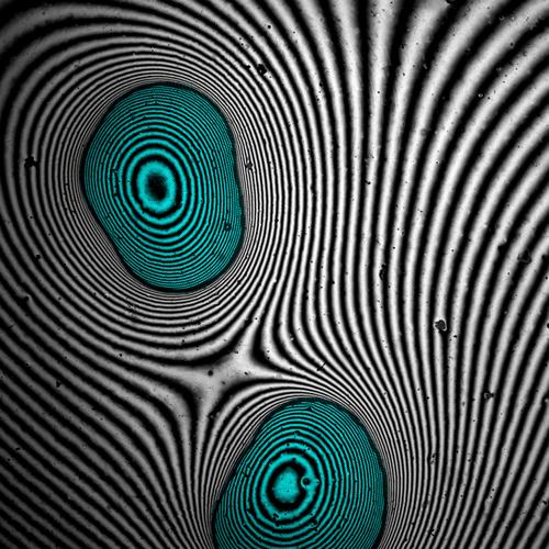
People’s Second Place: Bridging the gap. Credit: Jason Wexler (graduate student) and Howard A. Stone (faculty) Department of Mechanical and Aerospace Engineering When drops of liquid are trapped in a thin gap between two solids, a strong negative pressure develops inside the drops. If the solids are flexible, this pressure deforms the solids to close the gap. In our experiment the solids are transparent, which allows us to image the drops from above. Alternating dark and light lines represent lines of constant gap height, much like the lines on a topological map. These lines are caused by light interference, which is the phenomenon responsible for the beautiful rainbow pattern in an oil slick. The blue areas denote the extent of the drops. Since the drops pull the gap closed, the areas of minimum gap height (i.e. maximum deformation) are inside the drops, at the center of the concentric rings.
The Princeton University Art of Science 2013 exhibit can now be viewed in a new online gallery. The exhibit consists of 43 images of artistic merit created during the course of scientific research:
The gallery features the top three awards in a juried competition as well as the top three “People’s Choice” images.
The physical Art of Science 2013 gallery opened May 10 with a reception attended by about 200 people in the Friend Center on the Princeton University campus. The works were chosen from 170 images submitted from 24 different departments across campus.
“Like art, science and engineering are deeply creative activities,” said Pablo Debenedetti, the recently appointed Dean for Research at Princeton who served as master of ceremonies at the opening reception. “Also like art, science and engineering at their very best are highly unpredictable in their outcomes. The Art of Science exhibit celebrates the beauty of unpredictability and the unpredictability of beauty.” [emphasis mine]
Adam Finkelstein, professor of computer science and one of the exhibit organizers, said that Art of Science spurs debate among artists about the nature of art while opening scientists to new ways of “seeing” their own research. “At the same time,” Finkelstein said, “this striking imagery serves as a democratic window through which non-experts can appreciate the thrill of scientific discovery.”
The top three entrants as chosen by a distinguished jury received cash prizes in amounts calculated by the golden ratio (whose proportions have since antiquity been considered to be aesthetically pleasing): first prize, $250; second prize, $154.51; and third prize, $95.49. [emphasis mine]
…
The physical exhibit is located in the Friend Center on the Princeton University campus in Princeton, N.J.. The exhibit is free and open to the public, Monday through Friday, from 9 a.m. to 6 p.m.
There are three pages of viewing delight at Princeton’s Art of Science 2013 online gallery. Have a lovely weekend picking your favourites.
There’s such a thing as too much information and not enough knowledge, a condition I’m currently suffering from with regard to artificial photosynthesis. Before expanding on that theme, here’s the latest about artificial photosynthesis from a May 16, 2013 Lawrence Berkeley National Laboratory news release (also available on EurekAlert),
In the wake of the sobering news that atmospheric carbon dioxide is now at its highest level in at least three million years, an important advance in the race to develop carbon-neutral renewable energy sources has been achieved. Scientists with the U.S. Department of Energy (DOE)’s Lawrence Berkeley National Laboratory (Berkeley Lab) have reported the first fully integrated nanosystem for artificial photosynthesis. While “artificial leaf” is the popular term for such a system, the key to this success was an “artificial forest.”
Here’s a more detailed description of the system, from the news release,
“Similar to the chloroplasts in green plants that carry out photosynthesis, our artificial photosynthetic system is composed of two semiconductor light absorbers, an interfacial layer for charge transport, and spatially separated co-catalysts,” says Peidong Yang, a chemist with Berkeley Lab’s Materials Sciences Division, who led this research. “To facilitate solar water- splitting in our system, we synthesized tree-like nanowire heterostructures, consisting of silicon trunks and titanium oxide branches. Visually, arrays of these nanostructures very much resemble an artificial forest.”
…
… Artificial photosynthesis, in which solar energy is directly converted into chemical fuels, is regarded as one of the most promising of solar technologies. A major challenge for artificial photosynthesis is to produce hydrogen cheaply enough to compete with fossil fuels. Meeting this challenge requires an integrated system that can efficiently absorb sunlight and produce charge-carriers to drive separate water reduction and oxidation half-reactions.
More specifically,
“In natural photosynthesis the energy of absorbed sunlight produces energized charge-carriers that execute chemical reactions in separate regions of the chloroplast,” Yang says. “We’ve integrated our nanowire nanoscale heterostructure into a functional system that mimics the integration in chloroplasts and provides a conceptual blueprint for better solar-to-fuel conversion efficiencies in the future.”
When sunlight is absorbed by pigment molecules in a chloroplast, an energized electron is generated that moves from molecule to molecule through a transport chain until ultimately it drives the conversion of carbon dioxide into carbohydrate sugars. This electron transport chain is called a “Z-scheme” because the pattern of movement resembles the letter Z on its side. Yang and his colleagues also use a Z-scheme in their system only they deploy two Earth abundant and stable semiconductors – silicon and titanium oxide – loaded with co-catalysts and with an ohmic contact inserted between them. Silicon was used for the hydrogen-generating photocathode and titanium oxide for the oxygen-generating photoanode. The tree-like architecture was used to maximize the system’s performance. Like trees in a real forest, the dense arrays of artificial nanowire trees suppress sunlight reflection and provide more surface area for fuel producing reactions.
“Upon illumination photo-excited electron−hole pairs are generated in silicon and titanium oxide, which absorb different regions of the solar spectrum,” Yang says. “The photo-generated electrons in the silicon nanowires migrate to the surface and reduce protons to generate hydrogen while the photo-generated holes in the titanium oxide nanowires oxidize water to evolve oxygen molecules. The majority charge carriers from both semiconductors recombine at the ohmic contact, completing the relay of the Z-scheme, similar to that of natural photosynthesis.”
Under simulated sunlight, this integrated nanowire-based artificial photosynthesis system achieved a 0.12-percent solar-to-fuel conversion efficiency. Although comparable to some natural photosynthetic conversion efficiencies, this rate will have to be substantially improved for commercial use. [emphasis mine] However, the modular design of this system allows for newly discovered individual components to be readily incorporated to improve its performance. For example, Yang notes that the photocurrent output from the system’s silicon cathodes and titanium oxide anodes do not match, and that the lower photocurrent output from the anodes is limiting the system’s overall performance.
“We have some good ideas to develop stable photoanodes with better performance than titanium oxide,” Yang says. “We’re confident that we will be able to replace titanium oxide anodes in the near future and push the energy conversion efficiency up into single digit percentages.”
Now I can discuss my confusion, which stems from my May 24, 2013 posting about work done at the Argonne National Laboratory,
… Researchers still have a long way to go before they will be able to create devices that match the light harvesting efficiency of a plant.
One reason for this shortcoming, Tiede [Argonne biochemist David Tiede] explained, is that artificial photosynthesis experiments have not been able to replicate the molecular matrix that contains the chromophores. “The level that we are at with artificial photosynthesis is that we can make the pigments and stick them together, but we cannot duplicate any of the external environment,” he said. “The next step is to build in this framework, and then these kinds of quantum effects may become more apparent.”
Because the moment when the quantum effect occurs is so short-lived – less than a trillionth of a second – scientists will have a hard time ascertaining biological and physical rationales for their existence in the first place. [emphasis mine]
It’s not clear to me whether or not the folks at the Berkeley Lab bypassed the ‘problem’ described by Tiede or solved it to achieve solar-to-fuel conversion rates comparable to natural photosynthesis conversions. As I noted, too much information/not enough knowledge.
“Spring is like a perhaps hand,” wrote the poet E. E. Cummings: “carefully / moving a perhaps / fraction of flower here placing / an inch of air there… / without breaking anything.”
This was written to celebrate the publication of a paper by Wim L. Noorduin and others, from the press release (Note: Links have been removed),
By simply manipulating chemical gradients in a beaker of fluid, Wim L. Noorduin, a postdoctoral fellow at the Harvard School of Engineering and Applied Sciences (SEAS) and lead author of a paper appearing on the cover of the May 17 issue of Science, has found that he can control the growth behavior of these crystals to create precisely tailored structures.
“For at least 200 years, people have been intrigued by how complex shapes could have evolved in nature. This work helps to demonstrate what’s possible just through environmental, chemical changes,” says Noorduin.
The precipitation of the crystals depends on a reaction of compounds that are diffusing through a liquid solution. The crystals grow toward or away from certain chemical gradients as the pH of the reaction shifts back and forth. The conditions of the reaction dictate whether the structure resembles broad, radiating leaves, a thin stem, or a rosette of petals.
…
Replicating this type of effect in the laboratory was a matter of identifying a suitable chemical reaction and testing, again and again, how variables like the pH, temperature, and exposure to air might affect the nanoscale structures.
The project fits right in with the work of Joanna Aizenberg, an expert in biologically inspired materials science, biomineralization, and self-assembly, and principal investigator for this research.
Aizenberg is the Amy Smith Berylson Professor of Materials Science at Harvard SEAS, Professor of Chemistry and Chemical Biology in the Harvard Department of Chemistry and Chemical Biology, and a Core Faculty Member of the Wyss Institute for Biologically Inspired Engineering at Harvard.
Here are some details about how the scientists created their ‘flowers, from the press release,
To create the flower structures, Noorduin and his colleagues dissolve barium chloride (a salt) and sodium silicate (also known as waterglass) into a beaker of water. Carbon dioxide from air naturally dissolves in the water, setting off a reaction which precipitates barium carbonate crystals. As a byproduct, it also lowers the pH of the solution immediately surrounding the crystals, which then triggers a reaction with the dissolved waterglass. This second reaction adds a layer of silica to the growing structures, uses up the acid from the solution, and allows the formation of barium carbonate crystals to continue.
“You can really collaborate with the self-assembly process,” says Noorduin. “The precipitation happens spontaneously, but if you want to change something then you can just manipulate the conditions of the reaction and sculpt the forms while they’re growing.”
Increasing the concentration of carbon dioxide, for instance, helps to create ‘broad-leafed’ structures. Reversing the pH gradient at the right moment can create curved, ruffled structures.
Noorduin and his colleagues have grown the crystals on glass slides and metal blades; they’ve even grown a field of flowers in front of President Lincoln’s seat on a one-cent coin.
“When you look through the electron microscope, it really feels a bit like you’re diving in the ocean, seeing huge fields of coral and sponges,” describes Noorduin. “Sometimes I forget to take images because it’s so nice to explore.”
Scientists try to understand how to initiate and control the growth of nanomaterials and are exploring different ways to design and build up nanostructures with fine control over shapes. In nature, many organic forms grow bilaterally, that is, symmetrically in two distinct directions. An international team of researchers from the University of Vienna (Austria), the University of Surrey (UK) and the IFW Dresden (Germany) have now achieved such a bilateral formation of inorganic nanomaterials in a controlled environment by implementing a new method.
The scientists pressurized a gas consisting of carbon and iron atoms at an elevated temperature until they observed two arms of carbon atoms spontaneously started growing out of an iron core. When the iron core was small enough, the two carbon arms started spiraling at their ends so that the whole nanostructure bore a striking resemblance with a twirled moustache. [emphasis mine] “The encouraging insights we gained from our experiments provide a very good starting point for the controlled production of extraordinary new materials with designed nanostructures”, expects Dr. Hidetsugu Shiozawa, leading author of the scientific publication and researcher at the Faculty of Physics at the University of Vienna.
I’ll get back to the twirled moustache in a moment. In the meantime, here’s a citation for and a link to the researchers’ paper,
The paper is open access, which means finding this illustration (the one I think shows the twirling most clearly) was easy,
Figure 2: Spiralling and kinked bicones produced by a hodographic method using parameters (Δϕ, Δθ, and ΔTi) as a function of the cone length. [downloaded from http://www.nature.com/srep/2013/130514/srep01840/full/srep01840.html]
I believe the imagery associated with twirling moustaches, i.e., the villain in a silent movie cackling and twirling his moustaches as he watches over the heroine he’s tied the train tracks await the steaming train headed their way, is well known. Apparently, the trope was not as popular as most of us imagine. I found a fabulous website, The Bioscope; Formerly reporting on the world of early and silent cinema, which tells all in a Nov. 25, 2010 essay,
It’s a mocking idea of a silent film, the kind of silent film that was never made. All those know [who?] don’t know silent films know one thing about them – that they featured evil villains who twirled their moustaches then tied a hapless female to the railway track. And all those who do know silent films know that such scenes were hackneyed even before films were invented, and the few films that did show them did so as parody.
It’s an issue that comes up time and time again, so let’s try and pin down the historical truth. The idea of an entertainment where someone is tied to a railway track and is rescued in the nick of time certainly predates cinema. The entertainment that put the idea into the popular imagination was an 1867 stage melodrama written by American playwright and theatre manager Augustin Daly entitled Under the Gaslight which featured a man tried to railway tracks who was rescued by a woman before he could be run over by the oncoming train (Victorian theatre revelled in such stage spectaculars).
There’s lots more to the essay along with some great stills and this very charming video animation that manages to poke fun at the trope and the modern UK rail system,
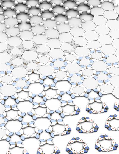
Writing in Nature, a large international team led Dr Roman Gorbachev from The University of Manchester shows that, when graphene placed on top of insulating boron nitride, or ‘white graphene’, the electronic properties of graphene change dramatically revealing a pattern resembling a butterfly.
The pattern is referred to as the elusive Hofstadter butterfly that has been known in theory for many decades but never before observed in experiments.
More of the science needs to be explained before moving on with the ‘butterflies’ (from the news release),
One of the most remarkable properties of graphene is its high conductivity – thousands of times higher than copper. This is due to a very special pattern created by electrons that carry electricity in graphene. The carriers are called Dirac fermions and mimic massless relativistic particles called neutrinos, studies of which usually require huge facilities such as at CERN. The possibility to address similar physics in a desk-top experiment is one of the most renowned features of graphene.
Now the Manchester scientists have found a way to create multiple clones of Dirac fermions. Graphene is placed on top of boron nitride so that graphene’s electrons can ‘feel’ individual boron and nitrogen atoms. Moving along this atomic ‘washboard’, electrons rearrange themselves once again producing multiple copies of the original Dirac fermions.
Here’s where the butterflies appear (from the news release),
The researchers can create even more clones by applying a magnetic field. The clones produce an intricate pattern; the Hofstadter butterfly. It was first predicted by mathematician Douglas Hofstadter in 1976 and, despite many dedicated experimental efforts, no more than a blurred glimpse was reported before.
In addition to the described fundamental interest, the Manchester study proves that it is possible to modify properties of atomically-thin materials by placing them on top of each other. This can be useful, for example, for graphene applications such as ultra-fast photodetectors and transistors, providing a way to tweak its incredible properties.
Coincidentally, another team has also observed the Hofstadter butterfly on a graphene substrate. From the May 16, 2013 news item on Azonano,
Two research teams at the National High Magnetic Field Laboratory (MagLab) broke through a nearly 40-year barrier recently when they observed a never-before-seen energy pattern.
…
“The observation of the ‘Hofstadter butterfly’ marks a real landmark in condensed matter physics and high magnetic field research,” said Greg Boebinger, director of the MagLab. “It opens a new experimental direction in materials research.”
This groundbreaking research demanded the ability to measure samples of materials at very low temperatures and very high magnetic fields, up to 35 tesla. Both of those conditions are available at the MagLab, making it an international destination for scientific exploration.
The unique periodic structure used to observe the butterfly pattern was composed of boron nitride (BN) and graphene.
One research team was led by Columbia University’s Philip Kim and included researchers from City University of New York, the University of Central Florida, Tohoku University and the National Institute for Materials Science in Japan. The team’s work will be published today in the Advanced Online Publication of the journal Nature. Similar results were discovered at the MagLab by a group led by Pablo Jarillo-Herrero and Raymond Ashoori at MIT, as well as scientists from Tohoku University and the National Institute for Materials Science in Japan. Their work is expected to be published soon.
For those who just can’t get enough graphene butterflies here are citations for and links to both recently published papers (the Jarillo-Herrero/Ashoori team will be publishing their work soon).
Cloning of Dirac fermions in graphene superlattices by L. A. Ponomarenko, R. V. Gorbachev, G. L. Yu,D. C. Elias, R. Jalil, A. A. Patel, A. Mishchenko, A. S. Mayorov, C. R. Woods, J. R. Wallbank, M. Mucha-Kruczynski, B. A. Piot, M. Potemski, I. V. Grigorieva, K. S. Novoselov, F. Guinea, V. I. Fal’ko & A. K. Geim. Nature doi:10.1038/nature12187 Published online
![Figure 2: Spiralling and kinked bicones produced by a hodographic method using parameters (Δϕ, Δθ, and ΔTi) as a function of the cone length. [downloaded from http://www.nature.com/srep/2013/130514/srep01840/full/srep01840.html]](http://www.frogheart.ca/wp-content/uploads/2013/05/TwirlingCarbon.jpg)