Tag Archives: electronic synapses

Nano-neurons from a French-Japanese-US research team

This news about nano-neurons comes from a Nov. 8, 2017 news item on defenceweb.co.za,

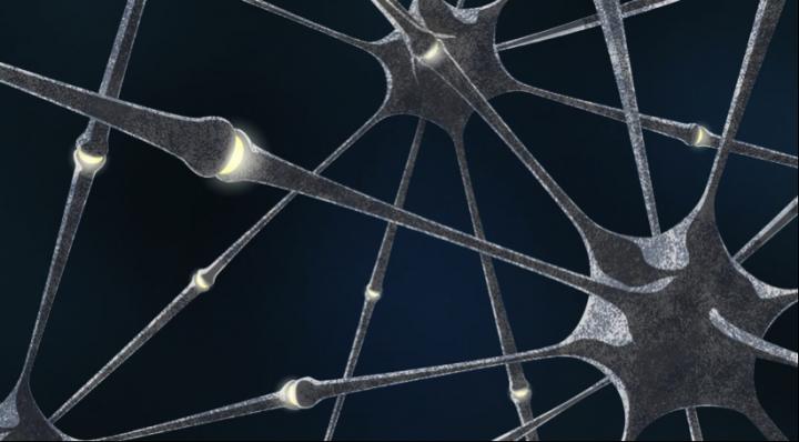
Researchers from the Joint Physics Unit CNRS/Thales, the Nanosciences and Nanotechnologies Centre (CNRS/Université Paris Sud), in collaboration with American and Japanese researchers, have developed the world’s first artificial nano-neuron with the ability to recognise numbers spoken by different individuals. Just like the recent development of electronic synapses described in a Nature article, this electronic nano-neuron is a breakthrough in artificial intelligence and its potential applications.

A Sept. 19, 2017 Thales press release, which originated the news item, expands on the theme,

The latest artificial intelligence algorithms are able to recognise visual and vocal cues with high levels of performance. But running these programs on conventional computers uses 10,000 times more energy than the human brain. To reduce electricity consumption, a new type of computer is needed. It is inspired by the human brain and comprises vast numbers of miniaturised neurons and synapses. Until now, however, it had not been possible to produce a stable enough artificial nano-neuron which would process the information reliably.

Today [Sept. 19, 2017 or July 27, 2017 when the paper was published in Nature?]], for the first time, researchers have developed a nano-neuron with the ability to recognise numbers spoken by different individuals with 99.6% accuracy. This breakthrough relied on the use of an exceptionally stable magnetic oscillator. Each gyration of this nano-compass generates an electrical output, which effectively imitates the electrical impulses produced by biological neurons. In the next few years, these magnetic nano-neurons could be interconnected via artificial synapses, such as those recently developed, for real-time big data analytics and classification.

The project is a collaborative initiative between fundamental research laboratories and applied research partners. The long-term goal is to produce extremely energy-efficient miniaturised chips with the intelligence needed to learn from and adapt to the constantly ever-changing and ambiguous situations of the real world. These electronic chips will have many practical applications, such as providing smart guidance to robots or autonomous vehicles, helping doctors in their diagnosis’ and improving medical prostheses. This project included researchers from the Joint Physics Unit CNRS/Thales, the AIST, the CNS-NIST, and the Nanosciences and Nanotechnologies Centre (CNRS/Université Paris-Sud).

About the CNRS
The French National Centre for Scientific Research is Europe’s largest public research institution. It produces knowledge for the benefit of society. With nearly 32,000 employees, a budget exceeding 3.2 billion euros in 2016, and offices throughout France, the CNRS is present in all scientific fields through its 1100 laboratories. With 21 Nobel laureates and 12 Fields Medal winners, the organization has a long tradition of excellence. It carries out research in mathematics, physics, information sciences and technologies, nuclear and particle physics, Earth sciences and astronomy, chemistry, biological sciences, the humanities and social sciences, engineering and the environment.

About the Université Paris-Saclay (France)
To meet global demand for higher education, research and innovation, 19 of France’s most renowned establishments have joined together to form the Université Paris-Saclay. The new university provides world-class teaching and research opportunities, from undergraduate courses to graduate schools and doctoral programmes, across most disciplines including life and natural sciences as well as social sciences. With 9,000 masters students, 5,500 doctoral candidates, an equivalent number of engineering students and an extensive undergraduate population, some 65,000 people now study at member establishments.

About the Center for Nanoscale Science & Technology (Maryland, USA)
The CNST is a national user facility purposely designed to accelerate innovation in nanotechnology-based commerce. Its mission is to operate a national, shared resource for nanoscale fabrication and measurement and develop innovative nanoscale measurement and fabrication capabilities to support researchers from industry, academia, NIST and other government agencies in advancing nanoscale technology from discovery to production. The Center, located in the Advanced Measurement Laboratory Complex on NIST’s Gaithersburg, MD campus, disseminates new nanoscale measurement methods by incorporating them into facility operations, collaborating and partnering with others and providing international leadership in nanotechnology.

About the National Institute of Advanced Industrial Science and Technology (Japan)
The National Institute of Advanced Industrial Science and Technology (AIST), one of the largest public research institutes in Japan, focuses on the creation and practical realization of technologies useful to Japanese industry and society, and on bridging the gap between innovative technological seeds and commercialization. For this, AIST is organized into 7 domains (Energy and Environment, Life Science and Biotechnology, Information Technology and Human Factors, Materials and Chemistry, Electronics and Manufacturing, Geological

About the Centre for Nanoscience and Nanotechnology (France)
Established on 1 June 2016, the Centre for Nanosciences and Nanotechnologies (C2N) was launched in the wake of the joint CNRS and Université Paris-Sud decision to merge and gather on the same campus site the Laboratory for Photonics and Nanostructures (LPN) and the Institut d’Electronique Fondamentale (IEF). Its location in the École Polytechnique district of the Paris-Saclay campus will be completed in 2017 while the new C2N buildings are under construction. The centre conducts research in material science, nanophotonics, nanoelectronics, nanobiotechnologies and microsystems, as well as in nanotechnologies.

There is a video featuring researcher Julie Grollier discussing their work but you will need your French language skills,

(If you’re interested, there is an English language video published on youtube on Feb. 19, 2017 with Julie Grollier speaking more generally about the field at the World Economic Forum about neuromorphic computing,  https://www.youtube.com/watch?v=Sm2BGkTYFeQ

Here’s a link to and a citation for the team’s July 2017 paper,

Neuromorphic computing with nanoscale spintronic oscillators by Jacob Torrejon, Mathieu Riou, Flavio Abreu Araujo, Sumito Tsunegi, Guru Khalsa, Damien Querlioz, Paolo Bortolotti, Vincent Cros, Kay Yakushiji, Akio Fukushima, Hitoshi Kubota, Shinji Yuasa, Mark D. Stiles, & Julie Grollier. Nature 547, 428–431 (27 July 2017) doi:10.1038/nature23011 Published online 26 July 2017

This paper is behind a paywall.

Memristor-based electronic synapses for neural networks

Caption: Neuron connections in biological neural networks. Credit: MIPT press office

Caption: Neuron connections in biological neural networks. Credit: MIPT press office

Russian scientists have recently published a paper about neural networks and electronic synapses based on ‘thin film’ memristors according to an April 19, 2016 news item on Nanowerk,

A team of scientists from the Moscow Institute of Physics and Technology (MIPT) have created prototypes of “electronic synapses” based on ultra-thin films of hafnium oxide (HfO2). These prototypes could potentially be used in fundamentally new computing systems.

An April 20, 2016 MIPT press release (also on EurekAlert), which originated the news item (the date inconsistency likely due to timezone differences) explains the connection between thin films and memristors,

The group of researchers from MIPT have made HfO2-based memristors measuring just 40×40 nm2. The nanostructures they built exhibit properties similar to biological synapses. Using newly developed technology, the memristors were integrated in matrices: in the future this technology may be used to design computers that function similar to biological neural networks.

Memristors (resistors with memory) are devices that are able to change their state (conductivity) depending on the charge passing through them, and they therefore have a memory of their “history”. In this study, the scientists used devices based on thin-film hafnium oxide, a material that is already used in the production of modern processors. This means that this new lab technology could, if required, easily be used in industrial processes.

“In a simpler version, memristors are promising binary non-volatile memory cells, in which information is written by switching the electric resistance – from high to low and back again. What we are trying to demonstrate are much more complex functions of memristors – that they behave similar to biological synapses,” said Yury Matveyev, the corresponding author of the paper, and senior researcher of MIPT’s Laboratory of Functional Materials and Devices for Nanoelectronics, commenting on the study.

The press release offers a description of biological synapses and their relationship to learning and memory,

A synapse is point of connection between neurons, the main function of which is to transmit a signal (a spike – a particular type of signal, see fig. 2) from one neuron to another. Each neuron may have thousands of synapses, i.e. connect with a large number of other neurons. This means that information can be processed in parallel, rather than sequentially (as in modern computers). This is the reason why “living” neural networks are so immensely effective both in terms of speed and energy consumption in solving large range of tasks, such as image / voice recognition, etc.

Over time, synapses may change their “weight”, i.e. their ability to transmit a signal. This property is believed to be the key to understanding the learning and memory functions of thebrain.

From the physical point of view, synaptic “memory” and “learning” in the brain can be interpreted as follows: the neural connection possesses a certain “conductivity”, which is determined by the previous “history” of signals that have passed through the connection. If a synapse transmits a signal from one neuron to another, we can say that it has high “conductivity”, and if it does not, we say it has low “conductivity”. However, synapses do not simply function in on/off mode; they can have any intermediate “weight” (intermediate conductivity value). Accordingly, if we want to simulate them using certain devices, these devices will also have to have analogous characteristics.

The researchers have provided an illustration of a biological synapse,

Fig.2 The type of electrical signal transmitted by neurons (a “spike”). The red lines are various other biological signals, the black line is the averaged signal. Source: MIPT press office

Fig.2 The type of electrical signal transmitted by neurons (a “spike”). The red lines are various other biological signals, the black line is the averaged signal. Source: MIPT press office

Now, the press release ties the memristor information together with the biological synapse information to describe the new work at the MIPT,

As in a biological synapse, the value of the electrical conductivity of a memristor is the result of its previous “life” – from the moment it was made.

There is a number of physical effects that can be exploited to design memristors. In this study, the authors used devices based on ultrathin-film hafnium oxide, which exhibit the effect of soft (reversible) electrical breakdown under an applied external electric field. Most often, these devices use only two different states encoding logic zero and one. However, in order to simulate biological synapses, a continuous spectrum of conductivities had to be used in the devices.

“The detailed physical mechanism behind the function of the memristors in question is still debated. However, the qualitative model is as follows: in the metal–ultrathin oxide–metal structure, charged point defects, such as vacancies of oxygen atoms, are formed and move around in the oxide layer when exposed to an electric field. It is these defects that are responsible for the reversible change in the conductivity of the oxide layer,” says the co-author of the paper and researcher of MIPT’s Laboratory of Functional Materials and Devices for Nanoelectronics, Sergey Zakharchenko.

The authors used the newly developed “analogue” memristors to model various learning mechanisms (“plasticity”) of biological synapses. In particular, this involved functions such as long-term potentiation (LTP) or long-term depression (LTD) of a connection between two neurons. It is generally accepted that these functions are the underlying mechanisms of  memory in the brain.

The authors also succeeded in demonstrating a more complex mechanism – spike-timing-dependent plasticity, i.e. the dependence of the value of the connection between neurons on the relative time taken for them to be “triggered”. It had previously been shown that this mechanism is responsible for associative learning – the ability of the brain to find connections between different events.

To demonstrate this function in their memristor devices, the authors purposefully used an electric signal which reproduced, as far as possible, the signals in living neurons, and they obtained a dependency very similar to those observed in living synapses (see fig. 3).

Fig.3. The change in conductivity of memristors depending on the temporal separation between "spikes"(rigth) and thr change in potential of the neuron connections in biological neural networks. Source: MIPT press office

Fig.3. The change in conductivity of memristors depending on the temporal separation between “spikes”(rigth) and thr change in potential of the neuron connections in biological neural networks. Source: MIPT press office

These results allowed the authors to confirm that the elements that they had developed could be considered a prototype of the “electronic synapse”, which could be used as a basis for the hardware implementation of artificial neural networks.

“We have created a baseline matrix of nanoscale memristors demonstrating the properties of biological synapses. Thanks to this research, we are now one step closer to building an artificial neural network. It may only be the very simplest of networks, but it is nevertheless a hardware prototype,” said the head of MIPT’s Laboratory of Functional Materials and Devices for Nanoelectronics, Andrey Zenkevich.

Here’s a link to and a citation for the paper,

Crossbar Nanoscale HfO2-Based Electronic Synapses by Yury Matveyev, Roman Kirtaev, Alena Fetisova, Sergey Zakharchenko, Dmitry Negrov and Andrey Zenkevich. Nanoscale Research Letters201611:147 DOI: 10.1186/s11671-016-1360-6

Published: 15 March 2016

This is an open access paper.