Tag Archives: University of Oxford

Music on the web, a spider’s web, that is

I was expecting to see Markus Buehler and MIT (Massachusetts Institute of Technology) mentioned in this latest work on spiderwebs and music. Surprise! This latest research is from three universities in the UK as per a June 3, 2014 news item on ScienceDaily,

Spider silk transmits vibrations across a wide range of frequencies so that, when plucked like a guitar string, its sound carries information about prey, mates, and even the structural integrity of a web.

The discovery was made by researchers from the Universities of Oxford, Strathclyde, and Sheffield who fired bullets and lasers at spider silk to study how it vibrates. They found that, uniquely, when compared to other materials, spider silk can be tuned to a wide range of harmonics. The findings, to be reported in the journal Advanced Materials, not only reveal more about spiders but could also inspire a wide range of new technologies, such as tiny light-weight sensors.

A June 3, 2014 University of Oxford news release (also on EurekAlert), which originated the news item, explains the research and describes how it was conducted (firing bullets?),

‘Most spiders have poor eyesight and rely almost exclusively on the vibration of the silk in their web for sensory information,’ said Beth Mortimer of the Oxford Silk Group at Oxford University, who led the research. ‘The sound of silk can tell them what type of meal is entangled in their net and about the intentions and quality of a prospective mate. By plucking the silk like a guitar string and listening to the ‘echoes’ the spider can also assess the condition of its web.’

‘Most spiders have poor eyesight and rely almost exclusively on the vibration of the silk in their web for sensory information,’ said Beth Mortimer of the Oxford Silk Group at Oxford University, who led the research. ‘The sound of silk can tell them what type of meal is entangled in their net and about the intentions and quality of a prospective mate. By plucking the silk like a guitar string and listening to the ‘echoes’ the spider can also assess the condition of its web.’

This quality is used by the spider in its web by ‘tuning’ the silk: controlling and adjusting both the inherent properties of the silk, and the tensions and interconnectivities of the silk threads that make up the web. To study the sonic properties of the spider’s gossamer threads the researchers used ultra-high-speed cameras to film the threads as they responded to the impact of bullets. [emphasis mine] In addition, lasers were used to make detailed measurements of even the smallest vibration.

‘The fact that spiders can receive these nanometre vibrations with organs on each of their legs, called slit sensillae, really exemplifies the impact of our research about silk properties found in our study,’ said Dr Shira Gordon of the University of Strathclyde, an author involved in this research.

‘These findings further demonstrate the outstanding properties of many spider silks that are able to combine exceptional toughness with the ability to transfer delicate information,’ said Professor Fritz Vollrath of the Oxford Silk Group at Oxford University, an author of the paper. ‘These are traits that would be very useful in light-weight engineering and might lead to novel, built-in ‘intelligent’ sensors and actuators.’

Dr Chris Holland of the University of Sheffield, an author of the paper, said: ‘Spider silks are well known for their impressive mechanical properties, but the vibrational properties have been relatively overlooked and now we find that they are also an awesome communication tool. Yet again spiders continue to impress us in more ways than we can imagine.’

Beth Mortimer said: ‘It may even be that spiders set out to make a web that ‘sounds right’ as its sonic properties are intimately related to factors such as strength and flexibility.’

The research paper has not yet been published in Advanced Materials (I checked this morning, June 4, 2014).

However, there is this video from the researchers,

As for Markus Buehler’s work at MIT, you can find out more in my Nov. 28, 2012 posting, Producing stronger silk musically.

Isis Innovation (University of Oxford, UK) spins out buckyball company, Designer Carbon Materials

Buckyballs are also known as Buckminsterfullerenes. The name is derived from Buckminster Fuller who designed something he called geodesic domes, from the Wikipedia entry (Note: Links have been removed),

Buckminsterfullerene (or bucky-ball) is a spherical fullerene molecule with the formula C60 [C = carbon; 60 is the number of carbon atoms in the molecule]. It has a cage-like fused-ring structure (truncated icosahedron) which resembles a soccer ball, made of twenty hexagons and twelve pentagons, with a carbon atom at each vertex of each polygon and a bond along each polygon edge.

It was first generated in 1985 by Harold Kroto, James R. Heath, Sean O’Brien, Robert Curl, and Richard Smalley at Rice University.[2] Kroto, Curl and Smalley were awarded the 1996 Nobel Prize in Chemistry for their roles in the discovery of buckminsterfullerene and the related class of molecules, the fullerenes. The name is a reference to Buckminster Fuller, as C60 resembles his trademark geodesic domes. Buckminsterfullerene is the most commonly naturally occurring fullerene molecule, as it can be found in small quantities in soot.[3][4] Solid and gaseous forms of the molecule have been detected in deep space.[5]

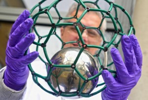
Here’s a model of a buckyball,

Courtesy: Isis Innovation (Oxford University)

Courtesy: Isis Innovation (Oxford University)

An April 15, 2014 University of Oxford (Isis Innovation) news release (h/t phys.org) describes the news research and some technical details while avoiding any mention of how they’ve tackled the production problems (a major issue, which has seriously constrained their commercial use),

The firm, Designer Carbon Materials, has been established by Isis Innovation, the University of Oxford’s technology commercialisation company, and will cost-effectively manufacture commercially useful quantities of the spherical carbon cage structures. Designer Carbon Materials is based on research from Dr Kyriakos Porfyrakis of Oxford University’s Department of Materials.

‘It is possible to insert a variety of useful atoms or atomic clusters into the hollow interior of these ball-like molecules, giving them new and intriguing abilities. Designer Carbon Materials will focus on the production of these value-added materials for a range of applications,’ said Dr Porfyrakis.

‘For instance, fullerenes are currently used as electron acceptors in polymer-based solar cells achieving some of the highest power conversion efficiencies known for these kinds of solar cells. Our endohedral fullerenes are even better electron-acceptors and therefore have the potential to lead to efficiencies exceeding 10 per cent.

‘The materials could also be developed as superior MRI contrast agents for medical imaging and as diagnostics for Alzheimer’s and Parkinson’s, as they are able to detect the presence of superoxide free radical molecules which may cause these conditions. We are receiving fantastic interest from organisations developing these applications, who until now have been unable to access useful quantities of these materials.’

The manufacturing process, patented by Isis Innovation, will continue to be developed by Designer Carbon Materials as it also makes its first sales of these extremely high-value materials.

Tom Hockaday, managing director of Isis Innovation, said: ‘This is a great example of an Isis spin-out which is both looking at exciting future applications for its technology and also answering a real market need. There is already significant demand for these nanomaterials and we expect the first customer orders will be fulfilled over the next few months.’

Investment in the company has been led by Oxford Technology Management and the Oxford Invention Fund. Lucius Carey from Oxford Technology Management said: ‘We are delighted to be investing in Designer Carbon Materials. The purposes of the investment will be to move into commercial premises and to scale up.’

Isis Innovation is a University of Oxford initiative and you can find out more about Isis Innovation here. As for the new spin-out company, Designer Carbon Materials, they have no website that I’ve been able to find but there is this webpage on the Isis Innovation website.

Oxford’s 2014 Nanotechnology Summer School

Here’s some information about Oxford’s sixth annual nanotechnology summer programme from a March 25, 2014 news item on Nanowerk (Note: A link has been removed),

The theme of the sixth annual Oxford Nanotechnology Summer School in 2014 will be ‘An Introduction to Bionanotechnology’.

Each year Oxford’s Nanotechnology Summer School focuses on applications of nanotechnologies in a different field. Comprising presentations from leading researchers and practitioners from the University of Oxford and beyond, the Nanotechnology Summer School is essential for anyone with an interest in these topics.

There’s more about the summer school on the University of Oxford’s Nanotechnology Summer School 2014’s course page,

This five-day intensive course provides a thorough introduction to the exciting and emerging field of bionanotechnology. Each of the five days of the Nanotechnology Summer School has a dedicated theme and is led by key researchers in the field. The course will be valuable to those seeking an introduction to current research and applications in the subject.

The first day of the Summer School gives an introduction to cell biology and bionanotechnology. The following four days focus on bioanalytical techniques; applied genomics and proteomics; nanoparticles, nanostructures and biomimetics; and the interaction of nanomaterials with biological systems, respectively.

The full Summer School programme will be as follows:

For those who like to know about the costs and attendance options (from the course page),

Payment

Summer School fees include electronic course materials, tuition, refreshments and three-course lunches. The price does not include accommodation. All courses are VAT exempt. There may also be some social events on certain days of the Summer School.

Student discounts

We offer a discounted fee to students in higher education. The student fee rate for five days of the Nanotechnology Summer School is £680.00. It is not possible to enrol online if you wish to take the course at a discounted rate. To apply at the discounted rate, please contact us for details: email nano@conted.ox.ac.uk.

Alumni Card-holders discount

Alumni Card-holders benefit from a 10% discount* on the Nanotechnology Summer School. If you wish to enrol, please remember to quote the code given in e-Pidge to ensure you receive your discount.

* This offer is subject to availability, cannot be used retrospectively or in conjunction with any other offers or concessions available from either the University of Oxford or the Department for Continuing Education.

Fee options

Programme Fee
Five Days – Standard Fee: £1340.00
Five Days – Student Fee: £680.00
One Day – Standard Rate: £295.00
One Day – Student Rate: £150.00

Here’s how you can apply,

Please note that we cannot accept applications from those who are under 18 years of age.

You can apply for this course in the following ways:

Apply online
enrol onlineto secure your place on this course now
Apply by post, email or fax
PDF application form PDF document.

Terms and Conditions (important: please read before applying) .
Guidance Notes (important: please read before applying) PDF document.

Good luck1

Finding a successor to graphene

The folks at the Lawrence Berkeley National Laboratory (Berkeley Lab) have announced a ‘natural’ 3D counterpart of graphene in a Jan. 16, 2014 Berkeley Lab news release (also on EurekAlert and on Azonano dated Jan. 17, 2014),

The discovery of what is essentially a 3D version of graphene – the 2D sheets of carbon through which electrons race at many times the speed at which they move through silicon – promises exciting new things to come for the high-tech industry, including much faster transistors and far more compact hard drives. A collaboration of researchers at the U.S Department of Energy (DOE)’s Lawrence Berkeley National Laboratory (Berkeley Lab) has discovered that sodium bismuthate can exist as a form of quantum matter called a three-dimensional topological Dirac semi-metal (3DTDS). This is the first experimental confirmation of 3D Dirac fermions in the interior or bulk of a material, a novel state that was only recently proposed by theorists.

The news release provides a description of graphene and the search for alternatives (counterparts),

Two of the most exciting new materials in the world of high technology today are graphene and topological insulators, crystalline materials that are electrically insulating in the bulk but conducting on the surface. Both feature 2D Dirac fermions (fermions that aren’t their own antiparticle), which give rise to extraordinary and highly coveted physical properties. Topological insulators also possess a unique electronic structure, in which bulk electrons behave like those in an insulator while surface electrons behave like those in graphene.

“The swift development of graphene and topological insulators has raised questions as to whether there are 3D counterparts and other materials with unusual topology in their electronic structure,” says Chen [Yulin Chen, a physicist from the University of Oxford who led this study working with Berkeley Lab’s Advanced Light Source (ALS)]. “Our discovery answers both questions. In the sodium bismuthate we studied, the bulk conduction and valence bands touch only at discrete points and disperse linearly along all three momentum directions to form bulk 3D Dirac fermions. Furthermore, the topology of a 3DTSD electronic structure is also as unique as those of topological insulators.”

I’m a bit puzzled as to how this new material can be described as “essentially a 3D version of graphene” as my understanding is that graphene must be composed of carbon and have a 2-dimensiional honeycomb structure to merit the name. In any event, this new material, sodium bismuthate, has some disadvantages but the discovery is an encouraging development (from the news release),

Sodium bismuthate is too unstable to be used in devices without proper packaging, but it triggers the exploration for the development of other 3DTDS materials more suitable for everyday devices, a search that is already underway. Sodium bismuthate can also be used to demonstrate potential applications of 3DTDS systems, which offer some distinct advantages over graphene.

“A 3DTDS system could provide a significant improvement in efficiency in many applications over graphene because of its 3D volume,” Chen says. “Also, preparing large-size atomically thin single domain graphene films is still a challenge. It could be easier to fabricate graphene-type devices for a wider range of applications from 3DTDS systems.”

In addition, Chen says, a 3DTDS system also opens the door to other novel physical properties, such as giant diamagnetism that diverges when energy approaches the 3D Dirac point, quantum magnetoresistance in the bulk, unique Landau level structures under strong magnetic fields, and oscillating quantum spin Hall effects. All of these novel properties can be a boon for future electronic technologies. Future 3DTDS systems can also serve as an ideal platform for applications in spintronics.

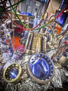
While I don’t understand (again) the image the researchers have included as an illustration of their work, I do find the ‘blue jewels in a pile of junk’ very appealing,

Beamline 10.0.1 at Berkeley Lab’s Advanced Light Source is optimized for the study of for electron structures and correlated electron systems. (Photo by Roy Kaltschmidt) Courtesy: Berkeley Lab

Beamline 10.0.1 at Berkeley Lab’s Advanced Light Source is optimized for the study of for electron structures and correlated electron systems. (Photo by Roy Kaltschmidt) Courtesy: Berkeley Lab

Here’s a link to and a citation for the paper,

Discovery of a Three-dimensional Topological Dirac Semimetal, Na3Bi by Zhongkai Liu, Bo Zhou, Yi Zhang, Zhijun Wang, Hongming Weng, Dharmalingam Prabhakaran, Sung-Kwan Mo, Zhi-Xun Shen, Zhong Fang, Xi Dai, and Zahid Hussain. Published Online January 16 2014 Science DOI: 10.1126/science.1245085

This paper is behind a paywall.

Fly me to the moon using 17th century science

Apparently the first serious scientific thinking about space exploration (in Europe?) was written almost four hundred years ago by John Wilkins, a priest in the Church of England. This year, 2014, marks the four hundredth anniversary of Wilkins birth on January 1 and provides the occasion for a paper, Fly me to the moon? by Allan Chapman, historian and professor at Oxford University (UK).

From a Jan. 14, 2014 news item on ScienceDaily about this Jacobean space exploration programme,

The seventeenth century saw unprecedented changes in our understanding of the universe, spurred on by the invention of the telescope and the opportunity to study stars and planets in detail for the first time. Figures like Galileo are famous for their work not just in astronomy but in scientific experiments of many kinds that challenged established ideas and helped lead to the final demise of an Earth-centred view of the cosmos.

Now historian Prof. Allan Chapman of Wadham College, University of Oxford, has investigated a less well-known pioneer, John Wilkins, who was born 400 years ago this month. His achievements include a plan for ‘mechanical’ space travel, the popularisation of astronomy, managing to negotiate the politics and privations of the English Civil War and helping to found the Royal Society. Prof. Chapman will describe Wilkins’ life in a presentation at the Royal Astronomical Society on Friday 10 January [2014].

The January ?, 2014 Royal Astronomical Society press release, which originated the news item, adds some details about Wilkins,

John Wilkins was born in Canons Ashby, Northamptonshire, on 1 January 1614. A graduate of Magdalen Hall, Oxford, he was ordained as a priest in the Church of England, before travelling widely in the UK and to Germany to meet contemporary scholars. In 1638 he published ‘The Discovery of a New World’ and then in 1640 ‘A Discourse Concerning a New Planet’. The frontispiece of the later book shows his affinity for the Copernican model of the Solar system, with the Polish astronomer and Galileo both prominent. Just as significantly, the illustration shows the stars extending to infinity, rather than being in a then conventional ‘fixed sphere’ just beyond Saturn.

With the two works, Wilkins used clear, concise English to popularise a new understanding of the universe, arguing passionately against the theories of Aristotle that dated back 2000 years. He understood how these ancient ideas (for example that it was in the nature of heavy objects to fall, whereas light materials like smoke would rise) had been fundamentally undermined by scientific discoveries. The model of the cosmos had completely changed over the course of the century since Copernicus.

He [Chapman] sees John Wilkins as one of the first people to understand the power of mass communication for astronomy and as an intellectual ancestor of the late Sir Patrick Moore and Carl Sagan. “Wilkins was a pioneer of English language science communication. Anybody who could read the Bible or enjoy a Shakespeare play could relate to Wilkins’ vision of the new astronomy of Copernicus and Galileo.’

Remarkably, Wilkins also speculated on space travel in his 1640 work. He considered the problems of travel to the Moon, including overcoming the gravitational pull of the Earth, the coldness of space and what the ‘sky voyagers’ would eat during a journey that he thought would take about 180 days.

In 1648, after becoming Master of Wadham College in Oxford, Wilkins expanded these ideas in ‘Mathematical Magick’, a book which describes machines and how systems of gears, pulleys and springs make at first sight insurmountable tasks possible. There he discusses a ‘flying chariot’, a ship like vehicle with bird’s wings, powered by springs and gears that would carry the astronauts on their six month journey. Robert Hooke’s posthumous diary suggests that he and Wilkins may even have built a model of this aircraft. [emphasis mine]

Chapman comments, “John Wilkins was the first person to discuss space travel from a scientific and technological perspective rather than as an aspect of fantasy literature. In his writing he initiates a ‘Jacobean Space Programme’, a serious proposal for travelling to other worlds”.

Here’s an image Chapman has created to illustrate what he believes was Wilkins vision for space travel,

http://www.ras.org.uk/news-and-press/news-archive/254-news-2014/2380-the-jacobean-space-programme-the-life-of-john-wilkins [downloaded from http://www.ras.org.uk/news-and-press/news-archive/254-news-2014/2380-the-jacobean-space-programme-the-life-of-john-wilkins]

Wilkins and Robert Hooke fly to the Moon from Wadham College. Wilkins left no picture of his “Flying Chariot”, so Prof. Chapman assembled components from written descriptions into this drawing. Credit: A. Chapman.[downloaded from http://www.ras.org.uk/news-and-press/news-archive/254-news-2014/2380-the-jacobean-space-programme-the-life-of-john-wilkins]

As one might expect from an historian, Chapman contextualizes Wilkins’ accomplishments within the major political events of the day,

1642 saw the onset of the English Civil War, a conflict that led to the abolition of the Anglican Church, the beheading of King Charles I and the Archbishop of Canterbury and the ascendancy of Oliver Cromwell as Lord Protector. A consummate diplomat, Wilkins even managed to marry Cromwell’s sister, took on the post at Wadham after opponents of Cromwell were purged and yet made the College a centre of tolerance that hosted a club of scientists.

After the restoration of the monarchy in 1659, Wilkins was removed from his next post as Master of Trinity College, Cambridge but nonetheless went on to found and become Secretary of the Royal Society and was appointed Bishop of Chester in 1668. He died in 1671.

While it’s too late to attend Chapman’s Jan. 10, 2014 talk and there doesn’t seem to be an online video of the talk, there’s Chapman’s 6 pp. paper, Fly me to the moon? for anyone who want’s to know more.

New way to practice brain surgery skills before working on live patients

It’s a little disconcerting to learn that neurosurgeons don’t have many options to test drive their skills before they start practicing on patients as a Dec. 10, 2013 news release on EurekAlert about 3D printing (and a new way for neurosurgeons to practice) notes,,

Researchers from the University of Malaya in Malaysia, with collaboration from researchers from the University of Portsmouth and the University of Oxford in the United Kingdom, announce the creation of a cost-effective two-part model of the skull for use in practicing neurosurgical techniques. The model, produced using the latest generation of multimaterial 3D printers, is composed of a variety of materials that simulate the various consistencies and densities of human tissues encountered during neurosurgery. Details on the model are provided in “Utility of multimaterial 3D printers in creating models with pathological entities to enhance the training experience of neurosurgeons. Technical note.” By Vicknes Waran, F.R.C.S.(Neurosurgery), Vairavan Narayanan, F.R.C.S.(Neurosurgery), M.Surg., Ravindran Karuppiah, M.Surg., Sarah L. F. Owen, D.Phil., and Tipu Aziz, F.Med.Sci., published today [Dec. 10, 2013] online, ahead of print, in the Journal of Neurosurgery.

Here’s the disconcerting part (from the news release),

Neurosurgery is a difficult discipline to master. Trainees may spend as many as 10 years after graduation from medical school developing and honing their surgical skills before they can be designated as proficient in their specialty. The greater the number and variety of neurosurgical training sessions, the better the training experience. However, the authors point out that it is difficult to find suitable simulation models that offer accuracy and realism for neurosurgical training while keeping training costs down.

The news release provides a description of what makes the current generation of 3D printers particularly attractive for creating practice skulls, etc.,

Three-dimensional printers have been used to create models of normal and pathological human tissues and organs for physician training and patient instruction for some time. Until recently, however, only one material could be used in the creation of models. While useful for display purposes, one-material models have little value for hands-on training. With the advent of multimaterial 3D printers, the sophistication and versatility of the new models that could be created increased substantially, but so did their price.

Waran and colleagues tell us that this situation is now changing. They state that the newest generation of multimaterial 3D printers can aid neurosurgical training by creating models that simulate different diseases in a variety of body tissues, and they can do this in a cost-effective manner.

With the aid of an Objet500 Connex™ multimaterial 3D printer (Stratasys, Ltd.), researchers at the University of Malaya created a two-part model that can simulate pathological conditions in actual patients. The base piece of the model (the “head”) consists of one material. It has human features (a “face”) and the natural contours of a human skull. This piece is used to train the novice in neuronavigation techniques and can be reused again and again. The second part of the model defines the region in which simulated surgery is performed. This piece contains several different materials, which separately simulate skin, bone, dura mater, tumor, and normal brain tissue. The second piece fits into a slot in the base piece; this multi-textured piece can only be used once and is discarded after the practice session. Fortunately, it is easy to reproduce a steady stream of new pieces.

To make the training session valuable, the trainee must be able to see, feel, and even hear different “tissue” responses to surgical instruments and techniques during simulation surgery. The researchers tell us that the “skin” is designed to be pliable enough to be cut by a scalpel and repaired by sutures, yet sturdy enough to be held by a retractor; the “bone” has to be hard enough for the trainee to obtain experience using bone perforators and cutters; the “dura mater” must be thin and pliable—just like the real thing. The consistency and color of the “tumor” differ from those of the “brain” to simulate actual tissues. The researchers made the “tumor” softer than the “brain” and colored it orange, whereas they colored the brain light yellow.

To test the quality of the model produced by the printer and to make minor adjustments, the researchers from Malaysia were aided by other researchers from the UK. Three neurosurgeons and one expert in surgical simulations performed simulated surgery and assessed the model’s “tissue” components. All parts received ratings of “fair” or “good,” with most rated “good.”

The usefulness of the model in training neuronavigation techniques was also assessed. Since the two-part model was based on data from a real patient, it was no surprise that “neuroimaging” was rated “excellent” by the evaluating team. Two navigation systems were used, and in both cases “registration was accurate and planning possible.”

Waran and colleagues state that the reusable base piece of the model costs approximately US $2000 to fabricate and the disposable inset costs US $600. This makes these training models affordable. In addition, model designs are based on actual patient data, providing limitless variety.

Here’s a link to and a citation for the paper,

Waran V, Narayana V, Karuppiah R, Owen SLF, Aziz T: Utility of multimaterial 3D printers in creating models with pathological entities to enhance the training experience of neurosurgeons. Technical note. Journal of Neurosurgery, published online, ahead of print, December 10, 2013; DOI: 10.3171/2013.11.JNS131066.

This appears to be an open access paper.

Surviving 39 minutes at room temperature—recordbreaking for quantum materials

There are two news releases about this work which brings quantum computing a step closer to reality. I’ll start with the Nov. 15, 2013 Simon Fraser University (SFU; located in Vancouver, Canada) news release (Note: A link has been removed),,

An international team of physicists led by Simon Fraser University professor Mike Thewalt has overcome a key barrier to building practical quantum computers, taking a significant step to bringing them into the mainstream.

In their record-breaking experiment conducted on SFU’s Burnaby campus, [part of Metro Vancouver] the scientists were able to get fragile quantum states to survive in a solid material at room temperature for 39 minutes. For the average person, it may not seem like a long time, but it’s a veritable eternity to a quantum physicist.

“This opens up the possibility of truly long-term coherent information storage at room temperature,” explains Thewalt.

Quantum computers promise to significantly outperform today’s machines at certain tasks, by exploiting the strange properties of subatomic particles. Conventional computers process data stored as strings of ones or zeroes, but quantum objects are not constrained to the either/or nature of binary bits.

Instead, each quantum bit – or qubit – can be put into a superposition of both one and zero at the same time, enabling them to perform multiple calculations simultaneously. For instance, this ability to multi-task could allow quantum computers to crack seemingly secure encryption codes.

“A powerful universal quantum computer would change technology in ways that we already understand, and doubtless in ways we do not yet envisage,” says Thewalt, whose research was published in Science today.

“It would have a huge impact on security, code breaking and the transmission and storage of secure information. It would be able to solve problems which are impossible to solve on any conceivable normal computer. It would be able to model the behaviour of quantum systems, a task beyond the reach of normal computers, leading, for example, to the development of new drugs by a deeper understanding of molecular interactions.”

However, the problem with attempts to build these extraordinary number-crunchers is that superposition states are delicate structures that can collapse like a soufflé if nudged by a stray particle, such as an air molecule.

To minimize this unwanted process, physicists often cool their qubit systems to almost absolute zero (-273 C) and manipulate them in a vacuum. But such setups are finicky to maintain and, ultimately, it would be advantageous for quantum computers to operate robustly at everyday temperatures and pressures.

“Our research extends the demonstrated coherence time in a solid at room temperature by a factor of 100 – and at liquid helium temperature by a factor of 60 (from three minutes to three hours),” says Thewalt.

“These are large, significant improvements in what is possible.”

The November 15, 2013 University of Oxford news release (also on EurekAlert), features their own researcher and more information (e.g., the previous record for maintaining coherence of a solid state at room temperature),

An international team including Stephanie Simmons of Oxford University report in this week’s Science a test performed as part of a project led by Mike Thewalt of Simon Fraser University, Canada, and colleagues. …

In the experiment, the team raised the temperature of a system, in which information is encoded in the nuclei of phosphorus atoms in silicon, from -269°C to 25°C and demonstrated that the superposition states survived at this balmy temperature for 39 minutes – outside of silicon the previous record for such a state’s survival at room temperature was around two seconds. [emphasis mine] The team even found that they could manipulate the qubits as the temperature of the system rose, and that they were robust enough for this information to survive being ‘refrozen’ (the optical technique used to read the qubits only works at very low temperatures).

‘Thirty-nine minutes may not seem very long but as it only takes one-hundred-thousandth of a second to flip the nuclear spin of a phosphorus ion – the type of operation used to run quantum calculations – in theory over two million operations could be applied in the time it takes for the superposition to naturally decay by 1%. Having such robust, as well as long-lived, qubits could prove very helpful for anyone trying to build a quantum computer,’ said Stephanie Simmons of Oxford University’s Department of Materials, an author of the paper.

The team began with a sliver of silicon doped with small amounts of other elements, including phosphorus. Quantum information was encoded in the nuclei of the phosphorus atoms: each nucleus has an intrinsic quantum property called ‘spin’, which acts like a tiny bar magnet when placed in a magnetic field. Spins can be manipulated to point up (0), down (1), or any angle in between, representing a superposition of the two other states.

The team prepared their sample at just 4°C above absolute zero (-269°C) and placed it in a magnetic field. Additional magnetic field pulses were used to tilt the direction of the nuclear spin and create the superposition states. When the sample was held at this cryogenic temperature, the nuclear spins of about 37% of the ions – a typical benchmark to measure quantum coherence – remained in their superposition state for three hours. The same fraction survived for 39 minutes when the temperature of the system was raised to 25°C.

There is still some work ahead before the team can carry out large-scale quantum computations. The nuclear spins of the 10 billion or so phosphorus ions used in this experiment were all placed in the same quantum state. To run calculations, however, physicists will need to place different qubits in different states. ‘To have them controllably talking to one another – that would address the last big remaining challenge,’ said Simmons.

Even for the uninitiated, going from a record of two seconds to 39 minutes has to raise an eyebrow.

Here’s a link to and a citation for the paper,

Room-Temperature Quantum Bit Storage Exceeding 39 Minutes Using Ionized Donors in Silicon-28.by Kamyar Saeedi, Stephanie Simmons, Jeff Z. Salvail, Phillip Dluhy, Helge Riemann, Nikolai V. Abrosimov, Peter Becker, Hans-Joachim Pohl, John J. L. Morton, & Mike L. W. Thewalt.  Science 15 November 2013: Vol. 342 no. 6160 pp. 830-833 DOI: 10.1126/science.1239584

This paper is behind a paywall.

ETA Nov. 18 ,2013:  The University College of London has also issued a Nov. 15, 2013 news release on EurekAlert about this work. While some of this is repetitive, I think there’s enough new information to make this excerpt worthwhile,

The team even found that they could manipulate the qubits as the temperature of the system rose, and that they were robust enough for this information to survive being ‘refrozen’ (the optical technique used to read the qubits only works at very low temperatures). 39 minutes may not sound particularly long, but since it only takes a tiny fraction of a second to run quantum computations by flipping the spin of phosphorus ions (electrically charged phosphorus atoms), many millions of operations could be carried out before a system like this decays.

“This opens up the possibility of truly long-term coherent information storage at room temperature,” said Mike Thewalt (Simon Fraser University), the lead researcher in this study.

The team began with a sliver of silicon doped with small amounts of other elements, including phosphorus. They then encoded quantum information in the nuclei of the phosphorus atoms: each nucleus has an intrinsic quantum property called ‘spin’, which acts like a tiny bar magnet when placed in a magnetic field. Spins can be manipulated to point up (0), down (1), or any angle in between, representing a superposition of the two other states.

The team prepared their sample at -269 °C, just 4 degrees above absolute zero, and placed it in a magnetic field. They used additional magnetic field pulses to tilt the direction of the nuclear spin and create the superposition states. When the sample was held at this cryogenic temperature, the nuclear spins of about 37 per cent of the ions – a typical benchmark to measure quantum coherence – remained in their superposition state for three hours. The same fraction survived for 39 minutes when the temperature of the system was raised to 25 °C.


Nano-solutions for the 21st century, University of Oxford Martin School, and Eric Drexler

Eric Drexler (aka, K. Eric Drexler) is a big name in the world of nanotechnology as per my May 6, 2013 posting abut his talk in Seattle as part of a tour promoting his latest book,

Here’s more from the University Bookstore’s event page,

Eric Drexler is the founding father of nanotechnology, the science of engineering on a molecular level—and the science thats about to change the world. Already, says Drexler, author of Radical Abundance, scientists have constructed prototypes for circuit boards built of millions of precisely arranged atoms. This kind of atomic precision promises to change the way we make things (cleanly, inexpensively, and on a global scale), the way we buy things (solar arrays could cost no more than cardboard and aluminum foil, with laptops about the same)—and the very foundations of our economy and environment.

… Drexler’s latest effort, Radical Abundance, here’s what he had to say about the book in a July 21, 2011 posting on his Meta Modern blog,

Radical Abundance will integrate and extend several themes that I’ve touched on in Metamodern, but will go much further. The topics include:

  • The nature of science and engineering, and the prospects for a deep transformation in the material basis of civilization.
  • Why all of this is surprisingly understandable.
  • A personal narrative of the emergence of the molecular nanotechnology concept and the turbulent history of progress and politics that followed
  • The quiet rise of macromolecular nanotechnologies, their power, and the rapidly advancing state of the art
  • ….

About the same time he was promoting his book, Radical Abundance, the University of Oxford Martin School released a report written by Drexler and co-authored with Dennis Pamplin,, which is featured in an Oct. 28, 2013 news item on Nanowerk (Note: A link has been removed),

The world faces unprecedented global challenges related to depleting natural resources, pollution, climate change, clean water, and poverty. These problems are directly linked to the physical characteristics of our current technology base for producing energy and material products. Deep and pervasive changes in this technology base can address these global problems at their most fundamental, physical level, by changing both the products and the means of production used by 21st century civilization. The key development is advanced, atomically precise manufacturing (APM).

This report (“Nano-solutions for the 21st century”; pdf) examines the potential for nanotechnology to enable deeply transformative production technologies that can be developed through a series of advances that build on current nanotechnology research.

Coincidentally or not, Eric Drexler is writing a series of posts for the Guardian about nanotechnology and the future. Here’s a sampling from his Oct. 28, 2013 post on the Guardian’s Small World Nanotech blog sponsored by NanOpinion,

In my initial post in this series, I asked, “What if nanotechnology could deliver on its original promise, not only new, useful, nanoscale products, but a new, transformative production technology able to displace industrial production technologies and bring radical improvements in production cost, scope, and resource efficiency?”

The potential implications are immense, not just for computer chips and other nanotechnologies, but for issues on the scale of global development and climate change. My first post outlined the nature of this technology, atomically precise manufacturing (APM), comparing it with today’s 3D printing and digital nanoelectronics.

My second post placed APM-level technologies in the context of today’s million-atom atomically precise fabrication technologies and outlined the direction of research, an open path, but by no means short, that leads to larger atomically precise structures, a growing range of product materials and a wider range of functional devices, culminating in the factory-in-a-box technologies of APM.

Together, these provided an introduction to the modern view of APM-level technologies. Here, I’d like to say a few words about the implications of APM-level technologies for human life and global society.

At the bottom of the posting, this is noted,

Eric Drexler, often called “the father of nanotechnology”, is at the Oxford Martin Programme on the Impacts of Future Technology, University of Oxford. His most recent book is Radical Abundance: How a Revolution in Nanotechnology Will Change Civilization

The Oxford Martin School of Oxford University and the Research Center for Sustainable Development of the China Academy of Social Sciences recently released a report on atomically precise manufacturing, Nano-solutions for the 21st century. The report discusses the status and prospects for atomically precise manufacturing (APM) together with some of its implications for economic and international affairs.

Publicity is a beautiful thing, especially when you can tie so many things together. Drexler, his book, the report, and the Guardian’s special section sponsored by NanOpinion.

Getting back to the report, Nano-solutions for the 21st century, I notice that there’s been a lot of collaboration with Chinese researchers and institutions if the acknowledgements are a way to judge these things,

This work results from an extensive process that has included interaction and contributions by scientists,
governments, philanthropists, and forward-thinkers around the world. Over the last three years workshops
have been conducted in China, India, US, Europe, Japan, and more to discuss these findings and their
global implications. Draft findings have also been presented at many meetings, from UNFCCC events to
specialist conferences. The wealth of feedback received from this project has been of utmost importance
and we see the resulting report as a collaboration project than as the work of two individuals.

The authors wish to thank all those who have participated in the process and extend particular thanks
to China and India, especially Institute for Urban & Environmental Studies, Chinese Academy of Social
Sciences (CASS) and the team from the National Center for Nanoscience and Technology (NCNST)
including Dr. ZHI Linjie, Dr. TANG Zhiyong, Dr. WEI Zhixiang and Dr. HAN Baohang. Professor Linjie Zhi
was also kind enough to translate the abstract. In India the Rajiv Gandhi Foundation and CII – ITC Centre
of Excellence for Sustainable Development where among those providing valuable input.

This report is only a start of what we hope is a vital international discussion about one of the most
interesting fields of the 21st century. We would therefor like to extend special thanks to the Chinese
Academy of Social Sciences (CASS), Chinese Academy of Sciences (CAS) and The Oxford Martin School
that are examples of world leading institutions that support further discussions in this important area.

Dr. Eric Drexler and Dennis Pamlin worked together to make this report a reality. Drexler, currently at the
Oxford Martin School, provided technical leadership and served as primary author of the report. Pamlin
contributed through discussions, structure and input regarding overall trends in relation to the key aspects
of report. Both authors want to thank Dr. Stephanie Corchnoy who contributed to the research and final
editing. As always the sole responsibility for the content of report lies with the authors.

Eric Drexler
Dennis Pamlin (p. 1)

I find the specific call outs to China, India, and Japan quite interesting since any European partners are covered under the term for the entire continent, Europe. I haven’t read the report but for what it’s worth here’s the abstract,

The report has five sections:
1. Nanotechnology and global challenge
The first section discusses the basics of advanced, atomically precise nanotechnology and
explains how current and future solutions can help address global challenges. Key concepts
are presented and different kinds of nanotechnology are discussed and compared.
2. The birth of Nanotechnology
The second section discusses the development of nanotechnology, from the first vision
fifty years ago, expanding via a scientific approach to atomically precise manufacturing
thirty years ago, initial demonstrations of principle twenty years ago, to the last decade
of of accelerating success in developing key enabling technologies. The important role
of emerging countries is discussed, with China as a leading example, together with an
overview of the contrast between the promise and the results to date.
3. Delivery of transformative nanotechnologies
Here the different aspects of APM that are needed to enable breakthrough advances in
productive technologies are discussed. The necessary technology base can be developed
through a series of coordinated advances along strategically chosen lines of research.
4. Accelerating progress toward advanced nanotechnologies
This section discusses research initiatives that can enable and support advanced
nanotechnology, on paths leading to APM, including integrated cross-disciplinary research
and Identification of high-value applications and their requirements.
5. Possible next steps
The final section provides a short summary of the opportunities and the possibilities to
address institutional challenges of planning, resource allocation, evaluation, transparency,
and collaboration as nanotechnology moves into its next phase of development: nanosystems engineering.

The report in its entirety provides a comprehensive overview of the current global condition, as well as
notable opportunities and challenges. This content is divided into five independent sections that can
be read and understood individually, allowing those with specific interests to access desired information
more directly and easily. With all five sections taken together, the report as a whole describes low-
cost actions that can help solve critical problems, create opportunities, reduce security risks, and help
countries join and accelerate cooperative development of this global technological revolution. Of
particular importance, several considerations are highlighted that strongly favor a policy of transparent,
international, collaborative development.

One final comment, I’m not familiar with Drexler’s co-author, Dennis Pamlin so went searching for some details. Here’s a self-description from the About page on his eponymous website,

Dennis Pamlin is an entrepreneur and founder of 21st Century Frontiers. He works with companies, governments and NGOs as a strategic economic, technology and innovation advisor. His background is in engineering, industrial economy and marketing. Mr Pamlin worked as Global Policy Advisor for WWF from 1999 to 2009. During his tenure, Pamlin initiated WWFs Trade and Investment Programme work in the BRICs (Brazil, Russia, India, China and South Africa) and led the work with companies (especially high-tech companies such as ICT) as solution providers.

Pamlin is currently an independent consultant as well as Director for the Low Carbon Leaders Project under the UN Global Compact and is a Senior Associate at Chinese Academy of Social Sciences. Current work includes work to establish a web platform to promote transformative mobile applications, creating the first Low Carbon City Development Index (LCCDI) make transformative low-carbon ICT part of the global climate discussions, leading the Global ICT companies work (through GeSI) to establish the ICT sector as a global solution provider when it comes to resource efficient solutions, advising the EU on how public procurement can increase innovation and the uptake of transformative solutions.

Pamlin is also exploring how new ideas can be financed through web-tools/apps and the cultural tensions between the “west” and the re-emerging economies (with focus on China and India).

He is also leading work to develop methodologies for companies and cities to measure and report their positive impacts, focus on climate, water and poverty, but other areas are also under development.

I also found this on Pamlin’s LinkedIn profile,

Entrepreneur, advisor and transformative explorer

Other
International Affairs

Current

21st century Frontiers,
Chinese Academy of Social Sciences (CASS),
Global Challenges Foundation

Previous

WWF,
Greenpeace

It seems to me there’s a ‘sustainability and nanotechnology theme being implied in the introduction to the report (“The world faces unprecedented global challenges related to depleting natural resources, pollution, climate change, clean water, and poverty.”)  and I’m certainly inferring it from my reading of Pamlin’s background and interests and this phrase in the acknowledgements: “… Rajiv Gandhi Foundation and CII – ITC Centre of Excellence for Sustainable Development where among those providing valuable input … .”

Oddly, I last mentioned nanotechnology and sustainability In an Oct. 28, 2013 posting about a nanotechnology-enabled consumer products database where I also made note of the Second Sustainable Nanotechnology Organization Conference whose website can be found here.
Only for the truly obsessed: a movie featuring gold nanocrystal vibrations

Folks at the London Centre for Nanotechnology (at the University College of London) have released a film made with a pioneering 3D imaging technique that shows how gold nanocrystals vibrate. From the May 23, 2013 news release on EurekAlert,

A billon-frames-per-second film has captured the vibrations of gold nanocrystals in stunning detail for the first time.

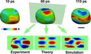
The film, which was made using 3D imaging pioneered at the London Centre for Nanotechnology (LCN) at UCL [University College of London], reveals important information about the composition of gold. The findings are published in the journal Science.

Jesse Clark, from the LCN and lead author of the paper said: “Just as the sound quality of a musical instrument can provide great detail about its construction, so too can the vibrations seen in materials provide important information about their composition and functions.”

“It is absolutely amazing that we are able to capture snapshots of these nanoscale motions and create movies of these processes. This information is crucial to understanding the response of materials after perturbation. “

Caption: The acoustic phonons can be visualized on the surface as regions of contraction (blue) and expansion (red). Also shown are two-dimensional images comparing the experimental results with theory and molecular dynamics simulation. The scale bar is 100 nanometers. Credit: Jesse Clark/UCL

Caption: The acoustic phonons can be visualized on the surface as regions of contraction (blue) and expansion (red). Also shown are two-dimensional images comparing the experimental results with theory and molecular dynamics simulation. The scale bar is 100 nanometers. Credit: Jesse Clark/UCL

Here are more details from the news release,

Scientists found that the vibrations were unusual because they start off at exactly the same moment everywhere inside the crystal. It was previously expected that the effects of the excitation would travel across the gold nanocrystal at the speed of sound, but they were found to be much faster, i.e., supersonic.

The new images support theoretical models for light interaction with metals, where energy is first transferred to electrons, which are able to short-circuit the much slower motion of the atoms.

The team carried out the experiments at the SLAC National Accelerator Laboratory using a revolutionary X-ray laser called the “Linac Coherent Light Source”. The pulses of X-rays are extremely short (measured in femtoseconds, or quadrillionths of a second), meaning they are able to freeze all motion of the atoms in any sample, leaving only the electrons still moving.

However, the X-ray pulses are intense enough that the team was able to take single snapshots of the vibrations of the gold nanocrystals they were examining. The vibration was started with a short pulse of infrared light.

The real keeners can watch the movie if they click on the link to the May 23, 2013 news release on EurekAlert.

The team developing this movie was international in scope (from the news release),

The research team included contributors from UCL, University of Oxford, SLAC, Argonne National Laboratory [US] and LaTrobe University, Australia.

Are we and our world a computer simulation?

There is a fascinating Dec. 10, 2012 news item on Nanowerk about a philosophical question that’s being researched by a team of physicists at the University of Washington (Note: I have removed a link),

The concept that current humanity could possibly be living in a computer simulation comes from a 2003 paper published in Philosophical Quarterly (“Are You Living In a Computer Simulation?“) by Nick Bostrom, a philosophy professor at the University of Oxford. In the paper, he argued that at least one of three possibilities is true:

The human species is likely to go extinct before reaching a “posthuman” stage.

Any posthuman civilization is very unlikely to run a significant number of simulations of its evolutionary history.

We are almost certainly living in a computer simulation.

He also held that “the belief that there is a significant chance that we will one day become posthumans who run ancestor simulations is false, unless we are currently living in a simulation.”

Here’s what the University of Washington physicists, from the Dec. 10, 2012 University of Washington news release by Vincent Stricherz, which originated the news item,

With current limitations and trends in computing, it will be decades before researchers will be able to run even primitive simulations of the universe. But the UW team has suggested tests that can be performed now, or in the near future, that are sensitive to constraints imposed on future simulations by limited resources.

Currently, supercomputers using a technique called lattice quantum chromodynamics and starting from the fundamental physical laws that govern the universe can simulate only a very small portion of the universe, on the scale of one 100-trillionth of a meter, a little larger than the nucleus of an atom, said Martin Savage, a UW physics professor.

However, Savage said, there are signatures of resource constraints in present-day simulations that are likely to exist as well in simulations in the distant future, including the imprint of an underlying lattice if one is used to model the space-time continuum.

The supercomputers performing lattice quantum chromodynamics calculations essentially divide space-time into a four-dimensional grid. That allows researchers to examine what is called the strong force, one of the four fundamental forces of nature and the one that binds subatomic particles called quarks and gluons together into neutrons and protons at the core of atoms.

“If you make the simulations big enough, something like our universe should emerge,” Savage said. Then it would be a matter of looking for a “signature” in our universe that has an analog in the current small-scale simulations.

Savage and colleagues Silas Beane of the University of New Hampshire, who collaborated while at the UW’s Institute for Nuclear Theory, and Zohreh Davoudi, a UW physics graduate student, suggest that the signature could show up as a limitation in the energy of cosmic rays.

In a paper they have posted on arXiv, an online archive for preprints of scientific papers in a number of fields, including physics, they say that the highest-energy cosmic rays would not travel along the edges of the lattice in the model but would travel diagonally, and they would not interact equally in all directions as they otherwise would be expected to do.

“This is the first testable signature of such an idea,” Savage said.

If such a concept turned out to be reality, it would raise other possibilities as well. For example, Davoudi suggests that if our universe is a simulation, then those running it could be running other simulations as well, essentially creating other universes parallel to our own.

“Then the question is, ‘Can you communicate with those other universes if they are running on the same platform?’” she said. [emphasis mine]

Here’s the citation for and a link to the arXiv.org paper by Beane, Davoudi, and Savage,

Constraints on the Universe as a Numerical Simulation by Silas R. Beane, Zohreh Davoudi, Martin J. Savage (Submitted on 4 Oct 2012 (v1), last revised 9 Nov 2012 (this version, v2))

Fascinating, yes?