Tag Archives: molybdenum disulfide

Memristors with better mimicry of synapses

It seems to me it’s been quite a while since I’ve stumbled across a memristor story from the University of Micihigan but it was worth waiting for. (Much of the research around memristors has to do with their potential application in neuromorphic (brainlike) computers.) From a December 17, 2018 news item on ScienceDaily,

A new electronic device developed at the University of Michigan can directly model the behaviors of a synapse, which is a connection between two neurons.

For the first time, the way that neurons share or compete for resources can be explored in hardware without the need for complicated circuits.

“Neuroscientists have argued that competition and cooperation behaviors among synapses are very important. Our new memristive devices allow us to implement a faithful model of these behaviors in a solid-state system,” said Wei Lu, U-M professor of electrical and computer engineering and senior author of the study in Nature Materials.

A December 17, 2018 University of Michigan news release (also on EurekAlert), which originated the news item, provides an explanation of memristors and their ‘similarity’ to synapses while providing more details about this latest research,

Memristors are electrical resistors with memory–advanced electronic devices that regulate current based on the history of the voltages applied to them. They can store and process data simultaneously, which makes them a lot more efficient than traditional systems. They could enable new platforms that process a vast number of signals in parallel and are capable of advanced machine learning.

The memristor is a good model for a synapse. It mimics the way that the connections between neurons strengthen or weaken when signals pass through them. But the changes in conductance typically come from changes in the shape of the channels of conductive material within the memristor. These channels–and the memristor’s ability to conduct electricity–could not be precisely controlled in previous devices.

Now, the U-M team has made a memristor in which they have better command of the conducting pathways.They developed a new material out of the semiconductor molybdenum disulfide–a “two-dimensional” material that can be peeled into layers just a few atoms thick. Lu’s team injected lithium ions into the gaps between molybdenum disulfide layers.
They found that if there are enough lithium ions present, the molybdenum sulfide transforms its lattice structure, enabling electrons to run through the film easily as if it were a metal. But in areas with too few lithium ions, the molybdenum sulfide restores its original lattice structure and becomes a semiconductor, and electrical signals have a hard time getting through.

The lithium ions are easy to rearrange within the layer by sliding them with an electric field. This changes the size of the regions that conduct electricity little by little and thereby controls the device’s conductance.

“Because we change the ‘bulk’ properties of the film, the conductance change is much more gradual and much more controllable,” Lu said.

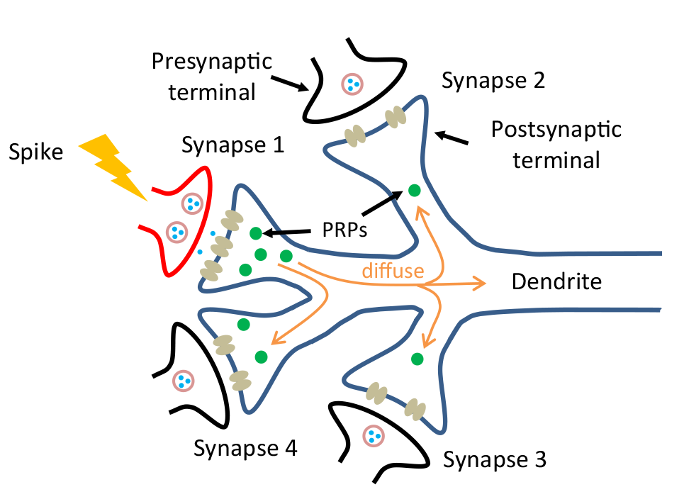
In addition to making the devices behave better, the layered structure enabled Lu’s team to link multiple memristors together through shared lithium ions–creating a kind of connection that is also found in brains. A single neuron’s dendrite, or its signal-receiving end, may have several synapses connecting it to the signaling arms of other neurons. Lu compares the availability of lithium ions to that of a protein that enables synapses to grow.

If the growth of one synapse releases these proteins, called plasticity-related proteins, other synapses nearby can also grow–this is cooperation. Neuroscientists have argued that cooperation between synapses helps to rapidly form vivid memories that last for decades and create associative memories, like a scent that reminds you of your grandmother’s house, for example. If the protein is scarce, one synapse will grow at the expense of the other–and this competition pares down our brains’ connections and keeps them from exploding with signals.
Lu’s team was able to show these phenomena directly using their memristor devices. In the competition scenario, lithium ions were drained away from one side of the device. The side with the lithium ions increased its conductance, emulating the growth, and the conductance of the device with little lithium was stunted.

In a cooperation scenario, they made a memristor network with four devices that can exchange lithium ions, and then siphoned some lithium ions from one device out to the others. In this case, not only could the lithium donor increase its conductance–the other three devices could too, although their signals weren’t as strong.

Lu’s team is currently building networks of memristors like these to explore their potential for neuromorphic computing, which mimics the circuitry of the brain.

Here’s a link to and a citation for the paper,

Ionic modulation and ionic coupling effects in MoS2 devices for neuromorphic computing by Xiaojian Zhu, Da Li, Xiaogan Liang, & Wei D. Lu. Nature Materials (2018) DOI: https://doi.org/10.1038/s41563-018-0248-5 Published 17 December 2018

This paper is behind a paywall.

The researchers have made images illustrating their work available,

A schematic of the molybdenum disulfide layers with lithium ions between them. On the right, the simplified inset shows how the molybdenum disulfide changes its atom arrangements in the presence and absence of the lithium atoms, between a metal (1T’ phase) and semiconductor (2H phase), respectively. Image credit: Xiaojian Zhu, Nanoelectronics Group, University of Michigan.

A diagram of a synapse receiving a signal from one of the connecting neurons. This signal activates the generation of plasticity-related proteins (PRPs), which help a synapse to grow. They can migrate to other synapses, which enables multiple synapses to grow at once. The new device is the first to mimic this process directly, without the need for software or complicated circuits. Image credit: Xiaojian Zhu, Nanoelectronics Group, University of Michigan.
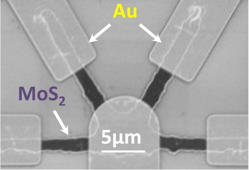
An electron microscope image showing the rectangular gold (Au) electrodes representing signalling neurons and the rounded electrode representing the receiving neuron. The material of molybdenum disulfide layered with lithium connects the electrodes, enabling the simulation of cooperative growth among synapses. Image credit: Xiaojian Zhu, Nanoelectronics Group, University of Michigan.

That’s all folks.

‘Seamless’ bioeletronics made possible with protein bridge

For some years now I’ve been tagging certain posts with ‘machine/flesh’ as more bioelectronic devices are being invented for use as implants of various kinds.

Researchers at the University of Washington (state) have found a means of making bioelectronics implants a more comfortable fit in the body according to an Oct. 4, 2016 news item on phys.org,

Life has always played by its own set of molecular rules. From the biochemistry behind the first cells, evolution has constructed wonders like hard bone, rough bark and plant enzymes that harvest light to make food.

But our tools for manipulating life—to treat disease, repair damaged tissue and replace lost limbs—come from the nonliving realm: metals, plastics and the like. Though these save and preserve lives, our synthetic treatments are rooted in a chemical language ill-suited to our organic elegance. Implanted electrodes scar, wires overheat and our bodies struggle against ill-fitting pumps, pipes or valves.

A solution lies in bridging this gap where artificial meets biological—harnessing biological rules to exchange information between the biochemistry of our bodies and the chemistry of our devices. In a paper published Sept. 22 [2016] in Scientific Reports, engineers at the University of Washington unveiled peptides—small proteins which carry out countless essential tasks in our cells—that can provide just such a link.

An Oct. 3, 2016 University of Washington (state) news release (also on EurekAlert), which originated the news item, expands on the theme,

The team, led by UW professor Mehmet Sarikaya in the Departments of Materials Science & Engineering, shows how a genetically engineered peptide can assemble into nanowires atop 2-D, solid surfaces that are just a single layer of atoms thick. These nanowire assemblages are critical because the peptides relay information across the bio/nano interface through molecular recognition — the same principles that underlie biochemical interactions such as an antibody binding to its specific antigen or protein binding to DNA.

Since this communication is two-way, with peptides understanding the “language” of technology and vice versa, their approach essentially enables a coherent bioelectronic interface.

“Bridging this divide would be the key to building the genetically engineered biomolecular solid-state devices of the future,” said Sarikaya, who is also a professor of chemical engineering and oral health sciences.

His team in the UW Genetically Engineered Materials Science and Engineering Center studies how to coopt the chemistry of life to synthesize materials with technologically significant physical, electronic and photonic properties. To Sarikaya, the biochemical “language” of life is a logical emulation.

“Nature must constantly make materials to do many of the same tasks we seek,” he said.

The UW team wants to find genetically engineered peptides with specific chemical and structural properties. They sought out a peptide that could interact with materials such as gold, titanium and even a mineral in bone and teeth. These could all form the basis of future biomedical and electro-optical devices. Their ideal peptide should also change the physical properties of synthetic materials and respond to that change. That way, it would transmit “information” from the synthetic material to other biomolecules — bridging the chemical divide between biology and technology.

In exploring the properties of 80 genetically selected peptides — which are not found in nature but have the same chemical components of all proteins — they discovered that one, GrBP5, showed promising interactions with the semimetal graphene. They then tested GrBP5’s interactions with several 2-D nanomaterials which, Sarikaya said, “could serve as the metals or semiconductors of the future.”

“We needed to know the specific molecular interactions between this peptide and these inorganic solid surfaces,” he added.

Their experiments revealed that GrBP5 spontaneously organized into ordered nanowire patterns on graphene. With a few mutations, GrBP5 also altered the electrical conductivity of a graphene-based device, the first step toward transmitting electrical information from graphene to cells via peptides.

In parallel, Sarikaya’s team modified GrBP5 to produce similar results on a semiconductor material — molybdenum disulfide — by converting a chemical signal to an optical signal. They also computationally predicted how different arrangements of GrBP5 nanowires would affect the electrical conduction or optical signal of each material, showing additional potential within GrBP5’s physical properties.

“In a way, we’re at the flood gates,” said Sarikaya. “Now we need to explore the basic properties of this bridge and how we can modify it to permit the flow of ‘information’ from electronic and photonic devices to biological systems.”

Here’s a link to and a citation for the paper,

Bioelectronic interfaces by spontaneously organized peptides on 2D atomic single layer materials by Yuhei Hayamizu, Christopher R. So, Sefa Dag, Tamon S. Page, David Starkebaum, & Mehmet Sarikaya. Scientific Reports 6, Article number: 33778 (2016) doi:10.1038/srep33778 Published online: 22 September 2016

This paper is open access.

This image illustrates the GrBP5 nanowires,

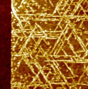
A top view image of GrBP5 nanowires on a 2-D surface of molybdenum disulfide.Mehmet Sarikaya/Scientific Reports

A top view image of GrBP5 nanowires on a 2-D surface of molybdenum disulfide.Mehmet Sarikaya/Scientific Reports

Osmotic power: electricity generated with water, salt and a 3-atoms-thick membrane


EPFL researchers have developed a system that generates electricity from osmosis with unparalleled efficiency. Their work, featured in “Nature”, uses seawater, fresh water, and a new type of membrane just three atoms thick.

A July 13, 2016 news item on Nanowerk highlights  research on osmotic power at École polytechnique fédérale de Lausanne (EPFL; Switzerland),

Proponents of clean energy will soon have a new source to add to their existing array of solar, wind, and hydropower: osmotic power. Or more specifically, energy generated by a natural phenomenon occurring when fresh water comes into contact with seawater through a membrane.

Researchers at EPFL’s Laboratory of Nanoscale Biology have developed an osmotic power generation system that delivers never-before-seen yields. Their innovation lies in a three atoms thick membrane used to separate the two fluids. …

A July 14, 2016 EPFL press release (also on EurekAlert but published July 13, 2016), which originated the news item, describes the research,

The concept is fairly simple. A semipermeable membrane separates two fluids with different salt concentrations. Salt ions travel through the membrane until the salt concentrations in the two fluids reach equilibrium. That phenomenon is precisely osmosis.

If the system is used with seawater and fresh water, salt ions in the seawater pass through the membrane into the fresh water until both fluids have the same salt concentration. And since an ion is simply an atom with an electrical charge, the movement of the salt ions can be harnessed to generate electricity.

A 3 atoms thick, selective membrane that does the job

EPFL’s system consists of two liquid-filled compartments separated by a thin membrane made of molybdenum disulfide. The membrane has a tiny hole, or nanopore, through which seawater ions pass into the fresh water until the two fluids’ salt concentrations are equal. As the ions pass through the nanopore, their electrons are transferred to an electrode – which is what is used to generate an electric current.

Thanks to its properties the membrane allows positively-charged ions to pass through, while pushing away most of the negatively-charged ones. That creates voltage between the two liquids as one builds up a positive charge and the other a negative charge. This voltage is what causes the current generated by the transfer of ions to flow.

“We had to first fabricate and then investigate the optimal size of the nanopore. If it’s too big, negative ions can pass through and the resulting voltage would be too low. If it’s too small, not enough ions can pass through and the current would be too weak,” said Jiandong Feng, lead author of the research.

What sets EPFL’s system apart is its membrane. In these types of systems, the current increases with a thinner membrane. And EPFL’s membrane is just a few atoms thick. The material it is made of – molybdenum disulfide – is ideal for generating an osmotic current. “This is the first time a two-dimensional material has been used for this type of application,” said Aleksandra Radenovic, head of the laboratory of Nanoscale Biology

Powering 50’000 energy-saving light bulbs with 1m2 membrane

The potential of the new system is huge. According to their calculations, a 1m2 membrane with 30% of its surface covered by nanopores should be able to produce 1MW of electricity – or enough to power 50,000 standard energy-saving light bulbs. And since molybdenum disulfide (MoS2) is easily found in nature or can be grown by chemical vapor deposition, the system could feasibly be ramped up for large-scale power generation. The major challenge in scaling-up this process is finding out how to make relatively uniform pores.

Until now, researchers have worked on a membrane with a single nanopore, in order to understand precisely what was going on. ” From an engineering perspective, single nanopore system is ideal to further our fundamental understanding of 8=-based processes and provide useful information for industry-level commercialization”, said Jiandong Feng.

The researchers were able to run a nanotransistor from the current generated by a single nanopore and thus demonstrated a self-powered nanosystem. Low-power single-layer MoS2 transistors were fabricated in collaboration with Andras Kis’ team at at EPFL, while molecular dynamics simulations were performed by collaborators at University of Illinois at Urbana–Champaign

Harnessing the potential of estuaries

EPFL’s research is part of a growing trend. For the past several years, scientists around the world have been developing systems that leverage osmotic power to create electricity. Pilot projects have sprung up in places such as Norway, the Netherlands, Japan, and the United States to generate energy at estuaries, where rivers flow into the sea. For now, the membranes used in most systems are organic and fragile, and deliver low yields. Some systems use the movement of water, rather than ions, to power turbines that in turn produce electricity.

Once the systems become more robust, osmotic power could play a major role in the generation of renewable energy. While solar panels require adequate sunlight and wind turbines adequate wind, osmotic energy can be produced just about any time of day or night – provided there’s an estuary nearby.

Here’s a link to and a citation for the paper,

Single-layer MoS2 nanopores as nanopower generators by Jiandong Feng, Michael Graf, Ke Liu, Dmitry Ovchinnikov, Dumitru Dumcenco, Mohammad Heiranian, Vishal Nandigana, Narayana R. Aluru, Andras Kis, & Aleksandra Radenovic. Nature (2016)  doi:10.1038/nature18593 Published online 13 July 2016

This paper is behind a paywall.

Bendable, stretchable, light-weight, and transparent: a new competitor in the competition for ‘thinnest electric generator’

An Oct. 15, 2014 Columbia University (New York, US) press release (also on EurekAlert), describes another contender for the title of the world’s thinnest electric generator,

Researchers from Columbia Engineering and the Georgia Institute of Technology [US] report today [Oct. 15, 2014] that they have made the first experimental observation of piezoelectricity and the piezotronic effect in an atomically thin material, molybdenum disulfide (MoS2), resulting in a unique electric generator and mechanosensation devices that are optically transparent, extremely light, and very bendable and stretchable.

In a paper published online October 15, 2014, in Nature, research groups from the two institutions demonstrate the mechanical generation of electricity from the two-dimensional (2D) MoS2 material. The piezoelectric effect in this material had previously been predicted theoretically.

Here’s a link to and a citation for the paper,

Piezoelectricity of single-atomic-layer MoS2 for energy conversion and piezotronics by Wenzhuo Wu, Lei Wang, Yilei Li, Fan Zhang, Long Lin, Simiao Niu, Daniel Chenet, Xian Zhang, Yufeng Hao, Tony F. Heinz, James Hone, & Zhong Lin Wang. Nature (2014) doi:10.1038/nature13792 Published online 15 October 2014

This paper is behind a paywall. There is a free preview available with ReadCube Access.

Getting back to the Columbia University press release, it offers a general description of piezoelectricity and some insight into this new research on molybdenum disulfide,

Piezoelectricity is a well-known effect in which stretching or compressing a material causes it to generate an electrical voltage (or the reverse, in which an applied voltage causes it to expand or contract). But for materials of only a few atomic thicknesses, no experimental observation of piezoelectricity has been made, until now. The observation reported today provides a new property for two-dimensional materials such as molybdenum disulfide, opening the potential for new types of mechanically controlled electronic devices.

“This material—just a single layer of atoms—could be made as a wearable device, perhaps integrated into clothing, to convert energy from your body movement to electricity and power wearable sensors or medical devices, or perhaps supply enough energy to charge your cell phone in your pocket,” says James Hone, professor of mechanical engineering at Columbia and co-leader of the research.

“Proof of the piezoelectric effect and piezotronic effect adds new functionalities to these two-dimensional materials,” says Zhong Lin Wang, Regents’ Professor in Georgia Tech’s School of Materials Science and Engineering and a co-leader of the research. “The materials community is excited about molybdenum disulfide, and demonstrating the piezoelectric effect in it adds a new facet to the material.”

Hone and his research group demonstrated in 2008 that graphene, a 2D form of carbon, is the strongest material. He and Lei Wang, a postdoctoral fellow in Hone’s group, have been actively exploring the novel properties of 2D materials like graphene and MoS2 as they are stretched and compressed.

Zhong Lin Wang and his research group pioneered the field of piezoelectric nanogenerators for converting mechanical energy into electricity. He and postdoctoral fellow Wenzhuo Wu are also developing piezotronic devices, which use piezoelectric charges to control the flow of current through the material just as gate voltages do in conventional three-terminal transistors.

There are two keys to using molybdenum disulfide for generating current: using an odd number of layers and flexing it in the proper direction. The material is highly polar, but, Zhong Lin Wang notes, so an even number of layers cancels out the piezoelectric effect. The material’s crystalline structure also is piezoelectric in only certain crystalline orientations.

For the Nature study, Hone’s team placed thin flakes of MoS2 on flexible plastic substrates and determined how their crystal lattices were oriented using optical techniques. They then patterned metal electrodes onto the flakes. In research done at Georgia Tech, Wang’s group installed measurement electrodes on samples provided by Hone’s group, then measured current flows as the samples were mechanically deformed. They monitored the conversion of mechanical to electrical energy, and observed voltage and current outputs.

The researchers also noted that the output voltage reversed sign when they changed the direction of applied strain, and that it disappeared in samples with an even number of atomic layers, confirming theoretical predictions published last year. The presence of piezotronic effect in odd layer MoS2 was also observed for the first time.

“What’s really interesting is we’ve now found that a material like MoS2, which is not piezoelectric in bulk form, can become piezoelectric when it is thinned down to a single atomic layer,” says Lei Wang.

To be piezoelectric, a material must break central symmetry. A single atomic layer of MoS2 has such a structure, and should be piezoelectric. However, in bulk MoS2, successive layers are oriented in opposite directions, and generate positive and negative voltages that cancel each other out and give zero net piezoelectric effect.

“This adds another member to the family of piezoelectric materials for functional devices,” says Wenzhuo Wu.

In fact, MoS2 is just one of a group of 2D semiconducting materials known as transition metal dichalcogenides, all of which are predicted to have similar piezoelectric properties. These are part of an even larger family of 2D materials whose piezoelectric materials remain unexplored. Importantly, as has been shown by Hone and his colleagues, 2D materials can be stretched much farther than conventional materials, particularly traditional ceramic piezoelectrics, which are quite brittle.

The research could open the door to development of new applications for the material and its unique properties.

“This is the first experimental work in this area and is an elegant example of how the world becomes different when the size of material shrinks to the scale of a single atom,” Hone adds. “With what we’re learning, we’re eager to build useful devices for all kinds of applications.”

Ultimately, Zhong Lin Wang notes, the research could lead to complete atomic-thick nanosystems that are self-powered by harvesting mechanical energy from the environment. This study also reveals the piezotronic effect in two-dimensional materials for the first time, which greatly expands the application of layered materials for human-machine interfacing, robotics, MEMS, and active flexible electronics.

I see there’s a reference in that last paragraph to “harvesting mechanical energy from  the environment.” I’m not sure what they mean by that but I have written a few times about harvesting biomechanical energy. One of my earliest pieces is a July 12, 2010 post which features work by Zhong Lin Wang on harvesting energy from heart beats, blood flow, muscle stretching, or even irregular vibrations. One of my latest pieces is a Sept. 17, 2014 post about some work in Canada on harvesting energy from the jaw as you chew.

A final note, Dexter Johnson discusses this work in an Oct. 16, 2014 post on the Nanoclast blog (on the IEEE [Institute of Electrical and Electronics Engineers] website).

Transition metal dichalcogenides (molybdenum disulfide and tungsten diselenide) rock the graphene boat

Anyone who’s read stories about scientific discovery knows that the early stages are characterized by a number of possibilities so the current race to unseat graphene as the wonder material of the nanoworld is a ‘business as usual’ sign although I imagine it can be confusing for investors and others hoping to make their fortunes. As for the contenders to the ‘wonder nanomaterial throne’, they are transition metal dichalcogenides: molybdenum disulfide and tungsten diselenide both of which have garnered some recent attention.

A March 12, 2014 news item on Nanwerk features research on molybdenum disulfide from Poland,

Will one-atom-thick layers of molybdenum disulfide, a compound that occurs naturally in rocks, prove to be better than graphene for electronic applications? There are many signs that might prove to be the case. But physicists from the Faculty of Physics at the University of Warsaw have shown that the nature of the phenomena occurring in layered materials are still ill-understood and require further research.

….

Researchers at the University of Warsaw, Faculty of Physics (FUW) have shown that the phenomena occurring in the crystal network of molybdenum disulfide sheets are of a slightly different nature than previously thought. A report describing the discovery, achieved in collaboration with Laboratoire National des Champs Magnétiques Intenses in Grenoble, has recently been published in Applied Physics Letters.

“It will not become possible to construct complex electronic systems consisting of individual atomic sheets until we have a sufficiently good understanding of the physics involved in the phenomena occurring within the crystal network of those materials. Our research shows, however, that research still has a long way to go in this field”, says Prof. Adam Babinski at the UW Faculty of Physics.

A March 12, 2014 Dept. of Physics University of Warsaw (FUW) news release, which originated the news item, describes the researchers’ ideas about graphene and alternative materials such as molybdenum disulfide,

“It will not become possible to construct complex electronic systems consisting of individual atomic sheets until we have a sufficiently good understanding of the physics involved in the phenomena occurring within the crystal network of those materials. Our research shows, however, that research still has a long way to go in this field”, says Prof. Adam Babiński at the UW Faculty of Physics.

The simplest method of creating graphene is called exfoliation: a piece of scotch tape is first stuck to a piece of graphite, then peeled off. Among the particles that remain stuck to the tape, one can find microscopic layers of graphene. This is because graphite consists of many graphene sheets adjacent to one another. The carbon atoms within each layer are very strongly bound to one another (by covalent bonds, to which graphene owes its legendary resilience), but the individual layers are held together by significantly weaker bonds (van de Walls [van der Waals] bonds). Ordinary scotch tape is strong enough to break the latter and to tear individual graphene sheets away from the graphite crystal.

A few years ago it was noticed that just as graphene can be obtained from graphite, sheets a single atom thick can similarly be obtained from many other crystals. This has been successfully done, for instance, with transition metals chalcogenides (sulfides, selenides, and tellurides). Layers of molybdenum disulfide (MoS2), in particular, have proven to be a very interesting material. This compound exists in nature as molybdenite, a crystal material found in rocks around the world, frequently taking the characteristic form of silver-colored hexagonal plates. For years molybdenite has been used in the manufacturing of lubricants and metal alloys. Like in the case of graphite, the properties of single-atom sheets of MoS2 long went unnoticed.

From the standpoint of applications in electronics, molybdenum disulfide sheets exhibit a significant advantage over graphene: they have an energy gap, an energy range within which no electron states can exist. By applying electric field, the material can be switched between a state that conducts electricity and one that behaves like an insulator. By current calculations, a switched-off molybdenum disulfide transistor would consume even as little as several hundred thousand times less energy than a silicon transistor. Graphene, on the other hand, has no energy gap and transistors made of graphene cannot be fully switched off.

The news release goes on to describe how the researchers refined their understanding of molybdenum disulfide and its properties,

Valuable information about a crystal’s structure and phenomena occurring within it can be obtained by analyzing how light gets scattered within the material. Photons of a given energy are usually absorbed by the atoms and molecules of the material, then reemitted at the same energy. In the spectrum of the scattered light one can then see a distinctive peak, corresponding to that energy. It turns out, however, that one out of many millions of photons is able to use some of its energy otherwise, for instance to alter the vibration or circulation of a molecule. The reverse situation also sometimes occurs: a photon may take away some of the energy of a molecule, and so its own energy slightly increases. In this situation, known as Raman scattering, two smaller peaks are observed to either side of the main peak.

The scientists at the UW Faculty of Physics analyzed the Raman spectra of molybdenum disulfide carrying on low-temperature microscopic measurements. The higher sensitivity of the equipment and detailed analysis methods enabled the team to propose a more precise model of the phenomena occurring in the crystal network of molybdenum disulfide.

“In the case of single-layer materials, the shape of the Raman lines has previously been explained in terms of phenomena involving certain characteristic vibrations of the crystal network. We have shown for molybdenum disulfide sheets that the effects ascribed to those vibrations must actually, at least in part, be due to other network vibrations not previously taken into account”, explains Katarzyna Gołasa, a doctorate student at the UW Faculty of Physics.

The presence of the new type of vibration in single-sheet materials has an impact on how electrons behave. As a consequence, these materials must have somewhat different electronic properties than previously anticipated.

Here’s what the rocks look like,
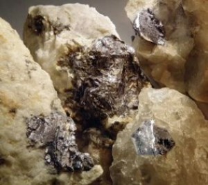
Molybdenum disulfide occurs in nature as molybdenite, crystalline material that frequently takes the characteristic form of silver-colored hexagonal plates. (Source: FUW)

Molybdenum disulfide occurs in nature as molybdenite, crystalline material that frequently takes the characteristic form of silver-colored hexagonal plates. (Source: FUW)

I am not able to find the published research at this time (March 13, 2014).

The tungsten diselenide story is specifically application-centric. Dexter Johnson in a March 11, 2014 post on his Nanoclast blog (on the IEEE [Institute of Electrical and Electronics Engineers] website) describes the differing perspectives and potential applications suggested by the three teams that cooperated to produce papers united by a joint theme ,

The three research groups focused on optoelectronics applications of tungsten diselenide, but each with a slightly different emphasis.

The University of Washington scientists highlighted applications of the material for a light emitting diode (LED). The Vienna University of Technology group focused on the material’s photovoltaic applications. And, finally, the MIT [Massachusetts Institute of Technology] group looked at all of the optoelectronic applications for the material that would result from the way it can be switched from being a p-type to a n-type semiconductor.

Here are some details of the research from each of the institutions’ news releases.

A March 10, 2014 University of Washington (state) news release highlights their LED work,

University of Washington [UW] scientists have built the thinnest-known LED that can be used as a source of light energy in electronics. The LED is based off of two-dimensional, flexible semiconductors, making it possible to stack or use in much smaller and more diverse applications than current technology allows.

“We are able to make the thinnest-possible LEDs, only three atoms thick yet mechanically strong. Such thin and foldable LEDs are critical for future portable and integrated electronic devices,” said Xiaodong Xu, a UW assistant professor in materials science and engineering and in physics.

The UW’s LED is made from flat sheets of the molecular semiconductor known as tungsten diselenide, a member of a group of two-dimensional materials that have been recently identified as the thinnest-known semiconductors. Researchers use regular adhesive tape to extract a single sheet of this material from thick, layered pieces in a method inspired by the 2010 Nobel Prize in Physics awarded to the University of Manchester for isolating one-atom-thick flakes of carbon, called graphene, from a piece of graphite.

In addition to light-emitting applications, this technology could open doors for using light as interconnects to run nano-scale computer chips instead of standard devices that operate off the movement of electrons, or electricity. The latter process creates a lot of heat and wastes power, whereas sending light through a chip to achieve the same purpose would be highly efficient.

“A promising solution is to replace the electrical interconnect with optical ones, which will maintain the high bandwidth but consume less energy,” Xu said. “Our work makes it possible to make highly integrated and energy-efficient devices in areas such as lighting, optical communication and nano lasers.”

Here’s a link to and a citation for this team’s paper,

Electrically tunable excitonic light-emitting diodes based on monolayer WSe2 p–n junctions by Jason S. Ross, Philip Klement, Aaron M. Jones, Nirmal J. Ghimire, Jiaqiang Yan, D. G. Mandrus, Takashi Taniguchi, Kenji Watanabe, Kenji Kitamura, Wang Yao, David H. Cobden, & Xiaodong Xu. Nature Nanotechnology (2014) doi:10.1038/nnano.2014.26 Published online 09 March 2014

This paper is behind a paywall.

A March 9, 2014 University of Vienna news release highlights their work on tungsten diselinide and its possible application in solar cells,

… With graphene as a light detector, optical signals can be transformed into electric pulses on extremely short timescales.

For one very similar application, however, graphene is not well suited for building solar cells. “The electronic states in graphene are not very practical for creating photovoltaics”, says Thomas Mueller. Therefore, he and his team started to look for other materials, which, similarly to graphene, can arranged in ultrathin layers, but have even better electronic properties.

The material of choice was tungsten diselenide: It consists of one layer of tungsten atoms, which are connected by selenium atoms above and below the tungsten plane. The material absorbs light, much like graphene, but in tungsten diselenide, this light can be used to create electrical power.

The layer is so thin that 95% of the light just passes through – but a tenth of the remaining five percent, which are absorbed by the material, are converted into electrical power. Therefore, the internal efficiency is quite high. A larger portion of the incident light can be used if several of the ultrathin layers are stacked on top of each other – but sometimes the high transparency can be a useful side effect. “We are envisioning solar cell layers on glass facades, which let part of the light into the building while at the same time creating electricity”, says Thomas Mueller.

Today, standard solar cells are mostly made of silicon, they are rather bulky and inflexible. Organic materials are also used for opto-electronic applications, but they age rather quickly. “A big advantage of two-dimensional structures of single atomic layers is their crystallinity. Crystal structures lend stability”, says Thomas Mueller.

Here’s a link to and a citation for the University of Vienna paper,

Solar-energy conversion and light emission in an atomic monolayer p–n diode by Andreas Pospischil, Marco M. Furchi, & Thomas Mueller. Nature Nanotechnology (2014) doi:10.1038/nnano.2014.14 Published online 09 March 2014

This paper is behind a paywll.

Finally, a March 10, 2014 MIT news release details their work about material able to switch from p-type (p = positive) to a n-type (n = negative) semiconductors,

The material they used, called tungsten diselenide (WSe2), is part of a class of single-molecule-thick materials under investigation for possible use in new optoelectronic devices — ones that can manipulate the interactions of light and electricity. In these experiments, the MIT researchers were able to use the material to produce diodes, the basic building block of modern electronics.

Typically, diodes (which allow electrons to flow in only one direction) are made by “doping,” which is a process of injecting other atoms into the crystal structure of a host material. By using different materials for this irreversible process, it is possible to make either of the two basic kinds of semiconducting materials, p-type or n-type.

But with the new material, either p-type or n-type functions can be obtained just by bringing the vanishingly thin film into very close proximity with an adjacent metal electrode, and tuning the voltage in this electrode from positive to negative. That means the material can easily and instantly be switched from one type to the other, which is rarely the case with conventional semiconductors.

In their experiments, the MIT team produced a device with a sheet of WSe2 material that was electrically doped half n-type and half p-type, creating a working diode that has properties “very close to the ideal,” Jarillo-Herrero says.

By making diodes, it is possible to produce all three basic optoelectronic devices — photodetectors, photovoltaic cells, and LEDs; the MIT team has demonstrated all three, Jarillo-Herrero says. While these are proof-of-concept devices, and not designed for scaling up, the successful demonstration could point the way toward a wide range of potential uses, he says.

“It’s known how to make very large-area materials” of this type, Churchill says. While further work will be required, he says, “there’s no reason you wouldn’t be able to do it on an industrial scale.”

In principle, Jarillo-Herrero says, because this material can be engineered to produce different values of a key property called bandgap, it should be possible to make LEDs that produce any color — something that is difficult to do with conventional materials. And because the material is so thin, transparent, and lightweight, devices such as solar cells or displays could potentially be built into building or vehicle windows, or even incorporated into clothing, he says.

While selenium is not as abundant as silicon or other promising materials for electronics, the thinness of these sheets is a big advantage, Churchill points out: “It’s thousands or tens of thousands of times thinner” than conventional diode materials, “so you’d use thousands of times less material” to make devices of a given size.

Here’s a link to and a citation for the MIT paper,

Optoelectronic devices based on electrically tunable p–n diodes in a monolayer dichalcogenide by Britton W. H. Baugher, Hugh O. H. Churchill, Yafang Yang, & Pablo Jarillo-Herrero. Nature Nanotechnology (2014) doi:10.1038/nnano.2014.25 Published online 09 March 2014

This paper is behind a paywall.

These are very exciting, if not to say, electrifying times. (Couldn’t resist the wordplay.)