Tag Archives: Dexter Johnson

UK’s National Graphene Institute kerfuffle gets bigger

First mentioned here in a March 18, 2016 posting titled: Tempest in a teapot or a sign of things to come? UK’s National Graphene Institute kerfuffle, the ‘scandal’ seems to be getting bigger, from a March 29, 2016 posting on Dexter Johnson’s Nanoclast blog on the IEEE (Institute of Electrical and Electronics Engineers) website (Note: A link has been removed),

Since that news story broke, damage control from the NGI [UK National Graphene Institute], the University of Manchester, and BGT Materials, the company identified in the Times article, has been coming fast and furious. Even this blog’s coverage of the story has gotten comments from representatives of BGT Materials and the University of Manchester.

There was perhaps no greater effort in this coordinated defense than getting Andre Geim, a University of Manchester researcher who was a co-discoverer of graphene, to weigh in. …

Despite Geim’s recent public defense, and a full-on PR campaign to turn around the perception that the UK government was investing millions into UK research only to have the fruits of that research sold off to foreign interests, there was news last week that the UK Parliament would be launching an inquiry into the “benefits and disbenefits of the way that graphene’s intellectual property and commercialisation has been managed, including through research and innovation collaborations.”

The timing for the inquiry is intriguing but there have been no public comments or hints that the NGI kerfuffle precipitated the Graphene Inquiry,

The Science and Technology Committee issues a call for written submissions for its inquiry on graphene.

Send written submissions

The inquiry explores the lessons from graphene for research and innovation in other areas, as well as the management and commercialisation of graphene’s intellectual property. Issues include:

  • The research obstacles that have had to be overcome for graphene, including identifying research priorities and securing research funding, and the lessons from this for other areas of research.
  • The factors that have contributed to the successful development of graphene and how these might be applied in other areas, including translating research into innovation, managing/sharing intellectual property, securing development funding, and bringing key stakeholders together.
  • The benefits and disbenefits of the way that graphene’s intellectual property and commercialisation has been managed, including through research and innovation collaborations, and the lessons from this for other areas.

The deadline for submissions is midday on Monday 18 April 2016.

The Committee expects to take oral evidence later in April 2016.

Getting back to the NGI, BGT Materials, and University of Manchester situation, there’s a forceful comment from Daniel Cochlin (identified as a graphene communications and marketing manager at the University of Manchester in an April 2, 2015 posting on Nanoclast) in Dexter’s latest posting about the NGI. From the comments section of a March 29, 2016 posting on the Nanoclast blog,

Maybe the best way to respond is to directly counter some of your assertions.

1. The NGI’s comments on this blog were to counter factual inaccuracies contained in your story. Your Editor-in-Chief and Editorial Director, Digital were also emailed to complain about the story, with not so much as an acknowledgement of the email.
2. There was categorically no ‘coaxing’ of Sir Andre to make comments. He was motivated to by the inaccuracies and insinuations of the Sunday Times article.
3. Members of the Science and Technology Select Committee visited the NGI about ten days before the Sunday Times article and this was followed by their desire to hold an evidence session to discuss graphene commercialisation.
4. The matter of how many researchers work in the NGI is not ‘hotly contested’. The NGI is 75% full with around 130 researchers regularly working there. We would expect this figure to grow by 10-15% within the next few days as other facilities are closed down.
5. Graphene Lighting PLC is the spin-out company set up to produce and market the lightbulb. To describe them as a ‘shadowy spin-out’ is unjustified and, I would suggest, libelous [emphasis mine].
6. Your question about why, if BGT Materials is a UK company, was it not mentioned [emphasis mine] in connection with the lightbulb is confusing – as stated earlier the company set up to manage the lightbulb was Graphene Lighting PLC.

Let’s hope it doesn’t take three days for this to be accepted by your moderators, as it did last time.

*ETA March 31, 2016 at 1530 hours PDT: Dexter has posted response comments in answer to Cochlin’s. You can read them for youself here .* I have a couple of observations (1) The use of the word ‘libelous’ seems a bit over the top. However, it should be noted that it’s much easier to sue someone for libel in England where the University of Manchester is located than it is in most jurisdictions. In fact, there’s an industry known as ‘libel tourism’ where litigious companies and individuals shop around for a jurisdiction such as England where they can easily file suit. (2) As for BGT Materials not being mentioned in the 2015 press release for the graphene lightbulb, I cannot emphasize how unusual that is. Generally speaking, everyone and every agency that had any involvement in developing and bringing to market a new product, especially one that was the ‘first consumer graphene-based product’, is mentioned. When you consider that BGT Materials is a newish company according to its About page,

BGT Materials Limited (BGT), established in 2013, is dedicated to the development of graphene technologies that utilize this “wonder material” to enhance our lives. BGT has pioneered the mass production of large-area, high-quality graphene rapidly achieving the first milestone required for the commercialization of graphene-enhanced applications.

the situation grows more peculiar. A new company wants and needs that kind of exposure to attract investment and/or keep current stakeholders happy. One last comment about BGT Materials and its public relations, Thanasis Georgiou, VP BGT Materials, Visiting scientist at the University of Manchester (more can be found on his website’s About page), waded into the comments section of Dexter’s March 15, 2016 posting and the first about the kerfuffle. Gheorgiou starts out in a relatively friendly fashion but his followup has a sharper tone,

I appreciate your position but a simple email to us and we would clarify most of the issues that you raised. Indeed your article carries the same inaccuracies that the initial Sunday Times article does, which is currently the subject of a legal claim by BGT Materials. [emphasis mine]

For example, BGT Materials is a UK registered company, not a Taiwanese one. A quick google search and you can confirm this. There was no “shadowy Canadian investor”, the company went through a round of financing, as most technology startups do, in order to reach the market quickly.

It’s hard to tell if Gheorgiou is trying to inform Dexter or threaten him in his comment to the March 15, 2016 posting but taken together with Daniel Cochlin’s claim of libel in his comment to the March 29, 2016 posting, it suggests an attempt at intimidation.

These are understandable responses given the stakes involved but moving to the most damaging munitions in your arsenal is usually not a good choice for your first  or second response.
Tempest in a teapot or a sign of things to come? UK’s National Graphene Institute kerfuffle

A scandal-in-the-offing, intellectual property, miffed academics, a chortling businessman, graphene, and much more make this a fascinating story.

Before launching into the main attractions, those unfamiliar with the UK graphene effort might find this background informal useful. Graphene, was first isolated at the University of Manchester in 2004 by scientists Andre Geim* and Konstantin Novoselov, Russian immigrants, both of whom have since become Nobel laureates and knights of the realm. The excitement in the UK and elsewhere is due to graphene’s extraordinary properties which could lead to transparent electronics, foldable/bendable electronics, better implants, efficient and inexpensive (they hope) water filters, and more. The UK government has invested a lot of money in graphene as has the European Union (1B Euros in the Graphene Flagship) in the hope that huge economic benefits will be reaped.

Dexter Johnson’s March 15, 2016 posting on his Nanoclast blog (on the IEEE [Institute for Electrical and Electronics Engineers] website) provides details about the situation (Note: Links have been removed),

A technology that, a year ago, was being lauded as the “first commercially viable consumer product” using graphene now appears to be caught up in an imbroglio over who owns its intellectual property rights. The resulting controversy has left the research institute behind the technology in a bit of a public relations quagmire.

The venerable UK publication The Sunday Times reported this week on what appeared to be a mutiny occurring at the National Graphene Institute (NGI) located at the University of Manchester. Researchers at the NGI had reportedly stayed away from working at the institute’s gleaming new $71 million research facility over fears that their research was going to end up in the hands of foreign companies, in particular a Taiwan-based company called BGT Materials.

The “first commercially viable consumer product” noted in Dexter’s posting was a graphene-based lightbulb which was announced by the NGI to much loud crowing in March 2015 (see my March 30, 2015 posting). The company producing the lightbulb was announced as “… Graphene Lighting PLC is a spin-out based on a strategic partnership with the National Graphene Institute (NGI) at The University of Manchester to create graphene applications.” There was no mention of BGT.

Dexter describes the situation from the BGT perspective (from his March 15, 2016 posting), Note: Links have been removed,

… BGT did not demur when asked by  the Times whether it owned the technology. In fact, Chung Ping Lai, BGT’s CEO, claimed it was his company that had invented the technology for the light bulb and not the NGI. The Times report further stated that Lai controls all the key patents and claims to be delighted with his joint venture with the university. “I believe in luck and I have had luck in Manchester,” Lai told the Times.

With companies outside the UK holding majority stakes in the companies spun out of the NGI—allowing them to claim ownership of the technologies developed at the institute—one is left to wonder what was the purpose of the £50 million (US $79 million) earmarked for graphene research in the UK more than four years ago? Was it to develop a local economy based around graphene—a “Graphene Valley”, if you will? Or was it to prop up the local construction industry through the building of shiny new buildings that reportedly few people occupy? That’s the charge leveled by Andre Geim, Nobel laureate for his discovery of graphene, and NGI’s shining star. Geim reportedly described the new NGI building as: “Money put in the British building industry rather than science.”

Dexter ends his March 15, 2016 posting with an observation  that will seem familiar to Canadians,

Now, it seems the government’s eagerness to invest in graphene research—or at least, the facilities for conducting that research—might have ended up bringing it to the same place as its previous lack of investment: the science is done in the UK and the exploitation of the technology is done elsewhere.

The March 13, 2016 Sunday Times article [ETA on April 3, 2016: This article is now behind a paywall] by Tom Harper, Jon Ungoed-Thomas and Michael Sheridan, which seems to be the source of Dexter’s posting, takes a more partisan approach,

ACADEMICS are boycotting a top research facility after a company linked to China was given access to lucrative confidential material from one of Britain’s greatest scientific breakthroughs.

Some scientists at Manchester University working on graphene, a wonder substance 200 times stronger than steel, refuse to work at the new £61m national institution, set up to find ways to exploit the material, amid concerns over a deal struck between senior university management and BGT Materials.

The academics are concerned that the National Graphene Institute (NGI), which was opened last year by George Osborne, the chancellor, and forms one of the key planks of his “northern powerhouse” industrial strategy, does not have the necessary safeguards to protect their confidential research, which could revolutionise the electronics, energy, health and building industries.

BGT, which is controlled by a Taiwanese businessman, subsequently agreed to work with a Chinese manufacturing company and university to develop similar graphene technology.

BGT says its work in Manchester has been successful and it is “offensive” and “untrue” to suggest that it would unfairly use intellectual property. The university say there is no evidence “whatsoever” of unfair use of confidential information. Manchester says it is understandable that some scientists are cautious about the collaborative environment of the new institute. But one senior academic said the arrangement with BGT had caused the university’s graphene research to descend into “complete anarchy”.

The academic said: “The NGI is a national facility, and why should we use it for a company, which is not even an English [owned] company? How much [intellectual property] is staying in England and how much is going to Taiwan?”

The row highlights concerns that the UK has dawdled in developing one of its greatest discoveries. Nearly 50% of ­graphene-related patents have been filed in China, and just 1% in Britain.

Manchester signed a £5m “research collaboration agreement” with BGT Materials in October 2013. Although the company is controlled by a Taiwanese businessman, Chung-ping Lai, the university does have a 17.5% shareholding.

Manchester claimed that the commercial deal would “attract a significant number of jobs to the city” and “benefit the UK economy”.

However, an investigation by The Sunday Times has established:

Only four jobs have been created as a result of the deal and BGT has not paid the full £5m due under the agreement after two projects were cancelled.

Pictures sent to The Sunday Times by a source at the university last month show that the offices at the NGI [National Graphene Institute], which can accommodate 120 staff, were deserted.

British-based businessmen working with graphene have also told The Sunday Times of their concerns about the institute’s information security. Tim Harper, a Manchester-based graphene entrepreneur, said: “We looked at locating there [at the NGI] but we take intellectual property extremely seriously and it is a problem locating in such a facility.

“If you don’t have control over your computer systems or the keys to your lab, then you’ve got a problem.”

I recommend reading Dexter’s post and the Sunday Times article as they provide some compelling insight into the UK situation vis à vis nanotechnology, science, and innovation.

*’Gheim’ corrected to ‘Geim’ on March 30, 2016.

Portable graphene-based supercapacitor comes to market soon

Dexter Johnson’s excitement is palpable in a Feb. 25, 2016 posting (on his Nanoclast blog on the IEEE [Institute for Electrical and Electronics Engineers] website) about a graphene-based supercapacitor,

At long last, there is a company that is about to launch a commercially available product based on a graphene-enabled supercapacitor. A UK-based startup called Zap&Go has found a way to exploit the attractive properties of graphene for supercapactiors to fabricate a portable charger and expects to make it available to consumers this year.

While graphene’s theoretical surface area of 2630 square meters per gram is pretty high, and would presumably bode well for increased capacity, this density is only possible with a single, standalone graphene sheet. And therein lies the rub: you can’t actually use a standalone sheet for the electrode of a supercapacitor because it will result in a very low volumetric capacitance. To get to a real-world device, you have to stack the sheets on top of each other. When you do this, the surface area is reduced.

Nonetheless graphene does have two main benefits going for it in supercapacitors: its ability to be structured into smaller sizes and its high conductance.

It is these qualities that Zap&Go have exploited for their portable charger. While there are other rechargers on the market, they are built around Li-ion batteries that take a long time to charge up and still present some small danger when packed up for traveling.

While your devices will still take just as long to charge, there are some compelling benefits,

You can find out more in Dexter’s posting, or on Zap&Go’s website, or on the company’s IndieGoGo crowdfunding campaign page (it’s closed and they more than reached their goal).

The charger is available for pre-ordering and will be delivered in Summer 2016, according to the company’s website store.

One final comment, I’m not endorsing this product, in other words, caveat emptor (buyer beware).

Australians take step toward ‘smart’ contact lenses

Some research from RMIT University (Australia) and the University of Adelaide (Australia) is make quite an impression. A Feb. 19, 2016 article by Caleb Radford for The Lead explains some of the excitement,

NEW light-manipulating nano-technology may soon be used to make smart contact lenses.

The University of Adelaide in South Australia worked closely with RMIT University to develop small hi-tech lenses to filter harmful optical radiation without distorting vision.

Dr Withawat Withayachumnankul from the University of Adelaide helped conceive the idea and said the potential applications of the technology included creating new high-performance devices that connect to the Internet.

A Feb. 19, 2016 RMIT University press release on EurekAlert, which originated the news item, provides more detail,

The light manipulation relies on creating tiny artificial crystals termed “dielectric resonators”, which are a fraction of the wavelength of light – 100-200 nanometers, or over 500 times thinner than a human hair.

The research combined the University of Adelaide researchers’ expertise in interaction of light with artificial materials with the materials science and nanofabrication expertise at RMIT University.

Dr Withawat Withayachumnankul, from the University of Adelaide’s School of Electrical and Electronic Engineering, said: “Manipulation of light using these artificial crystals uses precise engineering.

“With advanced techniques to control the properties of surfaces, we can dynamically control their filter properties, which allow us to potentially create devices for high data-rate optical communication or smart contact lenses.

“The current challenge is that dielectric resonators only work for specific colours, but with our flexible surface we can adjust the operation range simply by stretching it.”

Associate Professor Madhu Bhaskaran, Co-Leader of the Functional Materials and Microsystems Research Group at RMIT, said the devices were made on a rubber-like material used for contact lenses.

“We embed precisely-controlled crystals of titanium oxide, a material that is usually found in sunscreen, in these soft and pliable materials,” she said.

“Both materials are proven to be bio-compatible, forming an ideal platform for wearable optical devices.

“By engineering the shape of these common materials, we can create a device that changes properties when stretched. This modifies the way the light interacts with and travels through the device, which holds promise of making smart contact lenses and stretchable colour changing surfaces.”

Lead author and RMIT researcher Dr. Philipp Gutruf said the major scientific hurdle overcome by the team was combining high temperature processed titanium dioxide with the rubber-like material, and achieving nanoscale features.

“With this technology, we now have the ability to develop light weight wearable optical components which also allow for the creation of futuristic devices such as smart contact lenses or flexible ultra thin smartphone cameras,” Gutruf said.

Here’s a link to and a citation for the paper,

Mechanically Tunable Dielectric Resonator Metasurfaces at Visible Frequencies by Philipp Gutruf, Chengjun Zou, Withawat Withayachumnankul, Madhu Bhaskaran, Sharath Sriram, and Christophe Fumeaux. ACS Nano, 2016, 10 (1), pp 133–141 DOI: 10.1021/acsnano.5b05954 Publication Date (Web): November 30, 2015

Copyright © 2015 American Chemical Society

This paper is behind a paywall.

ETA Feb. 24, 2016: Dexter Johnson (Nanoclast blog on the IEEE [Institute of Electrical and Electronics Engineers] website) has chimed in with additional insight into this research in his Feb. 23, 2016 posting.

Plasmonic interferometry without coherent light

There are already a number of biosensors based on plasmonic interferometry in use but this latest breakthrough from Brown University (US) could make them cheaper and more accessible. A Feb. 16, 2016 Brown University news release (also on EurekAlert), announces the new technique,

Imagine a hand-held environmental sensor that can instantly test water for lead, E. coli, and pesticides all at the same time, or a biosensor that can perform a complete blood workup from just a single drop. That’s the promise of nanoscale plasmonic interferometry, a technique that combines nanotechnology with plasmonics–the interaction between electrons in a metal and light.

Now researchers from Brown University’s School of Engineering have made an important fundamental advance that could make such devices more practical. The research team has developed a technique that eliminates the need for highly specialized external light sources that deliver coherent light, which the technique normally requires. The advance could enable more versatile and more compact devices.

“It has always been assumed that coherent light was necessary for plasmonic interferometry,” said Domenico Pacifici, a professor of engineering who oversaw the work with his postdoctoral researcher Dongfang Li, and graduate student Jing Feng. “But we were able to disprove that assumption.”

The research is described in Nature Scientific Reports.

Plasmonic interferometers make use of the interaction between light and surface plasmon polaritons, density waves created when light energy rattles free electrons in a metal. One type of interferometer looks like a bull’s-eye structure etched into a thin layer of metal. In the center is a hole poked through the metal layer with a diameter of about 300 nanometers–about 1,000 times smaller than the diameter of a human hair. The hole is encircled by a series of etched grooves, with diameters of a few micrometers. Thousands of these bulls-eyes can be placed on a chip the size of a fingernail.

When light from an external source is shown onto the surface of an interferometer, some of the photons go through the central hole, while others are scattered by the grooves. Those scattered photons generate surface plasmons that propagate through the metal inward toward the hole, where they interact with photons passing through the hole. That creates an interference pattern in the light emitted from the hole, which can be recorded by a detector beneath the metal surface.

When a liquid is deposited on top of an interferometer, the light and the surface plasmons propagate through that liquid before they interfere with each other. That alters the interference patterns picked up by the detector depending on the chemical makeup of the liquid or compounds present in it. By using different sizes of groove rings around the hole, the interferometers can be tuned to detect the signature of specific compounds or molecules. With the ability to put many differently tuned interferometers on one chip, engineers can hypothetically make a versatile detector.

Up to now, all plasmonic interferometers have required the use of highly specialized external light sources that can deliver coherent light–beams in which light waves are parallel, have the same wavelength, and travel in-phase (meaning the peaks and valleys of the waves are aligned). Without coherent light sources, the interferometers cannot produce usable interference patterns. Those kinds of light sources, however, tend to be bulky, expensive, and require careful alignment and periodic recalibration to obtain a reliable optical response.

But Pacifici and his group have come up with a way to eliminate the need for external coherent light. In the new method, fluorescent light-emitting atoms are integrated directly within the tiny hole in the center of the interferometer. An external light source is still necessary to excite the internal emitters, but it need not be a specialized coherent source.

“This is a whole new concept for optical interferometry,” Pacifici said, “an entirely new device.”

In this new device, incoherent light shown on the interferometer causes the fluorescent atoms inside the center hole to generate surface plasmons. Those plasmons propagate outward from the hole, bounce off the groove rings, and propagate back toward the hole after. Once a plasmon propagates back, it interacts with the atom that released it, causing an interference with the directly transmitted photon. Because the emission of a photon and the generation of a plasmon are indistinguishable, alternative paths originating from the same emitter, the process is naturally coherent and interference can therefore occur even though the emitters are excited incoherently.

“The important thing here is that this is a self-interference process,” Pacifici said. “It doesn’t matter that you’re using incoherent light to excite the emitters, you still get a coherent process.”

In addition to eliminating the need for specialized external light sources, the approach has several advantages, Pacifici said. Because the surface plasmons travel out from the hole and back again, they probe the sample on top of the interferometer surface twice. That makes the device more sensitive.

But that’s not the only advantage. In the new device, external light can be projected from underneath the metal surface containing the interferometers instead of from above. That eliminates the need for complex illumination architectures on top of the sensing surface, which could make for easier integration into compact devices.

The embedded light emitters also eliminate the need to control the amount of sample liquid deposited on the interferometer’s surface. Large droplets of liquid can cause lensing effects, a bending of light that can scramble the results from the interferometer. Most plasmonic sensors make use of tiny microfluidic channels to deliver a thin film of liquid to avoid lensing problems. But with internal light emitters excited from the bottom surface, the external light never comes in contact with the sample, so lensing effects are negated, as is the need for microfluidics.

Finally, the internal emitters produce a low intensity light. That’s good for probing delicate samples, such as proteins, than can be damaged by high-intensity light.

More work is required to get the system out of the lab and into devices, and Pacifici and his team plan to continue to refine the idea. The next step will be to try eliminating the external light source altogether. It might be possible, the researchers say, to eventually excite the internal emitters using tiny fiber optic lines, or perhaps electric current.

Still, this initial proof-of-concept is promising, Pacifici said.

“From a fundamental standpoint, we think this new device represents a significant step forward,” he said, “a first demonstration of plasmonic interferometry with incoherent light”.

Here’s a link to and a citation for the paper,

Nanoscale optical interferometry with incoherent light by Dongfang Li, Jing Feng, & Domenico Pacifici. Scientific Reports 6, Article number: 20836 (2016) doi:10.1038/srep20836 Published online: 16 February 2016

This paper is open access.

One final comment, Dexter Johnson has a Feb. 18, 2016 posting about this interferometer where he references Pacifici’s past work in this area, as well as, this latest breakthrough. Dexter’s posting can be found on his Nanoclast blog which is on the IEEE (Institute of Electrical and Electronics Engineers) website.

University of Alberta team may open door to flexible electronics with engineering breakthrough

There’s some exciting news from the University of Alberta. It emerges from a team that has reconsidered transistor architecture, from a Feb. 9, 2016 news item on ScienceDaily,

An engineering research team at the University of Alberta has invented a new transistor that could revolutionize thin-film electronic devices.

The team was exploring new uses for thin film transistors (TFT), which are most commonly found in low-power, low-frequency devices like the display screen you’re reading from now. Efforts by researchers and the consumer electronics industry to improve the performance of the transistors have been slowed by the challenges of developing new materials or slowly improving existing ones for use in traditional thin film transistor architecture, known technically as the metal oxide semiconductor field effect transistor (MOSFET).

But the U of A electrical engineering team did a run-around on the problem. Instead of developing new materials, the researchers improved performance by designing a new transistor architecture that takes advantage of a bipolar action. In other words, instead of using one type of charge carrier, as most thin film transistors do, it uses electrons and the absence of electrons (referred to as “holes”) to contribute to electrical output. Their first breakthrough was forming an ‘inversion’ hole layer in a ‘wide-bandgap’ semiconductor, which has been a great challenge in the solid-state electronics field.

A Feb. 9, 2016 University of Alberta news release by Richard Cairney and Grecia Pacheco (also on EurekAlert), which originated the news item, provides more detail about the research,

Once this was achieved, “we were able to construct a unique combination of semiconductor and insulating layers that allowed us to inject “holes” at the MOS interface,” said Gem Shoute, a PhD student in the Department of Electrical and Computer Engineering who is lead author on the article. Adding holes at the interface increased the chances of an electron “tunneling” across a dielectric barrier. Through this phenomenon, a type of quantum tunnelling, “we were finally able to achieve a transistor that behaves like a bipolar transistor.”

“It’s actually the best performing [TFT] device of its kind–ever,” said materials engineering professor Ken Cadien, a co-author on the paper. “This kind of device is normally limited by the non-crystalline nature of the material that they are made of”

The dimension of the device itself can be scaled with ease in order to improve performance and keep up with the need of miniaturization, an advantage that modern TFTs lack. The transistor has power-handling capabilities at least 10 times greater than commercially produced thin film transistors.

Electrical engineering professor Doug Barlage, who is Shoute’s PhD supervisor and one of the paper’s lead authors, says his group was determined to try new approaches and break new ground. He says the team knew it could produce a high-power thin film transistor–it was just a matter of finding out how.

“Our goal was to make a thin film transistor with the highest power handling and switching speed possible. Not many people want to look into that, but the raw properties of the film indicated dramatic performance increase was within reach,” he said. “The high quality sub 30 nanometre (a human hair is 50,000 nanometres wide) layers of materials produced by Professor Cadien’s group enabled us to successfully try these difficult concepts”

In the end, the team took advantage of the very phenomena other researchers considered roadblocks.

“Usually tunnelling current is considered a bad thing in MOSFETs and it contributes to unnecessary loss of power, which manifests as heat,” explained Shoute. “What we’ve done is build a transistor that considers tunnelling current a benefit.”

Here’s a link to and a citation for the paper,

Sustained hole inversion layer in a wide-bandgap metal-oxide semiconductor with enhanced tunnel current by Gem Shoute, Amir Afshar, Triratna Muneshwar, Kenneth Cadien, & Douglas Barlage. Nature Communications 7, Article number: 10632 doi:10.1038/ncomms10632 Published 04 February 2016

This is an open access paper.

ETA Feb. 12, 2016: Dexter Johnson has written up the research in a Feb. 11, 2016 posting (on this Nanoclast blog on the IEEE [Institute of Electrical and Electronics Engineers) where he offers enthusiam (rare) and additional explanation.

Swinging from 2015 to 2016 with FrogHeart

On Thursday, Dec. 31, 2015, the bear ate me (borrowed from Joan Armatrading’s song “Eating the bear”) or, if you prefer this phrase, I had a meltdown when I lost more than 1/2 of a post that I’d worked on for hours.

There’s been a problem dogging me for some months. I will write up something and save it as a draft only to find that most of the text has been replaced by a single URL repeated several times. I have not been able to source the problem which is intermittent. (sigh)

Moving on to happier thoughts, it’s a new year. Happy 2016!

As a way of swinging into the new year, here’s a brief wrap up for 2015.

International colleagues

As always, I thank my international colleagues David Bruggeman (Pasco Phronesis blog), Dexter Johnson (Nanoclast blog on the IEEE [International Electrical and Electronics Engineers website]), and Dr. Andrew Maynard (2020 science blog and Risk Innovation Laboratory at Arizona State University), all of whom have been blogging as long or longer than I have (FYI, FrogHeart began in April/May 2008). More importantly, they have been wonderful sources of information and inspiration.

In particular, David, thank you for keeping me up to date on the Canadian and international science policy situations. Also, darn you for scooping me on the Canadian science policy scene, on more than one occasion.

Dexter, thank you for all those tidbits about the science and the business of nanotechnology that you tuck into your curated blog. There’s always a revelation or two to be found in your writings.

Andrew, congratulations on your move to Arizona State University (from the University of Michigan Risk Science Center) where you are founding their Risk Innovation Lab.

While Andrew’s blog has become more focused on the topic of risk, Andrew continues to write about nanotechnology by extending the topic to emerging technologies.

In fact, I have a Dec. 3, 2015 post featuring a recent Nature article by Andrew on the occasion of the upcoming 2016 World Economic Forum in Davos. In it he discusses new approaches to risk as occasioned by the rise of emerging technologies such synthetic biology, nanotechnology, and more.

While Tim Harper, serial entrepreneur and scientist, is not actively blogging about nanotechnology these days, his writings do pop up in various places, notably on the Azonano website where he is listed as an expert, which he most assuredly is. His focus these days is in establishing graphene-based startups.

Moving on to another somewhat related topic. While no one else seems to be writing about nanotechnology as extensively as I do, there are many, many Canadian science bloggers.

Canadian colleagues

Thank you to Gregor Wolbring, ur Canadian science blogger and professor at the University of Calgary. His writing about human enhancement has become increasingly timely as we continue to introduce electronics onto and into our bodies. While he writes regularly, I don’t believe he’s blogging regularly. However, you can find out more about Gregor and his work  at  http://www.crds.org/research/faculty/Gregor_Wolbring2.shtml
or on his facebook page
https://www.facebook.com/GregorWolbring

Science Borealis (scroll down to get to the feeds), a Canadian science blog aggregator, is my main source of information on the Canadian scene. Thank you for my second Editors Pick award. In 2014 the award was in the Science in Society category and in 2015 it’s in the Engineering & Tech category (last item on the list).

While I haven’t yet heard about the results of Paige Jarreau’s and Science Borealis’ joint survey on the Canadian science blog readers (the reader doesn’t have to be Canadian but the science blog has to be), I was delighted to be asked and to participate. My Dec. 14, 2015 posting listed preliminary results,

They have compiled some preliminary results:

  • 21 bloggers + Science Borealis hosted the survey.
  • 523 respondents began the survey.
  • 338 respondents entered their email addresses to win a prize
  • 63% of 400 Respondents are not science bloggers
  • 56% of 402 Respondents describe themselves as scientists
  • 76% of 431 Respondents were not familiar with Science Borealis before taking the survey
  • 85% of 403 Respondents often, very often or always seek out science information online.
  • 59% of 402 Respondents rarely or never seek science content that is specifically Canadian
  • Of 400 Respondents, locations were: 35% Canada, 35% US, 30% Other.

And most of all, a heartfelt thank you to all who read this blog.

FrogHeart and 2015

There won’t be any statistics from the software packaged with my  hosting service (AWSTATS and Webalizer). Google and its efforts to minimize spam (or so it claims) had a devastating effect on my visit numbers. As I used those numbers as motivation, fantasizing that my readership was increasing, I had to find other means for motivation and am not quite sure how I did it but I upped publication to three posts per day (five-day week) throughout most of the year.

With 260 working days (roughly) in a year that would have meant a total of 780 posts. I’ve rounded that down to 700 posts to allow for days off and days where I didn’t manage three.

In 2015 I logged my 4000th post and substantially contributed to the Science Borealis 2015 output. In the editors’ Dec. 20, 2015 post,

… Science Borealis now boasts a membership of 122 blogs  — about a dozen up from last year. Together, this year, our members have posted over 4,400 posts, with two weeks still to go….

At a rough guess, I’d estimate that FrogHeart was responsible for 15% of the Science Borealis output and 121 bloggers were responsible for the other 85%.

That’s enough for 2015.

FrogHeart and 2016

Bluntly, I do not know anything other than a change of some sort is likely.

Hopefully, I will be doing more art/science projects (my last one was ‘A digital poetry of gold nanoparticles’). I was awarded a small grant ($400 CAD) from the Canadian Academy of Independent Scholars (thank you!) for a spoken word project to be accomplished later this year.

As for this blog, I hope to continue.

In closing, I think it’s only fair to share Joan Armatrading’s song, ‘Eating the bear’. May we all do so in 2016,

Bonne Année!

The sound of moving data

In fact, scientists from the University of Sheffield (UK) and the University of Leeds (UK) have found a way to move data easily and quickly by using sound waves. From a Nov. 3, 2015 news item on ScienceDaily,

Nothing is more frustrating that watching that circle spinning in the centre of your screen, while you wait for your computer to load a programme or access the data you need. Now a team from the Universities of Sheffield and Leeds may have found the answer to faster computing: sound.

The research — published in Applied Physics Letters — has shown that certain types of sound waves can move data quickly, using minimal power.

A Nov. 3, 2015 University of Sheffield news release on EurekAlert, which originated the news item, explains some of the issues with data and memory before briefly describing how sound waves could provide a solution,

The world’s 2.7 zettabytes (2.7 followed by 21 zeros) of data are mostly held on hard disk drives: magnetic disks that work like miniaturised record players, with the data read by sensors that scan over the disk’s surface as it spins. But because this involves moving parts, there are limits on how fast it can operate.

For computers to run faster, we need to create “solid-state” drives that eliminate the need for moving parts – essentially making the data move, not the device on which it’s stored. Flash-based solid-state disk drives have achieved this, and store information electrically rather than magnetically. However, while they operate much faster than normal hard disks, they last much less time before becoming unreliable, are much more expensive and still run much slower than other parts of a modern computer – limiting total speed.

Creating a magnetic solid-state drive could overcome all of these problems. One solution being developed is ‘racetrack memory’, which uses tiny magnetic wires, each one hundreds of times thinner than a human hair, down which magnetic “bits” of data run like racing cars around a track. Existing research into racetrack memory has focused on using magnetic fields or electric currents to move the data bits down the wires. However, both these options create heat and reduce power efficiency, which will limit battery life, increase energy bills and CO2 emissions.

Dr Tom Hayward from the University of Sheffield and Professor John Cunningham from the University of Leeds have together come up with a completely new solution: passing sound waves across the surface on which the wires are fixed. They also found that the direction of data flow depends on the pitch of the sound generated – in effect they “sang” to the data to move it.

The sound used is in the form of surface acoustic waves – the same as the most destructive wave that can emanate from an earthquake. Although already harnessed for use in electronics and other areas of engineering, this is the first time surface acoustic waves have been applied to a data storage system.

Dr Hayward, from Sheffield’s Faculty of Engineering, said: “The key advantage of surface acoustic waves in this application is their ability to travel up to several centimetres without decaying, which at the nano-scale is a huge distance. Because of this, we think a single sound wave could be used to “sing” to large numbers of nanowires simultaneously, enabling us to move a lot of data using very little power. We’re now aiming to create prototype devices in which this concept can be fully tested.”

Here’s a link to and a citation for the paper,

A sound idea: Manipulating domain walls in magnetic nanowires using surface acoustic waves by J. Dean, M. T. Bryan, J. D. Cooper, A. Virbule, J. E. Cunningham, and T. J. Hayward. Appl. Phys. Lett. 107, 142405 (2015); http://dx.doi.org/10.1063/1.4932057

This is an open access paper.

Dexter Johnson in a Nov. 5, 2015 posting on his Nanoclast blog (on the IEEE [Institute of Electrical and Electronics Engineers] website) provides a few additional details about the work such as a brief mention of IBM’s work developing racetrack memory, also known as, a non-volatile memory device.

Touchless displays with 2D nanosheets and sweat

Swiping touchscreens with your finger has become a dominant means of accessing information in many applications but there is at least one problem associated with this action. From an Oct. 2, 2015 news item on phys.org,

While touchscreens are practical, touchless displays would be even more so. That’s because, despite touchscreens having enabled the smartphone’s advance into our lives and being essential for us to be able to use cash dispensers or ticket machines, they do have certain disadvantages. Touchscreens suffer from mechanical wear over time and are a transmission path for bacteria and viruses. To avoid these problems, scientists at Stuttgart’s Max Planck Institute for Solid State Research and LMU Munich have now developed nanostructures that change their electrical and even their optical properties as soon as a finger comes anywhere near them.

Here’s what a touchless screen looks like when tracking,

Touchless colour change: A nanostructure containing alternating layers of phosphatoantimonate nanosheets and oxide ... [more] © Advanced Materials 2015/MPI for Solid State Research

Touchless colour change: A nanostructure containing alternating layers of phosphatoantimonate nanosheets and oxide … [more]
© Advanced Materials 2015/MPI for Solid State Research

An Oct. 1, 2015 Max Planck Institute press release, which originated the news item, gives technical details,

A touchless display may be able to capitalize on a human trait which is of vital importance, although sometimes unwanted: This is the fact that our body sweats – and is constantly emitting water molecules through tiny pores in the skin. Scientists of the Nanochemistry group led by Bettina Lotsch at the Max Planck Institute for Solid State Research in Stuttgart and the LMU Munich have now been able to visualize the transpiration of a finger with a special moisture sensor which reacts as soon as an object – like an index finger – approaches its surface, without touching it. The increasing humidity is converted into an electrical signal or translated into a colour change, thus enabling it to be measured.

Phosphatoantimonic acid is what enables it to do this. This acid is a crystalline solid at room temperature with a structure made up of antimony, phosphorous, oxygen and hydrogen atoms. “It’s long been known to scientists that this material is able to take up water and swells considerably in the process,” explained Pirmin Ganter, doctoral student at the Max Planck Institute for Solid State Research and the Chemistry Department at LMU Munich. This water uptake also changes the properties of the material. For instance, its electrical conductivity increases as the number of stored water molecules rises. This is what enables it to serve as a measure of ambient moisture.

A sandwich nanomaterial structure exposed to moisture also changes its colour

However, the scientists aren’t so interested in developing a new moisture sensor. What they really want is to use it in touchless displays. “Because these sensors react in a very local manner to any increase in moisture, it is quite conceivable that this sort of material with moisture-dependent properties could also be used for touchless displays and monitors,” said Ganter. Touchless screens of this kind would require nothing more than a finger to get near the display to change their electrical or optical properties – and with them the input signal – at a specific point on the display.

Taking phosphatoantimonate nanosheets as their basis, the Stuttgart scientists then developed a photonic nanostructure which reacts to the moisture by changing colour. “If this was built into a monitor, the users would then receive visible feedback to  their finger motion” explained Katalin Szendrei, also a doctoral student in Bettina Lotsch’s group. To this end, the scientists created a multilayer sandwich material with alternating layers of ultrathin phosphatoantimonate nanosheets and silicon dioxide (SiO2) or titanium dioxide nanoparticles (TiO2). Comprising more than ten layers, the stack ultimately reached a height of little more than one millionth of a metre.

For one thing, the colour of the sandwich material can be set via the thickness of the layers. And for another, the colour of the sandwich changes if the scientists increase the relative humidity in the immediate surroundings of the material, for instance by moving a finger towards the screen. “The reason for this lies in the storage of water molecules between the phosphatoantimonate layers, which makes the layers swell considerably,” explained Katalin Szendrei. “A change in the thickness of the layers in this process is accompanied by a change in the colour of the sensor – produced in a similar way to what gives colour to a butterfly wing or in mother-of-pearl.”

The material reacts to the humidity change within a few milliseconds

This is a property that is fundamentally well known and characteristic of so-called photonic crystals. But scientists had never before observed such a large colour change as they now have in the lab in Stuttgart. “The colour of the nanostructure turns from blue to red when a finger gets near, for example. In this way, the colour can be tuned through the whole of the visible spectrum depending on the amount of water vapour taken up,” stressed Bettina Lotsch.

The scientists’ new approach is not only captivating because of the striking colour change. What’s also important is the fact that the material reacts to the change in humidity within a few milliseconds – literally in the blink of an eye. Previously reported materials normally took several seconds or more to respond. That is much too slow for practical applications. And there’s another thing that other materials couldn’t always do: The sandwich structure consisting of phosphatoantimonate nanosheets and oxide nanoparticles is highly stable from a chemical perspective and responds selectively to water vapour.

A layer protecting against chemical influences has to let moisture through

The scientists can imagine their materials being used in much more than just future generations of smartphones, tablets or notebooks. “Ultimately, we could see touchless displays also being deployed in many places where people currently have to touch monitors to navigate,” said Bettina Lotsch. For instance in cash dispensers or ticket machines, or even at the weighing scales in the supermarket’s vegetable aisle. Displays in public placesthat are used by many different people would have distinct hygiene benefits if they were touchless.

But before we see them being used in such places, the scientists have a few more challenges to overcome. It’s important, for example, that the nanostructures can be produced economically. To minimize wear, the structures still need to be coated with a protective layer if they’re going to be used in anything like a display. And that, again, has to meet not one but two different requirements: It must protect the moisture-sensitive layers against chemical and mechanical influences. And it must, of course, let the moisture pass through. But the Stuttgart scientists have an idea for how to achieve that already. An idea they are currently starting to put into practice with an additional cooperation partner on board.

Dexter Johnson’s Oct. 2, 2015 posting on his Nanoclast blog (on the IEEE [Institute of Electrical and Electronics Engineers] website) provides some additional context for this research (Note: A link has been removed),

In a world where the “swipe” has become a dominant computer interface method along with moving and clicking the mouse, the question becomes what’s next? For researchers at Stuttgart’s Max Planck Institute for Solid State Research and LMU Munich, Germany, the answer continues to be a swipe, but one in which you don’t actually need to touch the screen with your finger. Researchers call these no-contact computer screens touchless positioning interfaces (TPI).

Here’s a link to and a citation for the paper,

Touchless Optical Finger Motion Tracking Based on 2D Nanosheets with Giant Moisture Responsiveness by Katalin Szendrei, Pirmin Ganter, Olalla Sànchez-Sobrado, Roland Eger, Alexander Kuhn, and Bettina V. Lotsch. Advanced Materials DOI: 10.1002/adma.201503463 Article first published online: 22 SEP 2015

© 2015 WILEY-VCH Verlag GmbH & Co. KGaA, Weinheim

This paper is behind a paywall.

Cleaning up carbon dioxide pollution in the oceans and elsewhere

I have a mini roundup of items (3) concerning nanotechnology and environmental applications with a special focus on carbon materials.

Carbon-capturing motors

First up, there’s a Sept. 23, 2015 news item on ScienceDaily which describes work with tiny carbon-capturing motors,

Machines that are much smaller than the width of a human hair could one day help clean up carbon dioxide pollution in the oceans. Nanoengineers at the University of California, San Diego have designed enzyme-functionalized micromotors that rapidly zoom around in water, remove carbon dioxide and convert it into a usable solid form.

The proof of concept study represents a promising route to mitigate the buildup of carbon dioxide, a major greenhouse gas in the environment, said researchers. …

A Sept 22, 2015 University of California at San Diego (UCSD) news release by Liezel Labios, which originated the news release, provides more details about the scientists’ hopes and the technology,

“We’re excited about the possibility of using these micromotors to combat ocean acidification and global warming,” said Virendra V. Singh, a postdoctoral scientist in Wang’s [nanoengineering professor and chair Joseph Wang] research group and a co-first author of this study.

In their experiments, nanoengineers demonstrated that the micromotors rapidly decarbonated water solutions that were saturated with carbon dioxide. Within five minutes, the micromotors removed 90 percent of the carbon dioxide from a solution of deionized water. The micromotors were just as effective in a sea water solution and removed 88 percent of the carbon dioxide in the same timeframe.

“In the future, we could potentially use these micromotors as part of a water treatment system, like a water decarbonation plant,” said Kevin Kaufmann, an undergraduate researcher in Wang’s lab and a co-author of the study.

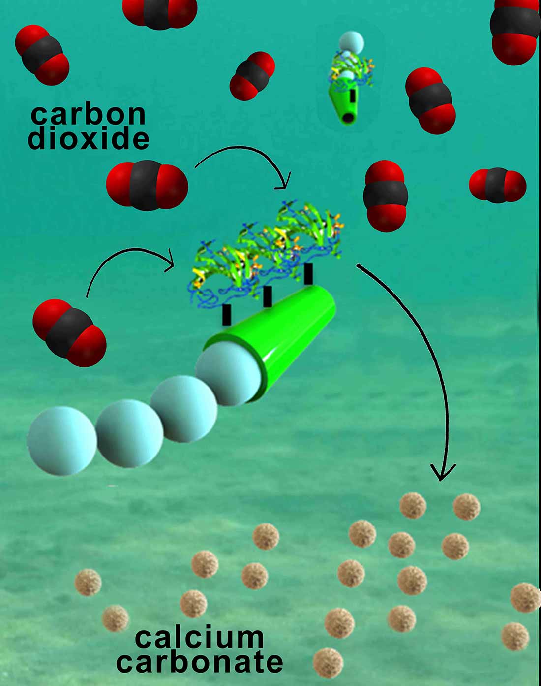
The micromotors are essentially six-micrometer-long tubes that help rapidly convert carbon dioxide into calcium carbonate, a solid mineral found in eggshells, the shells of various marine organisms, calcium supplements and cement. The micromotors have an outer polymer surface that holds the enzyme carbonic anhydrase, which speeds up the reaction between carbon dioxide and water to form bicarbonate. Calcium chloride, which is added to the water solutions, helps convert bicarbonate to calcium carbonate.

The fast and continuous motion of the micromotors in solution makes the micromotors extremely efficient at removing carbon dioxide from water, said researchers. The team explained that the micromotors’ autonomous movement induces efficient solution mixing, leading to faster carbon dioxide conversion. To fuel the micromotors in water, researchers added hydrogen peroxide, which reacts with the inner platinum surface of the micromotors to generate a stream of oxygen gas bubbles that propel the micromotors around. When released in water solutions containing as little as two to four percent hydrogen peroxide, the micromotors reached speeds of more than 100 micrometers per second.

However, the use of hydrogen peroxide as the micromotor fuel is a drawback because it is an extra additive and requires the use of expensive platinum materials to build the micromotors. As a next step, researchers are planning to make carbon-capturing micromotors that can be propelled by water.

“If the micromotors can use the environment as fuel, they will be more scalable, environmentally friendly and less expensive,” said Kaufmann.

The researchers have provided an image which illustrates the carbon-capturing motors in action,

Nanoengineers have invented tiny tube-shaped micromotors that zoom around in water and efficiently remove carbon dioxide. The surfaces of the micromotors are functionalized with the enzyme carbonic anhydrase, which enables the motors to help rapidly convert carbon dioxide to calcium carbonate. Image credit: Laboratory for Nanobioelectronics, UC San Diego Jacobs School of Engineering.

Nanoengineers have invented tiny tube-shaped micromotors that zoom around in water and efficiently remove carbon dioxide. The surfaces of the micromotors are functionalized with the enzyme carbonic anhydrase, which enables the motors to help rapidly convert carbon dioxide to calcium carbonate. Image credit: Laboratory for Nanobioelectronics, UC San Diego Jacobs School of Engineering.

Here’s a link to and a citation for the paper,

Micromotor-Based Biomimetic Carbon Dioxide Sequestration: Towards Mobile Microscrubbers by Murat Uygun, Virendra V. Singh, Kevin Kaufmann, Deniz A. Uygun, Severina D. S. de Oliveira, and oseph Wang. Angewandte Chemie DOI: 10.1002/ange.201505155 Article first published online: 4 SEP 2015

© 2015 WILEY-VCH Verlag GmbH & Co. KGaA, Weinheim

This article is behind a paywall.

Carbon nanotubes for carbon dioxide capture (carbon capture)

In a Sept. 22, 2015 posting by Dexter Johnson on his Nanoclast blog (located on the IEEE [Institute for Electrical and Electronics Engineers] website) describes research where carbon nanotubes are being used for carbon capture,

Now researchers at Technische Universität Darmstadt in Germany and the Indian Institute of Technology Kanpur have found that they can tailor the gas adsorption properties of vertically aligned carbon nanotubes (VACNTs) by altering their thickness, height, and the distance between them.

“These parameters are fundamental for ‘tuning’ the hierarchical pore structure of the VACNTs,” explained Mahshid Rahimi and Deepu Babu, doctoral students at the Technische Universität Darmstadt who were the paper’s lead authors, in a press release. “This hierarchy effect is a crucial factor for getting high-adsorption capacities as well as mass transport into the nanostructure. Surprisingly, from theory and by experiment, we found that the distance between nanotubes plays a much larger role in gas adsorption than the tube diameter does.”

Dexter provides a good and brief summary of the research.

Here’s a link to and a citation for the paper,

Double-walled carbon nanotube array for CO2 and SO2 adsorption by Mahshid Rahimi, Deepu J. Babu, Jayant K. Singh, Yong-Biao Yang, Jörg J. Schneider, and Florian Müller-Plathe. J. Chem. Phys. 143, 124701 (2015); http://dx.doi.org/10.1063/1.4929609

This paper is open access.

The market for nanotechnology-enabled environmental applications

Coincident with stumbling across these two possible capture solutions, I found this Sept. 23, 2015 BCC Research news release,

A groundswell of global support for developing nanotechnology as a pollution remediation technique will continue for the foreseeable future. BCC Research reveals in its new report that this key driver, along with increasing worldwide concerns over removing pollutants and developing alternative energy sources, will drive growth in the nanotechnology environmental applications market.

The global nanotechnology market in environmental applications is expected to reach $25.7 billion by 2015 and $41.8 billion by 2020, conforming to a five-year (2015-2020) compound annual growth rate (CAGR) of 10.2%. Air remediation as a segment will reach $10.2 billion and $16.7 billion in 2015 and 2020, respectively, reflecting a five-year CAGR of 10.3%. Water remediation as a segment will grow at a five-year CAGR of 12.4% to reach $10.6 billion in 2020.

As nanoparticles push the limits and capabilities of technology, new and better techniques for pollution control are emerging. Presently, nanotechnology’s greatest potential lies in air pollution remediation.

“Nano filters could be applied to automobile tailpipes and factory smokestacks to separate out contaminants and prevent them from entering the atmosphere. In addition, nano sensors have been developed to sense toxic gas leaks at extremely low concentrations,” says BCC research analyst Aneesh Kumar. “Overall, there is a multitude of promising environmental applications for nanotechnology, with the main focus area on energy and water technologies.”

You can find links to the report, TOC (table of contents), and report overview on the BCC Research Nanotechnology in Environmental Applications: The Global Market report webpage.