Tag Archives: organic electronics

Mimicking the brain with an evolvable organic electrochemical transistor

Simone Fabiano and Jennifer Gerasimov have developed a learning transistor that mimics the way synapses function. Credit: Thor Balkhed

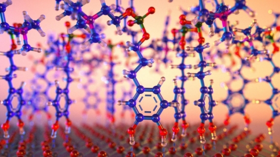
At a guess, this was originally a photograph which has been passed through some sort of programme to give it a paintinglike quality.

Moving onto the research, I don’t see any reference to memristors (another of the ‘devices’ that mimics the human brain) so perhaps this is an entirely different way to mimic human brains? A February 5, 2019 news item on ScienceDaily announces the work from Linkoping University (Sweden),

A new transistor based on organic materials has been developed by scientists at Linköping University. It has the ability to learn, and is equipped with both short-term and long-term memory. The work is a major step on the way to creating technology that mimics the human brain.

A February 5, 2019 Linkoping University press release (also on EurekAlert), which originated the news item, describes this ‘nonmemristor’ research into brainlike computing in more detail,

Until now, brains have been unique in being able to create connections where there were none before. In a scientific article in Advanced Science, researchers from Linköping University describe a transistor that can create a new connection between an input and an output. They have incorporated the transistor into an electronic circuit that learns how to link a certain stimulus with an output signal, in the same way that a dog learns that the sound of a food bowl being prepared means that dinner is on the way.

A normal transistor acts as a valve that amplifies or dampens the output signal, depending on the characteristics of the input signal. In the organic electrochemical transistor that the researchers have developed, the channel in the transistor consists of an electropolymerised conducting polymer. The channel can be formed, grown or shrunk, or completely eliminated during operation. It can also be trained to react to a certain stimulus, a certain input signal, such that the transistor channel becomes more conductive and the output signal larger.

“It is the first time that real time formation of new electronic components is shown in neuromorphic devices”, says Simone Fabiano, principal investigator in organic nanoelectronics at the Laboratory of Organic Electronics, Campus Norrköping.

The channel is grown by increasing the degree of polymerisation of the material in the transistor channel, thereby increasing the number of polymer chains that conduct the signal. Alternatively, the material may be overoxidised (by applying a high voltage) and the channel becomes inactive. Temporary changes of the conductivity can also be achieved by doping or dedoping the material.

“We have shown that we can induce both short-term and permanent changes to how the transistor processes information, which is vital if one wants to mimic the ways that brain cells communicate with each other”, says Jennifer Gerasimov, postdoc in organic nanoelectronics and one of the authors of the article.

By changing the input signal, the strength of the transistor response can be modulated across a wide range, and connections can be created where none previously existed. This gives the transistor a behaviour that is comparable with that of the synapse, or the communication interface between two brain cells.

It is also a major step towards machine learning using organic electronics. Software-based artificial neural networks are currently used in machine learning to achieve what is known as “deep learning”. Software requires that the signals are transmitted between a huge number of nodes to simulate a single synapse, which takes considerable computing power and thus consumes considerable energy.

“We have developed hardware that does the same thing, using a single electronic component”, says Jennifer Gerasimov.

“Our organic electrochemical transistor can therefore carry out the work of thousands of normal transistors with an energy consumption that approaches the energy consumed when a human brain transmits signals between two cells”, confirms Simone Fabiano.

The transistor channel has not been constructed using the most common polymer used in organic electronics, PEDOT, but instead using a polymer of a newly-developed monomer, ETE-S, produced by Roger Gabrielsson, who also works at the Laboratory of Organic Electronics and is one of the authors of the article. ETE-S has several unique properties that make it perfectly suited for this application – it forms sufficiently long polymer chains, is water-soluble while the polymer form is not, and it produces polymers with an intermediate level of doping. The polymer PETE-S is produced in its doped form with an intrinsic negative charge to balance the positive charge carriers (it is p-doped).

Here’s a link to and a citation for the paper,

An Evolvable Organic Electrochemical Transistor for Neuromorphic Applications by Jennifer Y. Gerasimov, Roger Gabrielsson, Robert Forchheimer, Eleni Stavrinidou, Daniel T. Simon, Magnus Berggren, Simone Fabiano. Advanced Science DOI: https://doi.org/10.1002/advs.201801339 First published: 04 February 2019

This paper is open access.

There’s one other image associated this work that I want to include here,

Synaptic transistor. Sketch of the organic electrochemical transistor, formed by electropolymerization of ETE‐S in the transistor channel. The electrolyte solution is confined by a PDMS well (not shown). In this work, we define the input at the gate as the presynaptic signal and the response at the drain as the postsynaptic terminal. During operation, the drain voltage is kept constant while the gate is pulsed. Synaptic weight is defined as the amplitude of the current response to a standard gate voltage characterization pulse of −0.1 V. Different memory functionalities are accessible by applying gate voltage Courtesy: Linkoping University Researchers

Café Scientifique (Vancouver, Canada) April 25, 2017 talk: No Small Feat: Seeing Atoms and Molecules

I thought I’d been knocked off the list but finally I have a notice for an upcoming Café Scientifique talk that arrived and before the event, at that.  From an April 12, 2017 notice (received via email),

Our next café will happen on TUESDAY APRIL 25TH, 7:30PM in the back
room at YAGGER’S DOWNTOWN (433 W Pender). Our speaker for the
evening will be DR. SARAH BURKE, an Assistant Professor in the
Department of Physics and Astronomy/ Department of Chemistry at UBC [University of British Columbia]. The title of her talk is:

NO SMALL FEAT: SEEING ATOMS AND MOLECULES

From solar cells to superconductivity, the properties of materials and
the devices we make from them arise from the atomic scale structure of
the atoms that make up the material, their electrons, and how they all
interact.  Seeing this takes a microscope, but not like the one you may
have had as a kid or used in a university lab, which are limited to
seeing objects on the scale of the wavelength of visible light: still
thousands of times bigger than the size of an atom.  Scanning probe
microscopes operate more like a nanoscale record player, scanning a very
sharp tip over a surface and measuring interactions between the tip and
surface to create atomically resolved images.  These techniques show us
where atoms and electrons live at surfaces, on nanostructures, and in
molecules.  I will describe how these techniques give us a powerful
glimpse into a tiny world.

I have a little more about Sarah Burke from her webpage in the UBC Physics and Astronomy webspace,

Building an understanding of important electronic and optoelectronic processes in nanoscale materials from the atomic scale up will pave the way for next generation materials and technologies.

My research interests broadly encompass the study of electronic processes where nanoscale structure influences or reveals the underlying physics. Using scanning probe microscopy (SPM) techniques, my group investigates materials for organic electronics and optoelectronics, graphene and other carbon-based nanomaterials, and other materials where a nanoscale view offers the potential for new understanding. We also work to expand the SPM toolbox; developing new methods in order to probe different aspects of materials, and working to understand leading edge techniques.

For the really curious, you can find more information about her research group, UBC Laboratory for Atomic Imaging Research (LAIR) here.

Ocean-inspired coatings for organic electronics

An Oct. 19, 2016 news item on phys.org describes the advantages a new coating offers and the specific source of inspiration,

In a development beneficial for both industry and environment, UC Santa Barbara [University of California at Santa Barbara] researchers have created a high-quality coating for organic electronics that promises to decrease processing time as well as energy requirements.

“It’s faster, and it’s nontoxic,” said Kollbe Ahn, a research faculty member at UCSB’s Marine Science Institute and corresponding author of a paper published in Nano Letters.

In the manufacture of polymer (also known as “organic”) electronics—the technology behind flexible displays and solar cells—the material used to direct and move current is of supreme importance. Since defects reduce efficiency and functionality, special attention must be paid to quality, even down to the molecular level.

Often that can mean long processing times, or relatively inefficient processes. It can also mean the use of toxic substances. Alternatively, manufacturers can choose to speed up the process, which could cost energy or quality.

Fortunately, as it turns out, efficiency, performance and sustainability don’t always have to be traded against each other in the manufacture of these electronics. Looking no further than the campus beach, the UCSB researchers have found inspiration in the mollusks that live there. Mussels, which have perfected the art of clinging to virtually any surface in the intertidal zone, serve as the model for a molecularly smooth, self-assembled monolayer for high-mobility polymer field-effect transistors—in essence, a surface coating that can be used in the manufacture and processing of the conductive polymer that maintains its efficiency.

An Oct. 18, 2016 UCSB news release by Sonia Fernandez, which originated the news item, provides greater technical detail,

More specifically, according to Ahn, it was the mussel’s adhesion mechanism that stirred the researchers’ interest. “We’re inspired by the proteins at the interface between the plaque and substrate,” he said.

Before mussels attach themselves to the surfaces of rocks, pilings or other structures found in the inhospitable intertidal zone, they secrete proteins through the ventral grove of their feet, in an incremental fashion. In a step that enhances bonding performance, a thin priming layer of protein molecules is first generated as a bridge between the substrate and other adhesive proteins in the plaques that tip the byssus threads of their feet to overcome the barrier of water and other impurities.

That type of zwitterionic molecule — with both positive and negative charges — inspired by the mussel’s native proteins (polyampholytes), can self-assemble and form a sub-nano thin layer in water at ambient temperature in a few seconds. The defect-free monolayer provides a platform for conductive polymers in the appropriate direction on various dielectric surfaces.

Current methods to treat silicon surfaces (the most common dielectric surface), for the production of organic field-effect transistors, requires a batch processing method that is relatively impractical, said Ahn. Although heat can hasten this step, it involves the use of energy and increases the risk of defects.

With this bio-inspired coating mechanism, a continuous roll-to-roll dip coating method of producing organic electronic devices is possible, according to the researchers. It also avoids the use of toxic chemicals and their disposal, by replacing them with water.

“The environmental significance of this work is that these new bio-inspired primers allow for nanofabrication on silicone dioxide surfaces in the absence of organic solvents, high reaction temperatures and toxic reagents,” said co-author Roscoe Lindstadt, a graduate student researcher in UCSB chemistry professor Bruce Lipshutz’s lab. “In order for practitioners to switch to newer, more environmentally benign protocols, they need to be competitive with existing ones, and thankfully device performance is improved by using this ‘greener’ method.”

Here’s a link to and a citation for the research paper,

Molecularly Smooth Self-Assembled Monolayer for High-Mobility Organic Field-Effect Transistors by Saurabh Das, Byoung Hoon Lee, Roscoe T. H. Linstadt, Keila Cunha, Youli Li, Yair Kaufman, Zachary A. Levine, Bruce H. Lipshutz, Roberto D. Lins, Joan-Emma Shea, Alan J. Heeger, and B. Kollbe Ahn. Nano Lett., 2016, 16 (10), pp 6709–6715
DOI: 10.1021/acs.nanolett.6b03860 Publication Date (Web): September 27, 2016

Copyright © 2016 American Chemical Society

This paper is behind a paywall but the scientists have made an illustration available,

An artist's concept of a zwitterionic molecule of the type secreted by mussels to prime surfaces for adhesion Photo Credit: Peter Allen

An artist’s concept of a zwitterionic molecule of the type secreted by mussels to prime surfaces for adhesion Photo Credit: Peter Allen

Artificial synapse rivals biological synapse in energy consumption

How can we make computers be like biological brains which do so much work and use so little power? It’s a question scientists from many countries are trying to answer and it seems South Korean scientists are proposing an answer. From a June 20, 2016 news item on Nanowerk,

News) Creation of an artificial intelligence system that fully emulates the functions of a human brain has long been a dream of scientists. A brain has many superior functions as compared with super computers, even though it has light weight, small volume, and consumes extremely low energy. This is required to construct an artificial neural network, in which a huge amount (1014)) of synapses is needed.

Most recently, great efforts have been made to realize synaptic functions in single electronic devices, such as using resistive random access memory (RRAM), phase change memory (PCM), conductive bridges, and synaptic transistors. Artificial synapses based on highly aligned nanostructures are still desired for the construction of a highly-integrated artificial neural network.

Prof. Tae-Woo Lee, research professor Wentao Xu, and Dr. Sung-Yong Min with the Dept. of Materials Science and Engineering at POSTECH [Pohang University of Science & Technology, South Korea] have succeeded in fabricating an organic nanofiber (ONF) electronic device that emulates not only the important working principles and energy consumption of biological synapses but also the morphology. …

A June 20, 2016 Pohang University of Science & Technology (POSTECH) news release on EurekAlert, which originated the news item, describes the work in more detail,

The morphology of ONFs is very similar to that of nerve fibers, which form crisscrossing grids to enable the high memory density of a human brain. Especially, based on the e-Nanowire printing technique, highly-aligned ONFs can be massively produced with precise control over alignment and dimension. This morphology potentially enables the future construction of high-density memory of a neuromorphic system.

Important working principles of a biological synapse have been emulated, such as paired-pulse facilitation (PPF), short-term plasticity (STP), long-term plasticity (LTP), spike-timing dependent plasticity (STDP), and spike-rate dependent plasticity (SRDP). Most amazingly, energy consumption of the device can be reduced to a femtojoule level per synaptic event, which is a value magnitudes lower than previous reports. It rivals that of a biological synapse. In addition, the organic artificial synapse devices not only provide a new research direction in neuromorphic electronics but even open a new era of organic electronics.

This technology will lead to the leap of brain-inspired electronics in both memory density and energy consumption aspects. The artificial synapse developed by Prof. Lee’s research team will provide important potential applications to neuromorphic computing systems and artificial intelligence systems for autonomous cars (or self-driving cars), analysis of big data, cognitive systems, robot control, medical diagnosis, stock trading analysis, remote sensing, and other smart human-interactive systems and machines in the future.

Here’s a link to and a citation for the paper,

Organic core-sheath nanowire artificial synapses with femtojoule energy consumption by Wentao Xu, Sung-Yong Min, Hyunsang Hwang, and Tae-Woo Lee. Science Advances  17 Jun 2016: Vol. 2, no. 6, e1501326 DOI: 10.1126/sciadv.1501326

This paper is open access.

Global Agenda Council on Emerging Technologies announces its 2013 list of top 10 emerging technologies

On Feb. 18, 2012 I published a list of technologies with life and globe changing impacts supplied by the World Economic Forum’s (WEF) Global Agenda Council on Emerging Technologies and, coincidentally, I’m publishing another such list from the Global Agenda Council on exactly the same day in 2013.  Although I’m not alone, Nanowerk has published a Feb. 18, 2013 news item featuring this year’s list, others published the list last week.

From a Feb. 14, 2013 post by Tim Harper (a member of the Global Agenda Council) on his Cientifica company’s Insight blog,

OnLine Electric Vehicles (OLEV)

Already widely used to exchange digital information, wireless technology can now also deliver electric power to moving vehicles. In next-generation electric cars, pick-up coil sets under the vehicle floor receive power remotely via an electromagnetic field broadcast from cables installed under the road surface. The current also charges an onboard battery used to power the vehicle when it is out of range. As electricity is supplied externally, these vehicles require only a fifth the battery capacity of a standard electric car, and can achieve transmission efficiencies of over 80 percent. Online electric vehicles are currently undergoing road tests in Seoul, South Korea.

3-D printing and remote manufacturing

Three-dimensional printing allows the creation of solid structures from a digital computer file, potentially revolutionising the economics of manufacturing if objects can be printed remotely in the home or office rather than requiring time and energy for transportation. The process involves layers of material being deposited on top of each other in order to create free-standing structures from the bottom up. Blueprints from computer-aided design are sliced into cross-section for print templates, allowing virtually-created objects to be used as models for ‘hard copies’ made from plastics, metal alloys or other materials.

Self-healing materials

One of the defining characteristics of living organisms is the inherent ability to repair physical damage done to them. A growing trend in biomimicry is the creation of non-living structural materials that also have the capacity to heal themselves when cut, torn or cracked. Self-healing materials which can repair damage without external human intervention could give manufactured goods longer lifetimes and reduce the demand for raw materials, as well as improving the inherent safety of structural materials used in construction or to form the bodies of aircraft.

Energy-efficient water purification

Water scarcity is a worsening ecological problem in many parts of the world due to competing demands from agriculture, cities and other human uses. Where freshwater systems are over-used or exhausted, desalination from the sea offers near-unlimited water but at the expense of considerable use of energy – mostly from fossil fuels – to drive evaporation or reverse osmosis systems. Emerging technologies offer the potential for significantly higher energy efficiency in desalination or purification of wastewater, potentially reducing energy consumption by 50 percent or more. Techniques such as forward osmosis can additionally improve efficiency by utilising low-grade heat from thermal power production or renewable heat produced by solar-thermal geothermal installations.

Carbon dioxide (CO2) conversion and use

Long-promised technologies for the capture and underground sequestration of carbon dioxide have yet to be proven commercially viable, even at the scale of a single large power station. New technologies that convert the unwanted CO2 into saleable goods can potentially address both the economic and energetic shortcomings of conventional CCS strategies. One of the most promising approaches uses biologically-engineered photosynthetic bacteria to turn waste CO2 into liquid fuels or chemicals, in low-cost, modular solar converter systems. Whilst only operational today at the acre scale, individual systems are expected to reach hundreds of acres within as little as two years. Being 10 to 100 times as productive per unit of land area, these systems address one of the main environmental constraints on biofuels from agricultural or algal feedstock, and could supply lower carbon fuels for automobiles, aviation or other large-scale liquid fuel users.

Enhanced nutrition to drive health at the molecular level

Even in developed countries millions of people suffer from malnutrition due to nutrient deficiencies in their diets. Efforts to improve the situation by changing diets have met with limited success.  Now modern genomic techniques have been applied to determine at the gene sequence level the vast number of naturally-consumed proteins which are important in the human diet. The proteins identified may have advantages over standard protein supplements in that they can supply a greater percentage of essential amino acids, and have improved solubility, taste, texture and nutritional characteristics. The large-scale production of pure human dietary proteins based on the application of biotechnology to molecular nutrition can deliver health benefits such as in muscle development, managing diabetes or reducing obesity.

Remote sensing

The increasingly widespread use of sensors that allow often passive responses to external stimulae will continue to change the way we respond to the environment, particularly in the area of health. Examples include sensors that continually monitor bodily function – such as heart rate, blood oxygen and blood sugar levels – and if necessary trigger a medical response such as insulin provision. Advances rely on wireless communication between devices, low power sensing technologies and, sometimes, active energy harvesting.  Other examples include vehicle-to-vehicle sensing for improved safety on the road.

Precise drug delivery through nanoscale engineering

Pharmaceuticals which can be precisely delivered at the molecular level within or around the cell offer unprecedented opportunities for more effectively treatments while reducing unwanted side effects. Targeted nanoparticles that adhere to diseased tissue allow for the micro-scale delivery of potent therapeutic compounds while minimizing their impact on healthy tissue, and are now advancing in medical trials. After almost a decade of research, these new approaches are now finally showing signs of clinical utility, through increasing the local concentration and exposure time of the required drug and thereby increasing its effectiveness. As well as improving the effects of current drugs, these advances in nanomedicine promise to rescue other drugs, which would otherwise be rejected due to their dose-limiting toxicity.

Organic electronics and photovoltaics

Organic electronics – a type of printed electronics – is the use of organic materials such as polymers to create electronic circuits and devices. In contrast to traditional (silicon based) semiconductors that are fabricated with expensive photolithographic techniques, organic electronics can be printed using low-cost, scalable processes such as ink jet printing- making them extremely cheap compared with traditional electronics devices, both in terms of the cost per device and the capital equipment required to produce them. While organic electronics are currently unlikely to compete with silicon in terms of speed and density, they have the potential to provide a significant edge in terms of cost and versatility. The cost implications of printed mass-produced solar photovoltaic collectors for example could accelerate the transition to renewable energy.

Fourth-generation reactors and nuclear waste recycling

Current once-through nuclear power reactors only utilise 1% of the potential energy available in uranium, leaving the rest radioactively contaminated as nuclear ‘waste’. Whilst the technical challenge of geological disposal is manageable, the political challenge of nuclear waste seriously limits the appeal of this zero-carbon and highly scaleable energy technology. Spent-fuel recycling and breeding uranium-238 into new fissile material – known as ‘Nuclear 2.0’ – would extend already-mined uranium resources for centuries while dramatically reducing the volume and long-term toxicity of wastes, whose radioactivity will drop below the level of the original uranium ore on a timescale of centuries rather millennia. This makes geological disposal much less of a challenge (and arguably even unnecessary) and nuclear waste a minor environmental issue compared to hazardous wastes produced by other industries. Fourth-generation technologies, including liquid metal-cooled fast reactors, are now being deployed in several countries and are offered by established nuclear engineering companies.

You can also find the list in the World Economic Forum’s Feb. 14, 2013 posting by David King (currently the chair of the Global Agenda Council on Emerging Technologies). There’s also more information about the Global Agenda Council here.