Tag Archives: US Department of Energy

Doped carbon nanotubes and a new path to quantum encryption

An April 12, 2016 news item on ScienceDaily describes a use for  carbon nanotubes in the field of quantum encryption,

Critical information, ranging from credit card numbers to national security data, is sent in streams of light, or laser pulses. However, the data transmitted in this manner can be stolen by splitting out a few photons (packets of light) from the laser pulse. Such eavesdropping could be prevented by encoding the data into single photons. But that requires generating single photons. Researchers demonstrated a new material, made from tiny carbon tubes, that emits the desired photons at room temperature.

A March 31, 2016 US Department of Energy news release, which originated the news item, explains the concept in more detail,

Digital eavesdropping could be prevented by encoding bits of information in the properties, or quantum mechanical states, of single photons. Single photons emitted by carbon nanotubes altered, or doped with oxygen, are especially attractive for realizing this quantum information technology.

Summary

Single photon generation requires an isolated, quantum mechanical, two-level system that can emit only one photon in one excitation-emission cycle. While artificial nanoscale materials (such as quantum dots and vacancy centers in diamonds) have been explored for single photon generation, none have emerged as the ideal candidate that meets all of the technological requirements. These requirements include the ability to generate single photons in the 1.3 to 1.5 µm fiber optic telecommunication wavelength range at room temperature. Earlier studies revealed that carbon nanotubes were not suited for use in quantum communications because the tubes required extremely low temperatures and had strong photoluminescence fluctuations. In contrast to these earlier findings, researchers led by Han Htoon and Stephen Doorn of the Center for Integrated Nanotechnologies showed that oxygen doping of carbon nanotubes can lead to fluctuation-free photoluminescence emission in the telecommunication wavelength range. Experiments measuring the time-distribution of two successive photon emission events also unambiguously demonstrated single photon emission at room temperature. Furthermore, because oxygen doping is achieved through a simple deposition of a silicon dioxide layer, these doped carbon nanotubes are fully compatible with silicon microfabrication technology and can be fabricated into electrically driven single photon sources. In addition, the silicon dioxide layer encapsulating the nanotubes allows for their easy integration into electronic and photonic integrated circuits. Beyond the implementation of this new method into quantum communication technologies, nanotube-based single photon sources could enable other transformative quantum technologies, including ultra-sensitive absorption measurements, sub-diffraction imaging, and linear quantum computing.

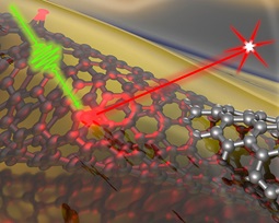
The researchers have provided an illustration of doped carbon nanotubes,

The deposition of a silicon dioxide layer (yellow layer) on a carbon nanotube (gray spheres) introduces solitary oxygen dopants (red spheres). A single photon (red and white star) is emitted when a dopant is excited by a laser pulse (green arrow). Image courtesy of the Center for Integrated Nanotechnologies

The deposition of a silicon dioxide layer (yellow layer) on a carbon nanotube (gray spheres) introduces solitary oxygen dopants (red spheres). A single photon (red and white star) is emitted when a dopant is excited by a laser pulse (green arrow). Image courtesy of the Center for Integrated Nanotechnologies

Here’s a link to and a citation for the paper, which was published a surprisingly long time ago,

Room-temperature single-photon generation from solitary dopants of carbon nanotubes by Xuedan Ma, Nicolai F. Hartmann, Jon K. S. Baldwin, Stephen K. Doorn, & Han Htoon.  Nature Nanotechnology 10, 671–675 (2015)  doi:10.1038/nnano.2015.136 Published online 13 July 2015

This paper is behind a paywall.

Carbon nanotubes transport protons faster than bulk water

An April 4, 2016 news item on Science Daily focuses on carbon nanotubes that measure eight-tenths of a nanometre and transport protons more quickly than bulk water by an order of magnitude,

For the first time, Lawrence Livermore National Laboratory (LLNL) researchers have shown that carbon nanotubes as small as eight-tenths of a nanometer in diameter can transport protons faster than bulk water, by an order of magnitude.

The research validates a 200-year old mechanism of proton transport.

A US Department of Energy Lawrence Livermore National Laboratory (LLNL) news release on EurekAlert, which originated the news item, provides more explanation,

The transport rates in these nanotube pores, which form one-dimensional water wires, also exceed those of biological channels and man-made proton conductors, making carbon nanotubes the fastest known proton conductor. …

Practical applications include proton exchange membranes, proton-based signaling in biological systems and the emerging field of proton bioelectronics (protonics).

“The cool thing about our results is that we found that when you squeeze water into the nanotube, protons move through that water even faster than through normal (bulk) water,” said Aleksandr Noy, an LLNL biophysicist and a lead author of the paper. (Bulk water is similar to what you would find in a cup of water that is much bigger than the size of a single water molecule).

The idea that protons travel fast in solutions by hopping along chains of hydrogen-bonded water molecules dates back 200 years to the work of Theodore von Grotthuss and still remains the foundation of the scientific understanding of proton transport. In the new research, LLNL researchers used carbon nanotube pores to line up water molecules into perfect one-dimensional chains and showed that they allow proton transport rates to approach the ultimate limits for the Grotthuss transport mechanism.

“The possibility to achieve fast proton transport by changing the degree of water confinement is exciting,” Noy said. “So far, the man-made proton conductors, such as polymer Nafion, use a different principle to enhance the proton transport. We have mimicked the way biological systems enhance the proton transport, took it to the extreme, and now our system realizes the ultimate limit of proton conductivity in a nanopore.”

Of all man-made materials, the narrow hydrophobic inner pores of carbon nanotubes (CNT) hold the most promise to deliver the level of confinement and weak interactions with water molecules that facilitate the formation of one-dimensional hydrogen-bonded water chains that enhance proton transport.

Earlier molecular dynamic simulations showed that water in 0.8 nm diameter carbon nanotubes would create such water wires and predicted that these channels would exhibit proton transport rates that would be much faster than those of bulk water. Ramya Tunuguntla, an LLNL postdoctoral researcher and the first author on the paper, said that despite significant efforts in carbon nanotube transport studies, these predictions proved to be hard to validate, mainly because of the difficulties in creating sub-1-nm diameter CNT pores.

However, the Lawrence Livermore team along with colleagues from the Lawrence Berkeley National Lab and UC Berkeley was able to create a simple and versatile experimental system for studying transport in ultra-narrow CNT pores. They used carbon nanotube porins (CNTPs), a technology they developed earlier at LLNL, which uses carbon nanotubes embedded in the lipid membrane to mimic biological ion channel functionality. The key breakthrough was the creation of nanotube porins with a diameter of less than 1 nm, which allowed researchers for the first time to achieve true one-dimensional water confinement.

Here’s a link to and a citation for the paper,

Ultrafast proton transport in sub-1-nm diameter carbon nanotube porins by Ramya H. Tunuguntla, Frances I. Allen, Kyunghoon Kim, Allison Belliveau, & Aleksandr Noy. Nature Nanotechnology (2016) doi:10.1038/nnano.2016.43 Published online 04 April 2016

This paper is behind a paywall.

Nature-inspired nanotubes from the Lawrence Berkeley National* Laboratory

A March 29, 2016 news item on Nanotechnology Now  announces a new technique for nature-inspired self-assembling polymer nanotubes,

When it comes to the various nanowidgets scientists are developing, nanotubes are especially intriguing. That’s because hollow tubes that have diameters of only a few billionths of a meter have the potential to be incredibly useful, from delivering cancer-fighting drugs inside cells to desalinating seawater.

But building nanostructures is difficult. And creating a large quantity of nanostructures with the same trait, such as millions of nanotubes with identical diameters, is even more difficult. This kind of precision manufacturing is needed to create the nanotechnologies of tomorrow.

Help could be on the way. As reported online the week of March 28 [2016] in the journal Proceedings of the National Academy of Sciences [PNAS], researchers at the U.S. Department of Energy’s Lawrence Berkeley National Laboratory (Berkeley Lab) have discovered a family of nature-inspired polymers that, when placed in water, spontaneously assemble into hollow crystalline nanotubes. What’s more, the nanotubes can be tuned to all have the same diameter of between five and ten nanometers, depending on the length of the polymer chain.

A March 28, 2016 Berkeley Lab news release (also on EurekAlert), which originated the news item, provides more detail,

The polymers have two chemically distinct blocks that are the same size and shape. The scientists learned these blocks act like molecular tiles that form rings, which stack together to form nanotubes up to 100 nanometers long, all with the same diameter.

“This points to a new way we can use synthetic polymers to create complex nanostructures in a very precise way,” says Ron Zuckermann, who directs the Biological Nanostructures Facility in Berkeley Lab’s Molecular Foundry, where much of this research was conducted.

Several other Berkeley Lab scientists contributed to this research, including Nitash Balsara of the Materials Sciences Division and Ken Downing of the Molecular Biophysics and Integrated Bioimaging Division.

“Creating uniform structures in high yield is a goal in nanotechnology,” adds Zuckermann. “For example, if you can control the diameter of nanotubes, and the chemical groups exposed in their interior, then you can control what goes through—which could lead to new filtration and desalination technologies, to name a few examples.”

The research is the latest in the effort to build nanostructures that approach the complexity and function of nature’s proteins, but are made of durable materials. In this work, the Berkeley Lab scientists studied a polymer that is a member of the peptoid family. Peptoids are rugged synthetic polymers that mimic peptides, which nature uses to form proteins. They can be tuned at the atomic scale to carry out specific functions.

For the past several years, the scientists have studied a particular type of peptoid, called a diblock copolypeptoid, because it binds with lithium ions and could be used as a battery electrolyte. Along the way, they serendipitously found the compounds form nanotubes in water. How exactly these nanotubes form has yet to be determined, but this latest research sheds light on their structure, and hints at a new design principle that could be used to build nanotubes and other complex nanostructures.

Diblock copolypeptoids are composed of two peptoid blocks, one that’s hydrophobic one that’s hydrophilic. The scientists discovered both blocks crystallize when they meet in water, and form rings consisting of two to three individual peptoids. The rings then form hollow nanotubes.

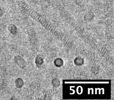
Cryo-electron microscopy imaging of 50 of the nanotubes showed the diameter of each tube is highly uniform along its length, as well as from tube to tube. This analysis also revealed a striped pattern across the width of the nanotubes, which indicates the rings stack together to form tubes, and rules out other packing arrangements. In addition, the peptoids are thought to arrange themselves in a brick-like pattern, with hydrophobic blocks lining up with other hydrophobic blocks, and the same for hydrophilic blocks.

“Images of the tubes captured by electron microscopy were essential for establishing the presence of this unusual structure,” says Balsara. “The formation of tubular structures with a hydrophobic core is common for synthetic polymers dispersed in water, so we were quite surprised to see the formation of hollow tubes without a hydrophobic core.”

X-ray scattering analyses conducted at beamline 7.3.3 of the Advanced Light Source revealed even more about the nanotubes’ structure. For example, it showed that one of the peptoid blocks, which is usually amorphous, is actually crystalline.

Remarkably, the nanotubes assemble themselves without the usual nano-construction aids, such as electrostatic interactions or hydrogen bond networks.

“You wouldn’t expect something as intricate as this could be created without these crutches,” says Zuckermann. “But it turns out the chemical interactions that hold the nanotubes together are very simple. What’s special here is that the two peptoid blocks are chemically distinct, yet almost exactly the same size, which allows the chains to pack together in a very regular way. These insights could help us design useful nanotubes and other structures that are rugged and tunable—and which have uniform structures.”

This cryo-electron microscopy image shows the self-assembling nanotubes have the same diameter. The circles are head-on views of nanotubes. The dark-striped features likely result from crystallized peptoid blocks. (Credit: Berkeley Lab)

This cryo-electron microscopy image shows the self-assembling nanotubes have the same diameter. The circles are head-on views of nanotubes. The dark-striped features likely result from crystallized peptoid blocks. (Credit: Berkeley Lab)

Here’s a link to and a citation for the paper,

Self-assembly of crystalline nanotubes from monodisperse amphiphilic diblock copolypeptoid tiles by Jing Sun, Xi Jiang, Reidar Lund, Kenneth H. Downing, Nitash P. Balsara, and Ronald N. Zuckermann. PNAS 2016 ; published ahead of print March 28, 2016, doi: 10.1073/pnas.1517169113

This paper is behind a paywall.

*’Lawrence Berkeley Laboratory’ changed to ‘Lawrence Berkeley National Laboratory’ on April 3, 2016.

US Nanotechnology Initiative for water sustainability

Wednesday, March 23, 2016 was World Water Day and to coincide with that event the US National Nanotechnology Initiative (NNI) in collaboration with several other agencies announced a new ‘signature initiative’. From a March 24, 2016 news item on Nanowerk (Note: A link has been removed),

As a part of the White House Water Summit held yesterday on World Water Day, the Federal agencies participating in the National Nanotechnology Initiative (NNI) announced the launch of a Nanotechnology Signature Initiative (NSI), Water Sustainability through Nanotechnology: Nanoscale Solutions for a Global-Scale Challenge.

A March 23, 2016 NNI news release provides more information about why this initiative is important,

Access to clean water remains one of the world’s most pressing needs. As today’s White House Office of Science and Technology blog post explains, “the small size and exceptional properties of engineered nanomaterials are particularly promising for addressing the key technical challenges related to water quality and quantity.”

“One cannot find an issue more critical to human life and global security than clean, plentiful, and reliable water sources,” said Dr. Michael Meador, Director of the National Nanotechnology Coordination Office (NNCO). “Through the NSI mechanism, NNI member agencies will have an even greater ability to make meaningful strides toward this initiative’s thrust areas: increasing water availability, improving the efficiency of water delivery and use, and enabling next-generation water monitoring systems.”

A March 23, 2016 US White House blog posting by Lloyd Whitman and Lisa Friedersdorf describes the efforts in more detail (Note: A link has been removed),

The small size and exceptional properties of engineered nanomaterials are particularly promising for addressing the pressing technical challenges related to water quality and quantity. For example, the increased surface area—a cubic centimeter of nanoparticles has a surface area larger than a football field—and reactivity of nanometer-scale particles can be exploited to create catalysts for water purification that do not require rare or precious metals. And composites incorporating nanomaterials such as carbon nanotubes might one day enable stronger, lighter, and more durable piping systems and components. Under this NSI, Federal agencies will coordinate and collaborate to more rapidly develop nanotechnology-enabled solutions in three main thrusts: [thrust 1] increasing water availability; [thrust 2] improving the efficiency of water delivery and use; and [thrust 3] enabling next-generation water monitoring systems.

A technical “white paper” released by the agencies this week highlights key technical challenges for each thrust, identifies key objectives to overcome those challenges, and notes areas of research and development where nanotechnology promises to provide the needed solutions. By shining a spotlight on these areas, the new NSI will increase Federal coordination and collaboration, including with public and private stakeholders, which is vital to making progress in these areas. The additional focus and associated collective efforts will advance stewardship of water resources to support the essential food, energy, security, and environment needs of all stakeholders.

We applaud the commitment of the Federal agencies who will participate in this effort—the Department of Commerce/National Institute of Standards and Technology, Department of Energy, Environmental Protection Agency, National Aeronautics and Space Administration, National Science Foundation, and U.S. Department of Agriculture/National Institute of Food and Agriculture. As made clear at this week’s White House Water Summit, the world’s water systems are under tremendous stress, and new and emerging technologies will play a critical role in ensuring a sustainable water future.

The white paper (12 pp.) is titled: Water Sustainability through Nanotechnology: Nanoscale Solutions for a Global-Scale Challenge and describes the thrusts in more detail.

A March 22, 2016 US White House fact sheet lays out more details including funding,

Click here to learn more about all of the commitments and announcements being made today. They include:

  • Nearly $4 billion in private capital committed to investment in a broad range of water-infrastructure projects nationwide. This includes $1.5 billion from Ultra Capital to finance decentralized and scalable water-management solutions, and $500 million from Sustainable Water to develop water reclamation and reuse systems.
  • More than $1 billion from the private sector over the next decade to conduct research and development into new technologies. This includes $500 million from GE to fuel innovation, expertise, and global capabilities in advanced water, wastewater, and reuse technologies.
  • A Presidential Memorandum and supporting Action Plan on building national capabilities for long-term drought resilience in the United States, including by setting drought resilience policy goals, directing specific drought resilience activities to be completed by the end of the year, and permanently establishing the National Drought Resilience Partnership as an interagency task force responsible for coordinating drought-resilience, response, and recovery efforts.
  • Nearly $35 million this year in Federal grants from the Environmental Protection Agency, the National Oceanic and Atmospheric Administration, the National Science Foundation, and the U.S. Department of Agriculture to support cutting-edge water science;
  • The release of a new National Water Model that will dramatically enhance the Nation’s river-forecasting capabilities by delivering forecasts for approximately 2.7 million locations, up from 4,000 locations today (a 700-fold increase in forecast density).

This seems promising and hopefully other countries will follow suit.

When an atom more or less makes a big difference

As scientists continue exploring the nanoscale, it seems that finding the number of atoms in your particle makes a difference is no longer so surprising. From a Jan. 28, 2016 news item on ScienceDaily,

Combining experimental investigations and theoretical simulations, researchers have explained why platinum nanoclusters of a specific size range facilitate the hydrogenation reaction used to produce ethane from ethylene. The research offers new insights into the role of cluster shapes in catalyzing reactions at the nanoscale, and could help materials scientists optimize nanocatalysts for a broad class of other reactions.

A Jan. 28, 2016 Georgia Institute of Technology (Georgia Tech) news release (*also on EurekAlert*), which originated the news item, expands on the theme,

At the macro-scale, the conversion of ethylene has long been considered among the reactions insensitive to the structure of the catalyst used. However, by examining reactions catalyzed by platinum clusters containing between 9 and 15 atoms, researchers in Germany and the United States found that at the nanoscale, that’s no longer true. The shape of nanoscale clusters, they found, can dramatically affect reaction efficiency.

While the study investigated only platinum nanoclusters and the ethylene reaction, the fundamental principles may apply to other catalysts and reactions, demonstrating how materials at the very smallest size scales can provide different properties than the same material in bulk quantities. …

“We have re-examined the validity of a very fundamental concept on a very fundamental reaction,” said Uzi Landman, a Regents’ Professor and F.E. Callaway Chair in the School of Physics at the Georgia Institute of Technology. “We found that in the ultra-small catalyst range, on the order of a nanometer in size, old concepts don’t hold. New types of reactivity can occur because of changes in one or two atoms of a cluster at the nanoscale.”

The widely-used conversion process actually involves two separate reactions: (1) dissociation of H2 molecules into single hydrogen atoms, and (2) their addition to the ethylene, which involves conversion of a double bond into a single bond. In addition to producing ethane, the reaction can also take an alternative route that leads to the production of ethylidyne, which poisons the catalyst and prevents further reaction.

The project began with Professor Ueli Heiz and researchers in his group at the Technical University of Munich experimentally examining reaction rates for clusters containing 9, 10, 11, 12 or 13 platinum atoms that had been placed atop a magnesium oxide substrate. The 9-atom nanoclusters failed to produce a significant reaction, while larger clusters catalyzed the ethylene hydrogenation reaction with increasingly better efficiency. The best reaction occurred with 13-atom clusters.

Bokwon Yoon, a research scientist in Georgia Tech’s Center for Computational Materials Science, and Landman, the center’s director, then used large-scale first-principles quantum mechanical simulations to understand how the size of the clusters – and their shape – affected the reactivity. Using their simulations, they discovered that the 9-atom cluster resembled a symmetrical “hut,” while the larger clusters had bulges that served to concentrate electrical charges from the substrate.

“That one atom changes the whole activity of the catalyst,” Landman said. “We found that the extra atom operates like a lightning rod. The distribution of the excess charge from the substrate helps facilitate the reaction. Platinum 9 has a compact shape that doesn’t facilitate the reaction, but adding just one atom changes everything.”

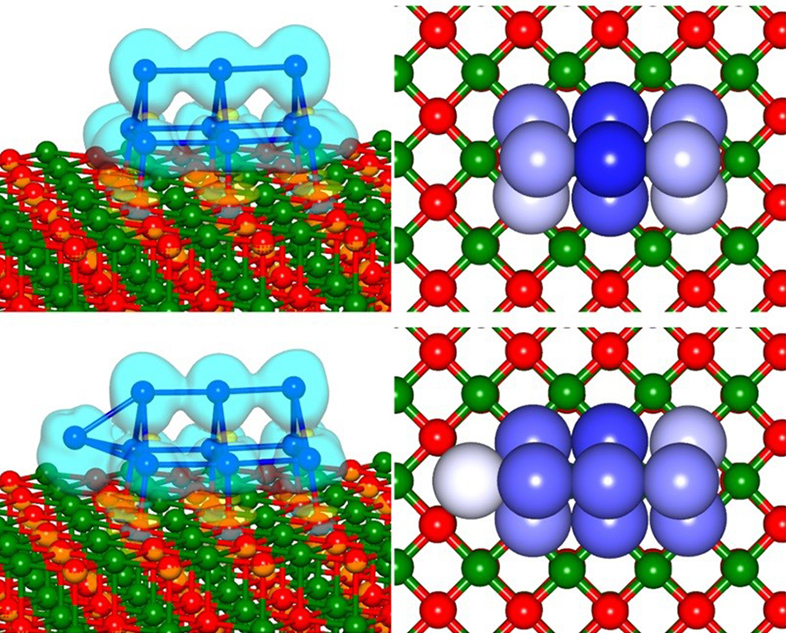
Here’s an illustration featuring the difference between a 9 atom cluster and a 10 atom cluster,

A single atom makes a difference in the catalytic properties of platinum nanoclusters. Shown are platinum 9 (top) and platinum 10 (bottom). (Credit: Uzi Landman, Georgia Tech)

A single atom makes a difference in the catalytic properties of platinum nanoclusters. Shown are platinum 9 (top) and platinum 10 (bottom). (Credit: Uzi Landman, Georgia Tech)

The news release explains why the larger clusters function as catalysts,

Nanoclusters with 13 atoms provided the maximum reactivity because the additional atoms shift the structure in a phenomena Landman calls “fluxionality.” This structural adjustment has also been noted in earlier work of these two research groups, in studies of clusters of gold [emphasis mine] which are used in other catalytic reactions.

“Dynamic fluxionality is the ability of the cluster to distort its structure to accommodate the reactants to actually enhance reactivity,” he explained. “Only very small aggregates of metal can show such behavior, which mimics a biochemical enzyme.”

The simulations showed that catalyst poisoning also varies with cluster size – and temperature. The 10-atom clusters can be poisoned at room temperature, while the 13-atom clusters are poisoned only at higher temperatures, helping to account for their improved reactivity.

“Small really is different,” said Landman. “Once you get into this size regime, the old rules of structure sensitivity and structure insensitivity must be assessed for their continued validity. It’s not a question anymore of surface-to-volume ratio because everything is on the surface in these very small clusters.”

While the project examined only one reaction and one type of catalyst, the principles governing nanoscale catalysis – and the importance of re-examining traditional expectations – likely apply to a broad range of reactions catalyzed by nanoclusters at the smallest size scale. Such nanocatalysts are becoming more attractive as a means of conserving supplies of costly platinum.

“It’s a much richer world at the nanoscale than at the macroscopic scale,” added Landman. “These are very important messages for materials scientists and chemists who wish to design catalysts for new purposes, because the capabilities can be very different.”

Along with the experimental surface characterization and reactivity measurements, the first-principles theoretical simulations provide a unique practical means for examining these structural and electronic issues because the clusters are too small to be seen with sufficient resolution using most electron microscopy techniques or traditional crystallography.

“We have looked at how the number of atoms dictates the geometrical structure of the cluster catalysts on the surface and how this geometrical structure is associated with electronic properties that bring about chemical bonding characteristics that enhance the reactions,” Landman added.

I highlighted the news release’s reference to gold nanoclusters as I have noted the number issue in two April 14, 2015 postings, neither of which featured Georgia Tech, Gold atoms: sometimes they’re a metal and sometimes they’re a molecule and Nature’s patterns reflected in gold nanoparticles.

Here’s a link to and a citation for the ‘platinum catalyst’ paper,

Structure sensitivity in the nonscalable regime explored via catalysed ethylene hydrogenation on supported platinum nanoclusters by Andrew S. Crampton, Marian D. Rötzer, Claron J. Ridge, Florian F. Schweinberger, Ueli Heiz, Bokwon Yoon, & Uzi Landman.  Nature Communications 7, Article number: 10389  doi:10.1038/ncomms10389 Published 28 January 2016

This paper is open access.

*’also on EurekAlert’ added Jan. 29, 2016.

Weaving at the nanoscale

A Jan. 21, 2016 news item on ScienceDaily announces a brand new technique,

For the first time, scientists have been able to weave a material at molecular level. The research is led by University of California Berkeley, in cooperation with Stockholm University. …

A Jan. 21, 2016 Stockholm University press release, which originated the news item, provides more information,

Weaving is a well-known way of making fabric, but has until now never been used at the molecular level. Scientists have now been able to weave organic threads into a three-dimensional material, using copper as a template. The new material is a COF, covalent organic framework, and is named COF-505. The copper ions can be removed and added without changing the underlying structure, and at the same time the elasticity can be reversibly changed.

– It almost looks like a molecular version of the Vikings chain-armour. The material is very flexible, says Peter Oleynikov, researcher at the Department of Materials and Environmental Chemistry at Stockholm University.

COF’s are like MOF’s porous three-dimensional crystals with a very large internal surface that can adsorb and store enormous quantities of molecules. A potential application is capture and storage of carbon dioxide, or using COF’s as a catalyst to make useful molecules from carbon dioxide.

Complex structure determined in Stockholm

The research is led by Professor Omar Yaghi at University of California Berkeley. At Stockholm University Professor Osamu Terasaki, PhD Student Yanhang Ma and Researcher Peter Oleynikov have contributed to determine the structure of COF-505 at atomic level from a nano-crystal, using electron crystallography methods.

– It is a difficult, complicated structure and it was very demanding to resolve. We’ve spent lot of time and efforts on the structure solution. Now we know exactly where the copper is and we can also replace the metal. This opens up many possibilities to make other materials, says Yanhang Ma, PhD Student at the Department of Materials and Environmental Chemistry at Stockholm University.

Another of the collaborating institutions, US Department of Energy Lawrence Berkeley National Laboratory issued a Jan. 21, 2016 news release on EurekAlert, providing a different perspective and some additional details,

There are many different ways to make nanomaterials but weaving, the oldest and most enduring method of making fabrics, has not been one of them – until now. An international collaboration led by scientists at the U.S. Department of Energy (DOE)’s Lawrence Berkeley National Laboratory (Berkeley Lab) and the University of California (UC) Berkeley, has woven the first three-dimensional covalent organic frameworks (COFs) from helical organic threads. The woven COFs display significant advantages in structural flexibility, resiliency and reversibility over previous COFs – materials that are highly prized for their potential to capture and store carbon dioxide then convert it into valuable chemical products.

“Weaving in chemistry has been long sought after and is unknown in biology,” Yaghi says [Omar Yaghi, chemist who holds joint appointments with Berkeley Lab’s Materials Sciences Division and UC Berkeley’s Chemistry Department and is the co-director of the Kavli Energy NanoScience Institute {Kavli-ENSI}]. “However, we have found a way of weaving organic threads that enables us to design and make complex two- and three-dimensional organic extended structures.”

COFs and their cousin materials, metal organic frameworks (MOFs), are porous three-dimensional crystals with extraordinarily large internal surface areas that can absorb and store enormous quantities of targeted molecules. Invented by Yaghi, COFs and MOFs consist of molecules (organics for COFs and metal-organics for MOFs) that are stitched into large and extended netlike frameworks whose structures are held together by strong chemical bonds. Such frameworks show great promise for, among other applications, carbon sequestration.

Through another technique developed by Yaghi, called “reticular chemistry,” these frameworks can also be embedded with catalysts to carry out desired functions: for example, reducing carbon dioxide into carbon monoxide, which serves as a primary building block for a wide range of chemical products including fuels, pharmaceuticals and plastics.

In this latest study, Yaghi and his collaborators used a copper(I) complex as a template for bringing threads of the organic compound “phenanthroline” into a woven pattern to produce an immine-based framework they dubbed COF-505. Through X-ray and electron diffraction characterizations, the researchers discovered that the copper(I) ions can be reversibly removed or restored to COF-505 without changing its woven structure. Demetalation of the COF resulted in a tenfold increase in its elasticity and remetalation restored the COF to its original stiffness.

“That our system can switch between two states of elasticity reversibly by a simple operation, the first such demonstration in an extended chemical structure, means that cycling between these states can be done repeatedly without degrading or altering the structure,” Yaghi says. “Based on these results, it is easy to imagine the creation of molecular cloths that combine unusual resiliency, strength, flexibility and chemical variability in one material.”

Yaghi says that MOFs can also be woven as can all structures based on netlike frameworks. In addition, these woven structures can also be made as nanoparticles or polymers, which means they can be fabricated into thin films and electronic devices.

“Our weaving technique allows long threads of covalently linked molecules to cross at regular intervals,” Yaghi says. “These crossings serve as points of registry, so that the threads have many degrees of freedom to move away from and back to such points without collapsing the overall structure, a boon to making materials with exceptional mechanical properties and dynamics.”

###

This research was primarily supported by BASF (Germany) and King Abdulaziz City for Science and Technology (KACST).

It’s unusual that neither Stockholm University not the Lawrence Berkeley National Laboratory list all of the institutions involved. To get a sense of this international collaboration’s size, I’m going to list them,

  • 1Department of Chemistry, University of California, Berkeley, Materials Sciences Division, Lawrence Berkeley National Laboratory, and Kavli Energy NanoSciences Institute, Berkeley, CA 94720, USA.
  • 2Department of Materials and Environmental Chemistry, Stockholm University, SE-10691 Stockholm, Sweden.
  • 3Department of New Architectures in Materials Chemistry, Materials Science Institute of Madrid, Consejo Superior de Investigaciones Científicas, Madrid 28049, Spain.
  • 4Nanomaterials Research Institute, National Institute of Advanced Industrial Science and Technology (AIST), Tsukuba 305-8565, Japan.
  • 5NSF Nanoscale Science and Engineering Center (NSEC), University of California at Berkeley, 3112 Etcheverry Hall, Berkeley, CA 94720, USA.
  • 6Advanced Light Source, Lawrence Berkeley National Laboratory, Berkeley, CA 94720, USA.
  • 7King Abdulaziz City of Science and Technology, Post Office Box 6086, Riyadh 11442, Saudi Arabia.
  • 8Material Sciences Division, Lawrence Berkeley National Laboratory, 1 Cyclotron Road, Berkeley, CA 94720, USA.
  • 9School of Physical Science and Technology, ShanghaiTech University, Shanghai 201210, China.

Given that some of the money came from a German company, I’m surprised not one German institution was involved.

Here’s a link to and citation for the paper,

Weaving of organic threads into a crystalline covalent organic framework by Yuzhong Liu, Yanhang Ma, Yingbo Zhao, Xixi Sun, Felipe Gándara, Hiroyasu Furukawa, Zheng Liu, Hanyu Zhu, Chenhui Zhu, Kazutomo Suenaga, Peter Oleynikov, Ahmad S. Alshammari, Xiang Zhang, Osamu Terasaki, Omar M. Yaghi. Science  22 Jan 2016: Vol. 351, Issue 6271, pp. 365-369 DOI: 10.1126/science.aad4011

This paper is behind a paywall.

A bioinspired approach to self-healing materials

Scientists have been working to develop self-healing materials for a while now and a Jan. 8, 2016 news item on Nanowerk chronicles a relatively recent attempt,

Inspired by healing wounds in skin, a new approach protects and heals surfaces using a fluid secretion process. In response to damage, dispersed liquid-storage droplets are controllably secreted. The stored liquid replenishes the surface and completes the repair of the polymer in seconds to hours …

The fluid secretion approach to repair the material has also been demonstrated in fibers and microbeads. This bioinspired approach could be extended to create highly desired adaptive, resilient materials with possible uses in heat transfer, humidity control, slippery surfaces, and fluid delivery.

A December ??, 2015 US Department of Energy (DOE) news release, which originated the news item, expands on the theme,

A polymer that secretes stored liquid in response to damage has been designed and created to function as a self-healing material. While human-made material systems can trigger the release of stored contents, the ability to continuously self-adjust and monitor liquid supply in these compartments is a challenge. In contrast, biological systems manage complex protection and healing functions by having individual components work in concert to initiate and self-regulate a coordinated response. Inspired by biological wound-healing, this new process, developed by researchers at Harvard University, involves trapping and dispersing liquid-storage droplets within a reversibly crosslinked polymer gel network topped with a thin liquid overlayer. This novel approach allows storage of the liquid, yet is reconfigurable to induce finely controlled secretion in response to polymer damage. When the gel was damaged by slicing, the ruptured droplets in the immediate vicinity of the damage released oil and the gel network was squeezed. This squeezing allowed oil to be pushed out from neighboring droplets and the polymer network linkages to unzip and rezip rapidly, allowing just enough oil to flow to the damaged region. Healing occurred at ambient temperature within seconds to hours as fluid was secreted into the crack, severed polymer ends diffused across the gap, and new network linkages were created. Droplet-embedded polymers repaired faster or at lower temperatures than polymers without oil droplets. Also, the repaired droplet-embedded materials were much stronger than the repaired networks that did not contain the droplets. This dynamic liquid exchange to repair the material has also been demonstrated in other forms, showing the potential to extend this bioinspired approach for fabricating highly desired adaptive, resilient materials to a wide range of polymeric structures.

Here’s a link to and a citation for the paper,

Dynamic polymer systems with self-regulated secretion for the control of surface properties and material healing by Jiaxi Cui, Daniel Daniel, Alison Grinthal, Kaixiang Lin, & Joanna Aizenberg. Nature Materials 14,  790–795 (2015) doi:10.1038/nmat4325 Published online 22 June 2015

I’m not sure what occasioned a late push to promote this particular piece of research but if you are interested, the paper is behind a paywall.

Canada has a nanotechnology industry? and an overview of the US situation

It’s always interesting to get some insight into how someone else sees the nanotechnology effort in Canada.

First, there have been two basic approaches internationally. Some countries have chosen to fund nanotechnology/nanoscience research through a national initiative/project/council/etc. Notably the US, the UK, China, and Russia, amongst others, have followed this model. For example, the US National Nanotechnology Initiative (NNI)  (a type of hub for research, communication, and commercialization efforts) has been awarded a portion of the US budget every year since 2000. The money is then disbursed through the National Science Foundation.

Canada and its nanotechnology industry efforts

By contrast, Canada has no such line item in its national budget. There is a National Institute of Nanotechnology (NINT) but it is one of many institutes that help make up Canada’s National Research Council. I’m not sure if this is still true but when it was first founded, NINT was funded in part by the federal government and in part by the province of Alberta where it is located (specifically, in Edmonton at the University of Alberta). They claim the organization has grown since its early days although it looks like it’s been shrinking. Perhaps some organizational shuffles? In any event, support for the Canadian nanotechnology efforts are more provincial than federal. Alberta (NINT and other agencies) and Québec (NanoQuébec, a provincially funded nano effort) are the standouts, with Ontario (nano Ontario, a self-organized not-for-profit group) following closely. The scene in Canada has always seemed fragmented in comparison to the countries that have nanotechnology ‘hubs’.

Patrick Johnson in a Dec. 22, 2015 article for Geopolitical Monitor offers a view which provides an overview of nanotechnology in the US and Canada,  adds to the perspective offered here, and, at times, challenges it (Note: A link has been added),

The term ‘nanotechnology’ entered into the public vernacular quite suddenly around the turn of the century, right around the same time that, when announcing the US National Nanotechnology Initiative (NNI) in 2001 [2000; see the American Association for the Advancement of Science webpage on Historical Trends in Federal R&D, scroll down to the National Nanotechnology Initiative and click on the Jpg or Excel links], President Bill Clinton declared that it would one day build materials stronger than steel, detect cancer at its inception, and store the vast records of the Library of Congress in a device the size of a sugar cube. The world of science fiction took matters even further. In his 2002 book Prey, Michael Creighton [Michael Crichton; see Wikipedia entry] wrote of a cloud of self-replicating nanorobots [also known as, nanobots or self-assemblers] that terrorize the good people of Nevada when a science experiment goes terribly wrong.

Back then the hype was palpable. Federal money was funneled to promising nanotech projects as not to fall behind in the race to master this new frontier of science. And industry analysts began to shoot for the moon in their projections. The National Science Foundation famously predicted that the nanotechnology industry would be worth $1 trillion by the year 2015.

Well here we are in 2015 and the nanotechnology market was worth around $26 billion in [sic] last year, and there hasn’t even been one case of a murderous swarm of nanomachines terrorizing the American heartland. [emphasis mine]

Is this a failure of vision? No. If anything it’s only a failure of timing.

The nanotechnology industry is still well on its way to accomplishing the goals set out at the founding of the NNI, goals which at the time sounded utterly quixotic, and this fact is increasingly being reflected in year-on-year growth numbers. In other words, nanotechnology is still a game-changer in global innovation, it’s just taking a little longer than first expected.

The Canadian Connection

Although the Canadian government is not among the world’s top spenders on nanotechnology research, the industry still represents a bright spot in the future of the Canadian economy. The public-private engine [emphasis mine] at the center of Canada’s nanotech industry, the National Institute for Nanotechnology (NINT), was founded in 2001 with the stated goal of “increasing the competitiveness of Canadian companies; creating technology solutions to meet the needs of society; expanding training programs for researchers and entrepreneurs; and enhancing Canada’s stature in the world of nanotechnology.” This ambitious mandate that NINT set out for itself was to be accomplished over the course of two broad stages: first a ‘seeding’ phase of attracting promising personnel and coordinating basic research, and the then a ‘harvesting’ phase of putting the resulting nanotechnologies to the service of Canadian industry.

Recent developments in Canadian nanotechnology [emphasis mine] show that we have already entered that second stage where the concept of nanotechnology transitions from hopeful hypothetical to real-world economic driver

I’d dearly like to know which recent developments indicate Canada’s industry has entered a serious commercialization phase. (It’s one of the shortcomings of our effort that communication is not well supported.) As well, I’d like to know more about the  “… public-private engine at the center of Canada’s nanotech industry …” as Johnson seems to be referring to the NINT, which is jointly funded (I believe) by the federal government and the province of Alberta. There is no mention of private funding on their National Research Council webpage but it does include the University of Alberta as a major supporter.

I am intrigued and I hope there is more information to come.

US and its nanotechnology industry efforts

Dr. Ambika Bumb has written a Dec. 23, 2015 article for Tech Crunch which reflects on her experience as a researcher and entrepreneur in the context of the US NNI effort and includes a plea for future NNI funding [Note: One link added and one link removed],

Indeed, I am fortunate to be the CEO of a nanomedicine technology developer that extends the hands of doctors and scientists to the cellular and molecular level.

The first seeds of interest in bringing effective nano-tools into the hands of doctors and patients were planted in my mind when I did undergrad research at Georgia Tech.  That initial interest led to me pursuing a PhD at Oxford University to develop a tri-modal nanoparticle for imaging a variety of diseases ranging from cancers to autoimmune disorders.

My graduate research only served to increase my curiosity so I then did a pair of post-doctoral fellowships at the National Cancer Institute and the National Heart Lung and Blood Institute.  When it seemed that I was a shoe-in for a life-long academic career, our technology garnered much attention and I found myself in the Bay Area founding the now award-winning Bikanta [bikanta.com].

Through the National Nanotechnology Initiative (NNI) and Nanotechnology Research and Development Act of 2003, our federal government has invested $20 billion in nanoresearch in the past 13 years.  The return on that investment has resulted in 628 agency‐to‐agency collaborations, hundreds of thousands of publications, and more than $1 trillion in revenue generated from nano‐enabled products. [emphasis mine]

Given that medical innovations take a minimum of 10 years before they translate into a clinical product, already realizing a 50X return is an astounding achievement.  Slowing down would be counter-intuitive from an academic and business perspective.

Yet, that is what is happening.  Federal funding peaked half a decade ago in 2010.  [emphasis mine] NNI investments went from $1.58B in 2010 to $1.170B in 2015 (in constant dollars), a 26% drop.  The number of nano-related papers published in the US were roughly 25 thousand in 2013, while the EU and China produced 33 and 35 thousand, respectively.

History has shown repeatedly how the United States has lost an early competitive advantage in developing high‐value technologies to international competition when commercialization infrastructure was not adequately supported.

Examples include semiconductors, advanced batteries for vehicles, and cement‐based construction materials, all of which were originally developed in the United States, but are now manufactured elsewhere.

It is now time for a second era – NNI 2.0.  A return to higher and sustained investment, the purpose of NNI 2.0 should be not just foundational research but also necessary support for rapid commercialization of nanotechnology. The translation of bench science into commercial reality requires the partnership of academic, industrial, federal, and philanthropic players.

I’m not sure why there’s a difference between Johnson’s ” … worth around $26 billion in [sic] last year …] and Bumb’s “… return on that investment has resulted … more than $1 trillion in revenue generated from nano‐enabled products.” I do know there is some controversy as to what should or should not be included when estimating the value of the ‘nanotechnology enterprise’, for example, products that are only possible due to nanotechnology as opposed to products that already existed, such as golf clubs, but are enhanced by nanotechnology.

Bumb goes on to provide a specific example from her own experience to support the plea,

When I moved from the renowned NIH [US National Institutes of Health] on the east coast to the west coast to start Bikanta, one of the highest priority concerns was how we were going to develop nanodiamond technology without access to high-end characterization instrumentation to analyze the quality of our material.  Purchasing all that equipment was not financially viable or even wise for a startup.

We were extremely lucky because our proposal was accepted by the Molecular Foundry, one of five DOE [US Department of Energy]-funded nanoscience user facilities.  While the Foundry primarily facilitates basic nanoscience projects from academic and national laboratory users, Fortune 500 companies and startups like ours also take advantage of its capabilities to answer fundamental questions and conduct proof of concept studies (~10%).

Disregarding the dynamic intellectual community for a minute, there is probably more than $150M worth of instrumentation at the Foundry.  An early startup would never be able to dream of raising a first round that large.

One of the factors of Bikanta’s success is that the Molecular Foundry enabled us to make tremendous strides in R&D in just months instead of years.  More user facilities, incubator centers, and funding for commercializing nanotech are greatly needed.

Final comments

I have to thank Dr. Bumb for pointing out that 2010 was the peak for NNI funding (see the American Association for the Advancement of Science webpage on Historical Trends in Federal R&D, scroll down to the National Nanotechnology Initiative and click on the Jpg or Excel links). I erroneously believed (although I don’t appear to have written up my belief; if you find any such statement, please let me know so I can correct it) that the 2015 US budget was the first time the NNI experienced a drop in funding.

While I found Johnson’s article interesting I wasn’t able to determine the source for his numbers and some of his material had errors that can be identified immediately, e.g., Michael Creighton instead of Michael Crichton.
US Los Alamos National Laboratory catches the D-Wave (buys a 1000+ Qubit quantum computer from D-Wave)

It can be euphoric experience making a major technical breakthrough (June 2015), selling to a new large customer (Nov. 2015) and impressing your important customers so they upgrade to the new system (Oct. 2015) within a few short months.* D-Wave Systems (a Vancouver-based quantum computer company) certainly has cause to experience it given the events of the last six weeks or so. Yesterday, in a Nov. 11, 2015, D-Wave news release, the company trumpeted its sale of a 1000+ Qubit system (Note: Links have been removed),

D-Wave Systems Inc., the world’s first quantum computing company, announced that Los Alamos National Laboratory will acquire and install the latest D-Wave quantum computer, the 1000+ qubit D-Wave 2X™ system. Los Alamos, a multidisciplinary research institution engaged in strategic science on behalf of national security, will lead a collaboration within the Department of Energy and with select university partners to explore the capabilities and applications of quantum annealing technology, consistent with the goals of the government-wide National Strategic Computing Initiative. The National Strategic Computing Initiative, created by executive order of President Obama in late July [2015], is intended “to maximize [the] benefits of high-performance computing (HPC) research, development, and deployment.”

“Los Alamos is a global leader in high performance computing and a pioneer in the application of new architectures to solve critical problems related to national security, energy, the environment, materials, health and earth science,” said Robert “Bo” Ewald, president of D-Wave U.S. “As we work jointly with scientists and engineers at Los Alamos we expect to be able to accelerate the pace of quantum software development to advance the state of algorithms, applications and software tools for quantum computing.”

A Nov. 11, 2015 news item on Nanotechnology Now is written from the company’s venture capitalist’s perspective,

Harris & Harris Group, Inc. (NASDAQ:TINY), an investor in transformative companies enabled by disruptive science, notes that its portfolio company, D-Wave Systems, Inc., announced that Los Alamos National Laboratory will acquire and install the latest D-Wave quantum computer, the 1000+ qubit D-Wave 2X™ system.

The news about the Los Alamos sale comes only weeks after D-Wave announced renewed agreements with Google, NASA (US National Aeronautics and Space Administration), and the Universities Space Research Association (USRA) in the aftermath of a technical breakthrough. See my Oct. 5, 2015 posting for more details about the agreements, the type of quantum computer D-Wave sells, and news of interesting and related research in Australia. Cracking the 512 qubit barrier also occasioned a posting here (June 26, 2015) where I described the breakthrough, the company, and included excerpts from an Economist article which mentioned D-Wave in its review of research in the field of quantum computing.

Congratulations to D-Wave!

*’It can be euphoric selling to your first large and/or important customers and D-Wave Systems (a Vancouver-based quantum computer company) certainly has cause to experience it. ‘ changed to more accurately express my thoughts to ‘It can be euphoric experience making a major technical breakthrough (June 2015), selling to a new large customer (Nov. 2015) and impressing your important customers so they upgrade to the new system (Oct. 2015) within a few short months.’ on Nov. 12, 2015 at 1025 hours PST.

Nature-inspired but not really, a new design rule for nanostructures

It’s fascinating to observe the news release writer’s attempt to package this research as biomimetic when the new design rule is not found in nature. An Oct. 7, 2015 news item on ScienceDaily provides an introduction to the work from the Lawrence Berkeley National Laboratory,

Scientists aspire to build nanostructures that mimic the complexity and function of nature’s proteins. These microscopic widgets could be customized into incredibly sensitive chemical detectors or long-lasting catalysts. But as with any craft that requires extreme precision, researchers must first learn how to finesse the materials they’ll use to build these structures. A new discovery is a big step in this direction. The scientists discovered a design rule that enables a recently created material to exist.

An Oct. 7, 2015 Lawrence Berekeley National Laboratory (Berkeley Lab) news release (also on EurekAlert), which originated the news item, features more detail about the research and the writer’s gyrations,

The scientists discovered a design rule that enables a recently created material to exist. The material is a peptoid nanosheet. It’s a flat structure only two molecules thick, and it’s composed of peptoids, which are synthetic polymers closely related to protein-forming peptides.

The design rule controls the way in which polymers adjoin to form the backbones that run the length of nanosheets. Surprisingly, these molecules link together in a counter-rotating pattern not seen in nature. [emphasis mine] This pattern allows the backbones to remain linear and untwisted, a trait that makes peptoid nanosheets larger and flatter than any biological structure.

The Berkeley Lab scientists say this never-before-seen design rule could be used to piece together complex nanosheet structures and other peptoid assemblies such as nanotubes and crystalline solids.

What’s more, they discovered it by combining computer simulations with x-ray scattering and imaging methods to determine, for the first time, the atomic-resolution structure of peptoid nanosheets.

“This research suggests new ways to design biomimetic structures, [emphasis mine]” says Steve Whitelam, a co-corresponding author of the Nature paper. “We can begin thinking about using design principles other than those nature offers.”

The news release goes on to note the previous work which this newest research builds on and provides yet more detail about the latest and greatest,

Peptoid nanosheets were discovered by Zuckermann’s group five years ago. They found that under the right conditions, peptoids self assemble into two-dimensional assemblies that can grow hundreds of microns across. This “molecular paper” has become a hot prospect as a protein-mimicking platform for molecular design.

To learn more about this potential building material, the scientists set out to learn its atom-resolution structure. This involved feedback between experiment and theory. Microscopy and scattering data gathered at the Molecular Foundry and the Advanced Light Source, also a DOE Office of Science user facility located at Berkeley Lab, were compared with molecular dynamics simulations conducted at NERSC.

The research revealed several new things about peptoid nanosheets. Their molecular makeup varies throughout their structure, they can be formed only from peptoids of a certain minimum length, they contain water pockets, and they are potentially porous when it comes to water and ions.

These insights are intriguing on their own, but when the scientists examined the structure of the nanosheets’ backbone, they were surprised to see a design rule not found in the field of protein structural biology.

Here’s the difference: In nature, proteins are composed of beta sheets and alpha helices. These fundamental building blocks are themselves composed of backbones, and the polymers that make up these backbones are all joined together using the same rule. Each adjacent polymer rotates incrementally in the same direction, so that a twist runs along the backbone.

This rule doesn’t apply to peptoid nanosheets. Along their backbones, adjacent monomer units rotate in opposite directions. These counter-rotations cancel each other out, resulting in a linear and untwisted backbone. This enables backbones to be tiled in two dimensions and extended into large sheets that are flatter than anything nature can produce.

“It was a big surprise to find the design rule that makes peptoid nanosheets possible has eluded the field of biology until now,” says Mannige [Ranjan Mannige, a postdoctoral researcher at the Molecular Foundry]. “This rule could perhaps be used to build many more unrealized structures.”

Adds Zuckermann [Peptoid nanosheets were discovered by Zuckermann’s group five years ago. They found that under the right conditions, peptoids self assemble into two-dimensional assemblies that can grow hundreds of microns across. This “molecular paper” has become a hot prospect as a protein-mimicking platform for molecular design.

To learn more about this potential building material, the scientists set out to learn its atom-resolution structure. This involved feedback between experiment and theory. Microscopy and scattering data gathered at the Molecular Foundry and the Advanced Light Source, also a DOE Office of Science user facility located at Berkeley Lab, were compared with molecular dynamics simulations conducted at NERSC.

The research revealed several new things about peptoid nanosheets. Their molecular makeup varies throughout their structure, they can be formed only from peptoids of a certain minimum length, they contain water pockets, and they are potentially porous when it comes to water and ions.

These insights are intriguing on their own, but when the scientists examined the structure of the nanosheets’ backbone, they were surprised to see a design rule not found in the field of protein structural biology.

Here’s the difference: In nature, proteins are composed of beta sheets and alpha helices. These fundamental building blocks are themselves composed of backbones, and the polymers that make up these backbones are all joined together using the same rule. Each adjacent polymer rotates incrementally in the same direction, so that a twist runs along the backbone.

This rule doesn’t apply to peptoid nanosheets. Along their backbones, adjacent monomer units rotate in opposite directions. These counter-rotations cancel each other out, resulting in a linear and untwisted backbone. This enables backbones to be tiled in two dimensions and extended into large sheets that are flatter than anything nature can produce.

“It was a big surprise to find the design rule that makes peptoid nanosheets possible has eluded the field of biology until now,” says Mannige. “This rule could perhaps be used to build many more unrealized structures.”

Adds Zuckermann, [Ron Zuckermann directs the Molecular Foundry’s Biological Nanostructures Facility.] “We also expect there are other design principles waiting to be discovered, which could lead to even more biomimetic nanostructures.”

They might have been better off describing the work as “bioinspired” but it is a tricky thing to describe and there doesn’t seem to be an easy way out of describing this discovery which is based on observations from nature but follows no rule found in nature.

Here’s a link to and a citation for the paper,

Peptoid nanosheets exhibit a new secondary-structure motif by Ranjan V. Mannige, Thomas K. Haxton, Caroline Proulx, Ellen J. Robertson, Alessia Battigelli, Glenn L. Butterfoss, Ronald N. Zuckermann, & Stephen Whitelam. Nature (2015) doi:10.1038/nature15363 Published online 07 October 2015

This paper is behind a paywall.