Tag Archives: IEEE (Institute of Electrical and Electronics Engineers)

Mott memristor

Mott memristors (mentioned in my Aug. 24, 2017 posting about neuristors and brainlike computing) gets more fulsome treatment in an Oct. 9, 2017 posting by Samuel K. Moore on the Nanoclast blog (found on the IEEE [Institute of Electrical and Electronics Engineers] website) Note: 1: Links have been removed; Note 2 : I quite like Moore’s writing style but he’s not for the impatient reader,

When you’re really harried, you probably feel like your head is brimful of chaos. You’re pretty close. Neuroscientists say your brain operates in a regime termed the “edge of chaos,” and it’s actually a good thing. It’s a state that allows for fast, efficient analog computation of the kind that can solve problems that grow vastly more difficult as they become bigger in size.

The trouble is, if you’re trying to replicate that kind of chaotic computation with electronics, you need an element that both acts chaotically—how and when you want it to—and could scale up to form a big system.

“No one had been able to show chaotic dynamics in a single scalable electronic device,” says Suhas Kumar, a researcher at Hewlett Packard Labs, in Palo Alto, Calif. Until now, that is.

He, John Paul Strachan, and R. Stanley Williams recently reported in the journal Nature that a particular configuration of a certain type of memristor contains that seed of controlled chaos. What’s more, when they simulated wiring these up into a type of circuit called a Hopfield neural network, the circuit was capable of solving a ridiculously difficult problem—1,000 instances of the traveling salesman problem—at a rate of 10 trillion operations per second per watt.

(It’s not an apples-to-apples comparison, but the world’s most powerful supercomputer as of June 2017 managed 93,015 trillion floating point operations per second but consumed 15 megawatts doing it. So about 6 billion operations per second per watt.)

The device in question is called a Mott memristor. Memristors generally are devices that hold a memory, in the form of resistance, of the current that has flowed through them. The most familiar type is called resistive RAM (or ReRAM or RRAM, depending on who’s asking). Mott memristors have an added ability in that they can also reflect a temperature-driven change in resistance.

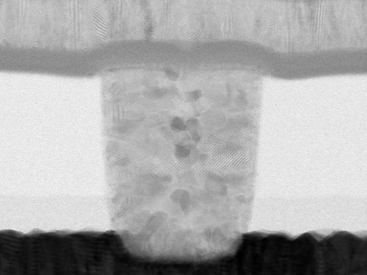
The HP Labs team made their memristor from an 8-nanometer-thick layer of niobium dioxide (NbO2) sandwiched between two layers of titanium nitride. The bottom titanium nitride layer was in the form of a 70-nanometer wide pillar. “We showed that this type of memristor can generate chaotic and nonchaotic signals,” says Williams, who invented the memristor based on theory by Leon Chua.

(The traveling salesman problem is one of these. In it, the salesman must find the shortest route that lets him visit all of his customers’ cities, without going through any of them twice. It’s a difficult problem because it becomes exponentially more difficult to solve with each city you add.)

Here’s what the niobium dioxide-based Mott memristor looks like,

Photo: Suhas Kumar/Hewlett Packard Labs
A micrograph shows the construction of a Mott memristor composed of an 8-nanometer-thick layer of niobium dioxide between two layers of titanium nitride.

Here’s a link to and a citation for the paper,

Chaotic dynamics in nanoscale NbO2 Mott memristors for analogue computing by Suhas Kumar, John Paul Strachan & R. Stanley Williams. Nature 548, 318–321 (17 August 2017) doi:10.1038/nature23307 Published online: 09 August 2017

This paper is behind a paywall.

Yarns that harvest and generate energy

The researchers involved in this work are confident enough about their prospects that they will be  patenting their research into yarns. From an August 25, 2017 news item on Nanowerk,

An international research team led by scientists at The University of Texas at Dallas and Hanyang University in South Korea has developed high-tech yarns that generate electricity when they are stretched or twisted.

In a study published in the Aug. 25 [2017] issue of the journal Science (“Harvesting electrical energy from carbon nanotube yarn twist”), researchers describe “twistron” yarns and their possible applications, such as harvesting energy from the motion of ocean waves or from temperature fluctuations. When sewn into a shirt, these yarns served as a self-powered breathing monitor.

“The easiest way to think of twistron harvesters is, you have a piece of yarn, you stretch it, and out comes electricity,” said Dr. Carter Haines, associate research professor in the Alan G. MacDiarmid NanoTech Institute at UT Dallas and co-lead author of the article. The article also includes researchers from South Korea, Virginia Tech, Wright-Patterson Air Force Base and China.

An August 25, 2017 University of Texas at Dallas news release, which originated the news item, expands on the theme,

Yarns Based on Nanotechnology

The yarns are constructed from carbon nanotubes, which are hollow cylinders of carbon 10,000 times smaller in diameter than a human hair. The researchers first twist-spun the nanotubes into high-strength, lightweight yarns. To make the yarns highly elastic, they introduced so much twist that the yarns coiled like an over-twisted rubber band.

In order to generate electricity, the yarns must be either submerged in or coated with an ionically conducting material, or electrolyte, which can be as simple as a mixture of ordinary table salt and water.

“Fundamentally, these yarns are supercapacitors,” said Dr. Na Li, a research scientist at the NanoTech Institute and co-lead author of the study. “In a normal capacitor, you use energy — like from a battery — to add charges to the capacitor. But in our case, when you insert the carbon nanotube yarn into an electrolyte bath, the yarns are charged by the electrolyte itself. No external battery, or voltage, is needed.”

When a harvester yarn is twisted or stretched, the volume of the carbon nanotube yarn decreases, bringing the electric charges on the yarn closer together and increasing their energy, Haines said. This increases the voltage associated with the charge stored in the yarn, enabling the harvesting of electricity.

Stretching the coiled twistron yarns 30 times a second generated 250 watts per kilogram of peak electrical power when normalized to the harvester’s weight, said Dr. Ray Baughman, director of the NanoTech Institute and a corresponding author of the study.

“Although numerous alternative harvesters have been investigated for many decades, no other reported harvester provides such high electrical power or energy output per cycle as ours for stretching rates between a few cycles per second and 600 cycles per second.”

Lab Tests Show Potential Applications

In the lab, the researchers showed that a twistron yarn weighing less than a housefly could power a small LED, which lit up each time the yarn was stretched.

To show that twistrons can harvest waste thermal energy from the environment, Li connected a twistron yarn to a polymer artificial muscle that contracts and expands when heated and cooled. The twistron harvester converted the mechanical energy generated by the polymer muscle to electrical energy.

“There is a lot of interest in using waste energy to power the Internet of Things, such as arrays of distributed sensors,” Li said. “Twistron technology might be exploited for such applications where changing batteries is impractical.”

The researchers also sewed twistron harvesters into a shirt. Normal breathing stretched the yarn and generated an electrical signal, demonstrating its potential as a self-powered respiration sensor.

“Electronic textiles are of major commercial interest, but how are you going to power them?” Baughman said. “Harvesting electrical energy from human motion is one strategy for eliminating the need for batteries. Our yarns produced over a hundred times higher electrical power per weight when stretched compared to other weavable fibers reported in the literature.”

Electricity from Ocean Waves

“In the lab we showed that our energy harvesters worked using a solution of table salt as the electrolyte,” said Baughman, who holds the Robert A. Welch Distinguished Chair in Chemistry in the School of Natural Sciences and Mathematics. “But we wanted to show that they would also work in ocean water, which is chemically more complex.”

In a proof-of-concept demonstration, co-lead author Dr. Shi Hyeong Kim, a postdoctoral researcher at the NanoTech Institute, waded into the frigid surf off the east coast of South Korea to deploy a coiled twistron in the sea. He attached a 10 centimeter-long yarn, weighing only 1 milligram (about the weight of a mosquito), between a balloon and a sinker that rested on the seabed.

Every time an ocean wave arrived, the balloon would rise, stretching the yarn up to 25 percent, thereby generating measured electricity.

Even though the investigators used very small amounts of twistron yarn in the current study, they have shown that harvester performance is scalable, both by increasing twistron diameter and by operating many yarns in parallel.

“If our twistron harvesters could be made less expensively, they might ultimately be able to harvest the enormous amount of energy available from ocean waves,” Baughman said. “However, at present these harvesters are most suitable for powering sensors and sensor communications. Based on demonstrated average power output, just 31 milligrams of carbon nanotube yarn harvester could provide the electrical energy needed to transmit a 2-kilobyte packet of data over a 100-meter radius every 10 seconds for the Internet of Things.”

Researchers from the UT Dallas Erik Jonsson School of Engineering and Computer Science and Lintec of America’s Nano-Science & Technology Center also participated in the study.

The investigators have filed a patent on the technology.

In the U.S., the research was funded by the Air Force, the Air Force Office of Scientific Research, NASA, the Office of Naval Research and the Robert A. Welch Foundation. In Korea, the research was supported by the Korea-U.S. Air Force Cooperation Program and the Creative Research Initiative Center for Self-powered Actuation of the National Research Foundation and the Ministry of Science.

Here’s a link to and a citation for the paper,

Harvesting electrical energy from carbon nanotube yarn twist by Shi Hyeong Kim, Carter S. Haines, Na Li, Keon Jung Kim, Tae Jin Mun, Changsoon Choi, Jiangtao Di, Young Jun Oh, Juan Pablo Oviedo, Julia Bykova, Shaoli Fang, Nan Jiang, Zunfeng Liu, Run Wang, Prashant Kumar, Rui Qiao, Shashank Priya, Kyeongjae Cho, Moon Kim, Matthew Steven Lucas, Lawrence F. Drummy, Benji Maruyama, Dong Youn Lee, Xavier Lepró, Enlai Gao, Dawood Albarq, Raquel Ovalle-Robles, Seon Jeong Kim, Ray H. Baughman. Science 25 Aug 2017: Vol. 357, Issue 6353, pp. 773-778 DOI: 10.1126/science.aam8771

This paper is behind a paywall.

Dexter Johnson in an Aug. 25, 2017 posting on his Nanoclast blog (on the IEEE [Institute of Electrical and Electronics Engineers] website) delves further into the research,

“Basically what’s happening is when we stretch the yarn, we’re getting a change in capacitance of the yarn. It’s that change that allows us to get energy out,” explains Carter Haines, associate research professor at UT Dallas and co-lead author of the paper describing the research, in an interview with IEEE Spectrum.

This makes it similar in many ways to other types of energy harvesters. For instance, in other research, it has been demonstrated—with sheets of rubber with coated electrodes on both sides—that you can increase the capacitance of a material when you stretch it and it becomes thinner. As a result, if you have charge on that capacitor, you can change the voltage associated with that charge.

“We’re more or less exploiting the same effect but what we’re doing differently is we’re using an electric chemical cell to do this,” says Haines. “So we’re not changing double layer capacitance in normal parallel plate capacitors. But we’re actually changing the electric chemical capacitance on the surface of a super capacitor yarn.”

While there are other capacitance-based energy harvesters, those other devices require extremely high voltages to work because they’re using parallel plate capacitors, according to Haines.

Dexter asks good questions and his post is very informative.
IBM and a 5 nanometre chip

If this continues, they’re going to have change the scale from nano to pico. IBM has announced work on a 5 nanometre (5nm) chip in a June 5, 2017 news item on Nanotechnology Now,

IBM (NYSE: IBM), its Research Alliance partners GLOBALFOUNDRIES and Samsung, and equipment suppliers have developed an industry-first process to build silicon nanosheet transistors that will enable 5 nanometer (nm) chips. The details of the process will be presented at the 2017 Symposia on VLSI Technology and Circuits conference in Kyoto, Japan. In less than two years since developing a 7nm test node chip with 20 billion transistors, scientists have paved the way for 30 billion switches on a fingernail-sized chip.

A June 5, 2017 IBM news release, which originated the news item, spells out some of the details about IBM’s latest breakthrough,

The resulting increase in performance will help accelerate cognitive computing [emphasis mine], the Internet of Things (IoT), and other data-intensive applications delivered in the cloud. The power savings could also mean that the batteries in smartphones and other mobile products could last two to three times longer than today’s devices, before needing to be charged.

Scientists working as part of the IBM-led Research Alliance at the SUNY Polytechnic Institute Colleges of Nanoscale Science and Engineering’s NanoTech Complex in Albany, NY achieved the breakthrough by using stacks of silicon nanosheets as the device structure of the transistor, instead of the standard FinFET architecture, which is the blueprint for the semiconductor industry up through 7nm node technology.

“For business and society to meet the demands of cognitive and cloud computing in the coming years, advancement in semiconductor technology is essential,” said Arvind Krishna, senior vice president, Hybrid Cloud, and director, IBM Research. “That’s why IBM aggressively pursues new and different architectures and materials that push the limits of this industry, and brings them to market in technologies like mainframes and our cognitive systems.”

The silicon nanosheet transistor demonstration, as detailed in the Research Alliance paper Stacked Nanosheet Gate-All-Around Transistor to Enable Scaling Beyond FinFET, and published by VLSI, proves that 5nm chips are possible, more powerful, and not too far off in the future.

Compared to the leading edge 10nm technology available in the market, a nanosheet-based 5nm technology can deliver 40 percent performance enhancement at fixed power, or 75 percent power savings at matched performance. This improvement enables a significant boost to meeting the future demands of artificial intelligence (AI) systems, virtual reality and mobile devices.

Building a New Switch

“This announcement is the latest example of the world-class research that continues to emerge from our groundbreaking public-private partnership in New York,” said Gary Patton, CTO and Head of Worldwide R&D at GLOBALFOUNDRIES. “As we make progress toward commercializing 7nm in 2018 at our Fab 8 manufacturing facility, we are actively pursuing next-generation technologies at 5nm and beyond to maintain technology leadership and enable our customers to produce a smaller, faster, and more cost efficient generation of semiconductors.”

IBM Research has explored nanosheet semiconductor technology for more than 10 years. This work is the first in the industry to demonstrate the feasibility to design and fabricate stacked nanosheet devices with electrical properties superior to FinFET architecture.

This same Extreme Ultraviolet (EUV) lithography approach used to produce the 7nm test node and its 20 billion transistors was applied to the nanosheet transistor architecture. Using EUV lithography, the width of the nanosheets can be adjusted continuously, all within a single manufacturing process or chip design. This adjustability permits the fine-tuning of performance and power for specific circuits – something not possible with today’s FinFET transistor architecture production, which is limited by its current-carrying fin height. Therefore, while FinFET chips can scale to 5nm, simply reducing the amount of space between fins does not provide increased current flow for additional performance.

“Today’s announcement continues the public-private model collaboration with IBM that is energizing SUNY-Polytechnic’s, Albany’s, and New York State’s leadership and innovation in developing next generation technologies,” said Dr. Bahgat Sammakia, Interim President, SUNY Polytechnic Institute. “We believe that enabling the first 5nm transistor is a significant milestone for the entire semiconductor industry as we continue to push beyond the limitations of our current capabilities. SUNY Poly’s partnership with IBM and Empire State Development is a perfect example of how Industry, Government and Academia can successfully collaborate and have a broad and positive impact on society.”

Part of IBM’s $3 billion, five-year investment in chip R&D (announced in 2014), the proof of nanosheet architecture scaling to a 5nm node continues IBM’s legacy of historic contributions to silicon and semiconductor innovation. They include the invention or first implementation of the single cell DRAM, the Dennard Scaling Laws, chemically amplified photoresists, copper interconnect wiring, Silicon on Insulator, strained engineering, multi core microprocessors, immersion lithography, high speed SiGe, High-k gate dielectrics, embedded DRAM, 3D chip stacking and Air gap insulators.

I last wrote about IBM and computer chips in a July 15, 2015 posting regarding their 7nm chip. You may want to scroll down approximately 55% of the way where I note research from MIT (Massachusetts Institute of Technology) about metal nanoparticles with unexpected properties possibly having an impact on nanoelectronics.

Getting back to IBM, they have produced a slick video about their 5nm chip breakthrough,

Meanwhile, Katherine Bourzac provides technical detail in a June 5, 2017 posting on the Nanoclast blog (on the IEEE [Institute of Electrical and Electronics Engineers] website), Note: A link has been removed,

Researchers at IBM believe the future of the transistor is in stacked nanosheets. …

Today’s state-of-the-art transistor is the finFET, named for the fin-like ridges of current-carrying silicon that project from the chip’s surface. The silicon fins are surrounded on their three exposed sides by a structure called the gate. The gate switches the flow of current on, and prevents electrons from leaking out when the transistor is off. This design is expected to last from this year’s bleeding-edge process technology, the “10-nanometer” node, through the next node, 7 nanometers. But any smaller, and these transistors will become difficult to switch off: electrons will leak out, even with the three-sided gates.

So the semiconductor industry has been working on alternatives for the upcoming 5 nanometer node. One popular idea is to use lateral silicon nanowires that are completely surrounded by the gate, preventing electron leaks and saving power. This design is called “gate all around.” IBM’s new design is a variation on this. In their test chips, each transistor is made up of three stacked horizontal sheets of silicon, each only a few nanometers thick and completely surrounded by a gate.

Why a sheet instead of a wire? Huiming Bu, director of silicon integration and devices at IBM, says nanosheets can bring back one of the benefits of pre-finFET, planar designs. Designers used to be able to vary the width of a transistor to prioritize fast operations or energy efficiency. Varying the amount of silicon in a finFET transistor is not practicable because it would mean making some fins taller and other shorter. Fins must all be the same height due to manufacturing constraints, says Bu.

IBM’s nanosheets can range from 8 to 50 nanometers in width. “Wider gives you better performance but takes more power, smaller width relaxes performance but reduces power use,” says Bu. This will allow circuit designers to pick and choose what they need, whether they are making a power efficient mobile chip processor or designing a bank of SRAM memory. “We are bringing flexibility back to the designers,” he says.

The test chips have 30 billion transistors. …

It was a struggle trying to edit Bourzac’s posting with its good detail and clear writing. I encourage you to read it (June 5, 2017 posting) in its entirety.

As for where this drive downwards to the ‘ever smaller’ is going, there’s Dexter’s Johnson’s June 29, 2017 posting about another IBM team’s research on his Nanoclast blog on the IEEE website (Note: Links have been removed),

There have been increasing signs coming from the research community that carbon nanotubes are beginning to step up to the challenge of offering a real alternative to silicon-based complementary metal-oxide semiconductor (CMOS) transistors.

Now, researchers at IBM Thomas J. Watson Research Center have advanced carbon nanotube-based transistors another step toward meeting the demands of the International Technology Roadmap for Semiconductors (ITRS) for the next decade. The IBM researchers have fabricated a p-channel transistor based on carbon nanotubes that takes up less than half the space of leading silicon technologies while operating at a lower voltage.

In research described in the journal Science, the IBM scientists used a carbon nanotube p-channel to reduce the transistor footprint; their transistor contains all components to 40 square nanometers [emphasis mine], an ITRS roadmap benchmark for ten years out.

One of the keys to being able to reduce the transistor to such a small size is the use of the carbon nanotube as the channel in place of silicon. The nanotube is only 1 nanometer thick. Such thinness offers a significant advantage in electrostatics, so that it’s possible to reduce the device gate length to 10 nanometers without seeing the device performance adversely affected by short-channel effects. An additional benefit of the nanotubes is that the electrons travel much faster, which contributes to a higher level of device performance.

Happy reading!

Solar-powered graphene skin for more feeling in your prosthetics

A March 23, 2017 news item on Nanowerk highlights research that could put feeling into a prosthetic limb,

A new way of harnessing the sun’s rays to power ‘synthetic skin’ could help to create advanced prosthetic limbs capable of returning the sense of touch to amputees.

Engineers from the University of Glasgow, who have previously developed an ‘electronic skin’ covering for prosthetic hands made from graphene, have found a way to use some of graphene’s remarkable physical properties to use energy from the sun to power the skin.

Graphene is a highly flexible form of graphite which, despite being just a single atom thick, is stronger than steel, electrically conductive, and transparent. It is graphene’s optical transparency, which allows around 98% of the light which strikes its surface to pass directly through it, which makes it ideal for gathering energy from the sun to generate power.

A March 23, 2017 University of Glasgow press release, which originated the news item, details more about the research,

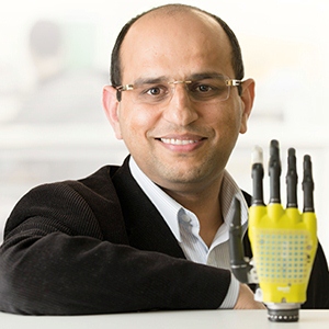
Ravinder Dahiya

Dr Ravinder Dahiya

A new research paper, published today in the journal Advanced Functional Materials, describes how Dr Dahiya and colleagues from his Bendable Electronics and Sensing Technologies (BEST) group have integrated power-generating photovoltaic cells into their electronic skin for the first time.

Dr Dahiya, from the University of Glasgow’s School of Engineering, said: “Human skin is an incredibly complex system capable of detecting pressure, temperature and texture through an array of neural sensors which carry signals from the skin to the brain.

“My colleagues and I have already made significant steps in creating prosthetic prototypes which integrate synthetic skin and are capable of making very sensitive pressure measurements. Those measurements mean the prosthetic hand is capable of performing challenging tasks like properly gripping soft materials, which other prosthetics can struggle with. We are also using innovative 3D printing strategies to build more affordable sensitive prosthetic limbs, including the formation of a very active student club called ‘Helping Hands’.

“Skin capable of touch sensitivity also opens the possibility of creating robots capable of making better decisions about human safety. A robot working on a construction line, for example, is much less likely to accidentally injure a human if it can feel that a person has unexpectedly entered their area of movement and stop before an injury can occur.”

The new skin requires just 20 nanowatts of power per square centimetre, which is easily met even by the poorest-quality photovoltaic cells currently available on the market. And although currently energy generated by the skin’s photovoltaic cells cannot be stored, the team are already looking into ways to divert unused energy into batteries, allowing the energy to be used as and when it is required.

Dr Dahiya added: “The other next step for us is to further develop the power-generation technology which underpins this research and use it to power the motors which drive the prosthetic hand itself. This could allow the creation of an entirely energy-autonomous prosthetic limb.

“We’ve already made some encouraging progress in this direction and we’re looking forward to presenting those results soon. We are also exploring the possibility of building on these exciting results to develop wearable systems for affordable healthcare. In this direction, recently we also got small funds from Scottish Funding Council.”

For more information about this advance and others in the field of prosthetics you may want to check out Megan Scudellari’s March 30, 2017 article for the IEEE’s (Institute of Electrical and Electronics Engineers) Spectrum (Note: Links have been removed),

Cochlear implants can restore hearing to individuals with some types of hearing loss. Retinal implants are now on the market to restore sight to the blind. But there are no commercially available prosthetics that restore a sense of touch to those who have lost a limb.

Several products are in development, including this haptic system at Case Western Reserve University, which would enable upper-limb prosthetic users to, say, pluck a grape off a stem or pull a potato chip out of a bag. It sounds simple, but such tasks are virtually impossible without a sense of touch and pressure.

Now, a team at the University of Glasgow that previously developed a flexible ‘electronic skin’ capable of making sensitive pressure measurements, has figured out how to power their skin with sunlight. …

Here’s a link to and a citation for the paper,

Energy-Autonomous, Flexible, and Transparent Tactile Skin by Carlos García Núñez, William Taube Navaraj, Emre O. Polat and Ravinder Dahiya. Advanced Functional Materials DOI: 10.1002/adfm.201606287 Version of Record online: 22 MAR 2017

© 2017 WILEY-VCH Verlag GmbH & Co. KGaA, Weinheim

This paper is behind a paywall.

R.I.P. Mildred Dresselhaus, Queen of Carbon

I’ve been hearing about Mildred Dresselhaus, professor emerita (retired professor) at the Massachusetts Institute of Technology (MIT), just about as long as I’ve been researching and writing about nanotechnology (about 10 years total* including the work for my master’s project with the almost eight years on this blog).

She died on Monday, Feb. 20, 2017 at the age of 86 having broken through barriers for those of her gender, barriers for her subject area, and barriers for her age.

Mark Anderson in his Feb. 22, 2017 obituary for the IEEE (Institute of Electrical and Electronics Engineers) Spectrum website provides a brief overview of her extraordinary life and accomplishments,

Called the “Queen of Carbon Science,” Dresselhaus pioneered the study of carbon nanostructures at a time when studying physical and material properties of commonplace atoms like carbon was out of favor. Her visionary perspectives on the sixth atom in the periodic table—including exploring individual layers of carbon atoms (precursors to graphene), developing carbon fibers stronger than steel, and revealing new carbon structures that were ultimately developed into buckyballs and nanotubes—invigorated the field.

“Millie Dresselhaus began life as the child of poor Polish immigrants in the Bronx; by the end, she was Institute Professor Emerita, the highest distinction awarded by the MIT faculty. A physicist, materials scientist, and electrical engineer, she was known as the ‘Queen of Carbon’ because her work paved the way for much of today’s carbon-based nanotechnology,” MIT president Rafael Reif said in a prepared statement.

Friends and colleagues describe Dresselhaus as a gifted instructor as well as a tireless and inspired researcher. And her boundless generosity toward colleagues, students, and girls and women pursuing careers in science is legendary.

In 1963, Dresselhaus began her own career studying carbon by publishing a paper on graphite in the IBM Journal for Research and Development, a foundational work in the history of nanotechnology. To this day, her studies of the electronic structure of this material serve as a reference point for explorations of the electronic structure of fullerenes and carbon nanotubes. Coauthor, with her husband Gene Dresselhaus, of a leading book on carbon fibers, she began studying the laser vaporation of carbon and the “carbon clusters” that resulted. Researchers who followed her lead discovered a 60-carbon structure that was soon identified as the icosahedral “soccer ball” molecular configuration known as buckminsterfullerene, or buckyball. In 1991, Dresselhaus further suggested that fullerene could be elongated as a tube, and she outlined these imagined objects’ symmetries. Not long after, researchers announced the discovery of carbon nanotubes.

When she began her nearly half-century career at MIT, as a visiting professor, women consisted of just 4 percent of the undergraduate student population.  So Dresselhaus began working toward the improvement of living conditions for women students at the university. Through her leadership, MIT adopted an equal and joint admission process for women and men. (Previously, MIT had propounded the self-fulfilling prophecy of harboring more stringent requirements for women based on less dormitory space and perceived poorer performance.) And so promoting women in STEM—before it was ever called STEM—became one of her passions. Serving as president of the American Physical Society, she spearheaded and launched initiatives like the Committee on the Status of Women in Physics and the society’s more informal committees of visiting women physicists on campuses around the United States, which have increased the female faculty and student populations on the campuses they visit.

If you have the time, please read Anderson’s piece in its entirety.

One fact that has impressed me greatly is that Dresselhaus kept working into her eighties. I featured a paper she published in an April 27, 2012 posting at the age of 82 and she was described in the MIT write up at the time as a professor, not a professor emerita. I later featured Dresselhaus in a May 31, 2012 posting when she was awarded the Kavli Prize for Nanoscience.

It seems she worked almost to the end. Recently, GE (General Electric) posted a video “What If Scientists Were Celebrities?” starring Mildred Dresselhaus,

H/t Mark Anderson’s obituary Feb. 22, 2017 piece. The video was posted on Feb. 8, 2017.

Goodbye to the Queen of Carbon!

*The word ‘total’ added on March 14, 2022.