Monthly Archives: January 2023

Efficient hydrogen evolution reaction with graphene-based NiSe2 nanocrystalline array

Should this work make its way from the laboratory to the market it could prove helpful in the drive to move away from fossil fuels, from a July 15, 2022 news item on Nanowerk,

In the face of low electrolytic water splitting catalytic activity, the development of efficiency and stable electrolytic catalyst for hydrogen evolution reaction is critical necessary. Moreover, the rather high price with insufficient supply of noble mental namely platinum and palladium has become the obstacle of their large-scale applications.

A research group of Lixu Lei from Southeast University [China] and Fajun Li from Suzhou University just reported a novel graphene based NiSe2 [nickel diselenide] nanocrystalline array prepared through a two-step microwave and subsequent selenization treatment. They found their unique structural advantages —— the ultrafine uniform dispersion of NiSe2 nanocrystallines in the reduced graphite oxide as substrate has an additional synergistic effect on promoting the conductivity and stability.

A July 15, 2022 Higher Education Press news release on EurekAlert, which originated the news item, provides more detail about the work,

Nickel selenide electrocatalysts for hydrogen evolution reaction with high efficiency and low-cost, has favorable potential future application prospect. Nevertheless, the high overpotential and poor stability limited their practical applications. Carbon materials including graphene, carbon nanotubes etc. possess extraordinary thermal stability and electric conductivity, can be ideal protective skeleton structures of electrocatalysts. By combining the NiSe2 nanoparticles with graphene sheet in an in-situ growth manner assisted with microwave irradiation, the electrocatalytic performance of hydrogen evolution reaction was optimized remarkably in this work.

The electrocatalytic activity for hydrogen evolution reaction of the composite proven can reach up to 158 mV overpotential at 10 mA/cm2 and has an extremely stable performance in the 100 h H2 production test. These results provide a useful idea for the development of newly high efficiency electrocatalyst for hydrogen evolution reaction.

About Higher Education Press

Founded in May 1954, Higher Education Press Limited Company (HEP), affiliated with the Ministry of Education, is one of the earliest institutions committed to educational publishing after the establishment of P. R. China in 1949. After striving for six decades, HEP has developed into a major comprehensive publisher, with products in various forms and at different levels. Both for import and export, HEP has been striving to fill in the gap of domestic and foreign markets and meet the demand of global customers by collaborating with more than 200 partners throughout the world and selling products and services in 32 languages globally. Now, HEP ranks among China’s top publishers in terms of copyright export volume and the world’s top 50 largest publishing enterprises in terms of comprehensive strength.

The Frontiers Journals series published by HEP includes 28 English academic journals, covering the largest academic fields in China at present. Among the series, 13 have been indexed by SCI, 6 by EI, 2 by MEDLINE, 1 by A&HCI. HEP’s academic monographs have won about 300 different kinds of publishing funds and awards both at home and abroad.

About Frontiers in Energy

Frontiers in Energy, a peer-reviewed international journal launched in January 2007, presents a unique platform for reporting the most advanced research and strategic thinking on energy technology. The Journal publishes review and mini-review articles, original research articles, perspective, news & highlights, viewpoints, comments, etc. by individual researchers and research groups. The journal is strictly peer-reviewed and accepts only original submissions in English. The scope of the Journal covers (but not limited to): energy conversion and utilization; renewable energy; energy storage; hydrogen and fuel cells; carbon capture, utilization and storage; advanced nuclear technology; smart grids and microgrids; power and energy systems; power cells and electric vehicles; building energy conservation, energy and environment; energy economy and policy, etc. Interdisciplinary papers are encouraged.

Here’s a link to and a citation for the paper,

In situ growth of NiSe2 nanocrystalline array on graphene for efficient hydrogen evolution reaction by Shuai Ji, Changgan Lai, Huan Zhou, Helin Wang, Ling Ma, Cong Wang, Keying Zhang, Fajun Li & Lixu Lei. Frontiers in Energy (2022) DOI: https://doi.org/10.1007/s11708-022-0827-7 Published 10 June 2022

This paper is behind a paywall.

What is CRISPRnano?

To answer the question, CRISPRnano is a computational webserver for identifying gene-edited cells. (For those unfamiliar with CRISPR, it stands for clustered regularly interspaced short palindromic repeats’ a form of gene editing,)

The webserver was announced in a July 15, 2022 news item on Nanowerk but first, there’s an explanation of why this server is needed,

Diseases of genetic cause can be investigated by inducing the respective mutations in cell lines that are then used to model human diseases. The overall aim is to elucidate underlying mechanisms, interactions with environmental factors and ideally to find curative strategies.

A crucial step in generating genetically modified cell models is to verify the inserted mutation. Therefore, the genetic information carrier of the cells is decoded (sequencing) and compared to the reference set of genetic information in healthy individuals (genotyping).

To support scientists with the comparison, different workflows and software are available, but many of them require expensive high-tier sequencers or manual curation efforts.

A July 15, 2022 IUF – Leibniz-Institut für umweltmedizinische Forschung (Leibniz Research Institute for Environmental Medicine) press release, which originated the news item, includes details about the server,

To address this issue, a team of scientists from the Genome Engineering and Model Development lab at the IUF – Leibniz Research Institute for Environmental Medicine in Düsseldorf, led by Dr. Andrea Rossi, developed a robust, versatile, and easy-to-use computational webserver named CRISPRnano (https://www.crisprnano.de/) that enables the analysis of noisy reads generated by affordable and portable sequencers including Oxford Nanopore Technologies (ONT) devices. CRISPRnano allows fast and accurate identification, quantification, and visualization of genetically modified cell lines, it is compatible with Next Generation Sequencing (NGS) and ONT sequencing reads, and it can be used without an internet connection. The according study was published in the renowned scientific journal Nucleic Acids Research.

Here’s a link to and a citation for the related study,

Identification of genome edited cells using CRISPRnano by Thach Nguyen, Haribaskar Ramachandran, Soraia Martins, Jean Krutmann, Andrea Rossi. Nucleic Acids Research, Volume 50, Issue W1, 5 July 2022, Pages W199–W203, DOI: https://doi.org/10.1093/nar/gkac440 Published: 30 May 2022

This paper appears to be open access.

Reconfiguring a LEGO-like AI chip with light

MIT engineers have created a reconfigurable AI chip that comprises alternating layers of sensing and processing elements that can communicate with each other. Credit: Figure courtesy of the researchers and edited by MIT News

This image certainly challenges any ideas I have about what Lego looks like. It seems they see things differently at the Massachusetts Institute of Technology (MIT). From a June 13, 2022 MIT news release (also on EurekAlert),

Imagine a more sustainable future, where cellphones, smartwatches, and other wearable devices don’t have to be shelved or discarded for a newer model. Instead, they could be upgraded with the latest sensors and processors that would snap onto a device’s internal chip — like LEGO bricks incorporated into an existing build. Such reconfigurable chipware could keep devices up to date while reducing our electronic waste. 

Now MIT engineers have taken a step toward that modular vision with a LEGO-like design for a stackable, reconfigurable artificial intelligence chip.

The design comprises alternating layers of sensing and processing elements, along with light-emitting diodes (LED) that allow for the chip’s layers to communicate optically. Other modular chip designs employ conventional wiring to relay signals between layers. Such intricate connections are difficult if not impossible to sever and rewire, making such stackable designs not reconfigurable.

The MIT design uses light, rather than physical wires, to transmit information through the chip. The chip can therefore be reconfigured, with layers that can be swapped out or stacked on, for instance to add new sensors or updated processors.

“You can add as many computing layers and sensors as you want, such as for light, pressure, and even smell,” says MIT postdoc Jihoon Kang. “We call this a LEGO-like reconfigurable AI chip because it has unlimited expandability depending on the combination of layers.”

The researchers are eager to apply the design to edge computing devices — self-sufficient sensors and other electronics that work independently from any central or distributed resources such as supercomputers or cloud-based computing.

“As we enter the era of the internet of things based on sensor networks, demand for multifunctioning edge-computing devices will expand dramatically,” says Jeehwan Kim, associate professor of mechanical engineering at MIT. “Our proposed hardware architecture will provide high versatility of edge computing in the future.”

The team’s results are published today in Nature Electronics. In addition to Kim and Kang, MIT authors include co-first authors Chanyeol Choi, Hyunseok Kim, and Min-Kyu Song, and contributing authors Hanwool Yeon, Celesta Chang, Jun Min Suh, Jiho Shin, Kuangye Lu, Bo-In Park, Yeongin Kim, Han Eol Lee, Doyoon Lee, Subeen Pang, Sang-Hoon Bae, Hun S. Kum, and Peng Lin, along with collaborators from Harvard University, Tsinghua University, Zhejiang University, and elsewhere.

Lighting the way

The team’s design is currently configured to carry out basic image-recognition tasks. It does so via a layering of image sensors, LEDs, and processors made from artificial synapses — arrays of memory resistors, or “memristors,” that the team previously developed, which together function as a physical neural network, or “brain-on-a-chip.” Each array can be trained to process and classify signals directly on a chip, without the need for external software or an Internet connection.

In their new chip design, the researchers paired image sensors with artificial synapse arrays, each of which they trained to recognize certain letters — in this case, M, I, and T. While a conventional approach would be to relay a sensor’s signals to a processor via physical wires, the team instead fabricated an optical system between each sensor and artificial synapse array to enable communication between the layers, without requiring a physical connection. 

“Other chips are physically wired through metal, which makes them hard to rewire and redesign, so you’d need to make a new chip if you wanted to add any new function,” says MIT postdoc Hyunseok Kim. “We replaced that physical wire connection with an optical communication system, which gives us the freedom to stack and add chips the way we want.”

The team’s optical communication system consists of paired photodetectors and LEDs, each patterned with tiny pixels. Photodetectors constitute an image sensor for receiving data, and LEDs to transmit data to the next layer. As a signal (for instance an image of a letter) reaches the image sensor, the image’s light pattern encodes a certain configuration of LED pixels, which in turn stimulates another layer of photodetectors, along with an artificial synapse array, which classifies the signal based on the pattern and strength of the incoming LED light.

Stacking up

The team fabricated a single chip, with a computing core measuring about 4 square millimeters, or about the size of a piece of confetti. The chip is stacked with three image recognition “blocks,” each comprising an image sensor, optical communication layer, and artificial synapse array for classifying one of three letters, M, I, or T. They then shone a pixellated image of random letters onto the chip and measured the electrical current that each neural network array produced in response. (The larger the current, the larger the chance that the image is indeed the letter that the particular array is trained to recognize.)

The team found that the chip correctly classified clear images of each letter, but it was less able to distinguish between blurry images, for instance between I and T. However, the researchers were able to quickly swap out the chip’s processing layer for a better “denoising” processor, and found the chip then accurately identified the images.

“We showed stackability, replaceability, and the ability to insert a new function into the chip,” notes MIT postdoc Min-Kyu Song.

The researchers plan to add more sensing and processing capabilities to the chip, and they envision the applications to be boundless.

“We can add layers to a cellphone’s camera so it could recognize more complex images, or makes these into healthcare monitors that can be embedded in wearable electronic skin,” offers Choi, who along with Kim previously developed a “smart” skin for monitoring vital signs.

Another idea, he adds, is for modular chips, built into electronics, that consumers can choose to build up with the latest sensor and processor “bricks.”

“We can make a general chip platform, and each layer could be sold separately like a video game,” Jeehwan Kim says. “We could make different types of neural networks, like for image or voice recognition, and let the customer choose what they want, and add to an existing chip like a LEGO.”

This research was supported, in part, by the Ministry of Trade, Industry, and Energy (MOTIE) from South Korea; the Korea Institute of Science and Technology (KIST); and the Samsung Global Research Outreach Program.

Here’s a link to and a citation for the paper,

Reconfigurable heterogeneous integration using stackable chips with embedded artificial intelligence by Chanyeol Choi, Hyunseok Kim, Ji-Hoon Kang, Min-Kyu Song, Hanwool Yeon, Celesta S. Chang, Jun Min Suh, Jiho Shin, Kuangye Lu, Bo-In Park, Yeongin Kim, Han Eol Lee, Doyoon Lee, Jaeyong Lee, Ikbeom Jang, Subeen Pang, Kanghyun Ryu, Sang-Hoon Bae, Yifan Nie, Hyun S. Kum, Min-Chul Park, Suyoun Lee, Hyung-Jun Kim, Huaqiang Wu, Peng Lin & Jeehwan Kim. Nature Electronics volume 5, pages 386–393 (2022) 05 May 2022 Issue Date: June 2022 Published: 13 June 2022 DOI: https://doi.org/10.1038/s41928-022-00778-y

This paper is behind a paywall.

Speaking in Color, an AI-powered paint tool

This June 16, 2022 article by Jeff Beer for Fast Company took me in an unexpected direction but first, there’s this from Beer’s story,

If an architect wanted to create a building that matched the color of a New York City summer sunset, they’d have to pore over potentially hundreds of color cards designed for industry to get anything close, and still it’d be a tall order to find that exact match. But a new AI-powered, voice-controlled tool from Sherwin-Williams aims to change that.

The paint brand recently launched Speaking in Color, a tool that allows users to tell it about certain places, objects, or shades in order to arrive at that perfect color. You start with a broad description like, say, “New York City summer sunset,” and then fine tune from there once it responds with photos and other options with more in-depth preferences like “darker red,” “make it moodier,” or “add a sliver of sun,” until it’s done.

Developed with agency Wunderman Thompson, it’s a React web app that uses natural language to find your preferred color using both third-party and proprietary code. The tool’s custom algorithm allows you to tweak colors in a way that translates statements like “make it dimmer,” “add warmth,” or “more like the 1980s” into mathematical adjustments.

It seems to me Wunderman Thompson needs to rethink its Sherwin Williams Speaking in Color promotional video (it’s embedded with Beer’s June 16, 2022 article or you can find it here; scroll down about 50% of the way). You’ll note, the color prompts are not spoken; they’re in text, e.g., ‘crystal-clear Caribbean ocean’. So much for ‘speaking in color’ but the article aroused my curiosity which is how I found this May 19, 2017 article by Annalee Newitz for Ars Technica highlighting another color/AI project (Note: A link has been removed),

At some point, we’ve all wondered about the incredibly strange names for paint colors. Research scientist and neural network goofball Janelle Shane took the wondering a step further. Shane decided to train a neural network to generate new paint colors, complete with appropriate names. The results are possibly the greatest work of artificial intelligence I’ve seen to date.

Writes Shane on her Tumblr, “For this experiment, I gave the neural network a list of about 7,700 Sherwin-Williams paint colors along with their RGB values. (RGB = red, green, and blue color values.) Could the neural network learn to invent new paint colors and give them attractive names?”

Shane told Ars that she chose a neural network algorithm called char-rnn, which predicts the next character in a sequence. So basically the algorithm was working on two tasks: coming up with sequences of letters to form color names, and coming up with sequences of numbers that map to an RGB value. As she checked in on the algorithm’s progress, she found that it was able to create colors long before it could actually name them reliably.

The longer it processed the dataset, the closer the algorithm got to making legit color names, though they were still mostly surreal: “Soreer Gray” is a kind of greenish color, and “Sane Green” is a purplish blue. When Shane cranked up “creativity” on the algorithm’s output, it gave her a violet color called “Dondarf” and a Kelly green called “Bylfgoam Glosd.” After churning through several more iterations of this process, Shane was able to get the algorithm to recognize some basic colors like red and gray, “though not reliably,” because she also gets a sky blue called “Gray Pubic” and a dark green called “Stoomy Brown.”

Brown has since written a book about artificial intelligence (You Look Like a Thing and I Love You; How Artificial Intelligence Works and Why It’s Making the World a Weirder Place [2019]) and continues her investigations of AI. You can find her website and blog here and her Wikipedia entry here.

Photonic synapses with low power consumption (and a few observations)

This work on brainlike (neuromorphic) computing was announced in a June 30, 2022 Compuscript Ltd news release on EurekAlert,

Photonic synapses with low power consumption and high sensitivity are expected to integrate sensing-memory-preprocessing capabilities

A new publication from Opto-Electronic Advances; DOI 10.29026/oea.2022.210069 discusses how photonic synapses with low power consumption and high sensitivity are expected to integrate sensing-memory-preprocessing capabilities.

Neuromorphic photonics/electronics is the future of ultralow energy intelligent computing and artificial intelligence (AI). In recent years, inspired by the human brain, artificial neuromorphic devices have attracted extensive attention, especially in simulating visual perception and memory storage. Because of its advantages of high bandwidth, high interference immunity, ultrafast signal transmission and lower energy consumption, neuromorphic photonic devices are expected to realize real-time response to input data. In addition, photonic synapses can realize non-contact writing strategy, which contributes to the development of wireless communication. The use of low-dimensional materials provides an opportunity to develop complex brain-like systems and low-power memory logic computers. For example, large-scale, uniform and reproducible transition metal dichalcogenides (TMDs) show great potential for miniaturization and low-power biomimetic device applications due to their excellent charge-trapping properties and compatibility with traditional CMOS processes. The von Neumann architecture with discrete memory and processor leads to high power consumption and low efficiency of traditional computing. Therefore, the sensor-memory fusion or sensor-memory- processor integration neuromorphic architecture system can meet the increasingly developing demands of big data and AI for low power consumption and high performance devices. Artificial synaptic devices are the most important components of neuromorphic systems. The performance evaluation of synaptic devices will help to further apply them to more complex artificial neural networks (ANN).

Chemical vapor deposition (CVD)-grown TMDs inevitably introduce defects or impurities, showed a persistent photoconductivity (PPC) effect. TMDs photonic synapses integrating synaptic properties and optical detection capabilities show great advantages in neuromorphic systems for low-power visual information perception and processing as well as brain memory.

The research Group of Optical Detection and Sensing (GODS) have reported a three-terminal photonic synapse based on the large-area, uniform multilayer MoS2 films. The reported device realized ultrashort optical pulse detection within 5 μs and ultralow power consumption about 40 aJ, which means its performance is much better than the current reported properties of photonic synapses. Moreover, it is several orders of magnitude lower than the corresponding parameters of biological synapses, indicating that the reported photonic synapse can be further used for more complex ANN. The photoconductivity of MoS2 channel grown by CVD is regulated by photostimulation signal, which enables the device to simulate short-term synaptic plasticity (STP), long-term synaptic plasticity (LTP), paired-pulse facilitation (PPF) and other synaptic properties. Therefore, the reported photonic synapse can simulate human visual perception, and the detection wavelength can be extended to near infrared light. As the most important system of human learning, visual perception system can receive 80% of learning information from the outside. With the continuous development of AI, there is an urgent need for low-power and high sensitivity visual perception system that can effectively receive external information. In addition, with the assistant of gate voltage, this photonic synapse can simulate the classical Pavlovian conditioning and the regulation of different emotions on memory ability. For example, positive emotions enhance memory ability and negative emotions weaken memory ability. Furthermore, a significant contrast in the strength of STP and LTP based on the reported photonic synapse suggests that it can preprocess the input light signal. These results indicate that the photo-stimulation and backgate control can effectively regulate the conductivity of MoS2 channel layer by adjusting carrier trapping/detrapping processes. Moreover, the photonic synapse presented in this paper is expected to integrate sensing-memory-preprocessing capabilities, which can be used for real-time image detection and in-situ storage, and also provides the possibility to break the von Neumann bottleneck. 

Here’s a link to and a citation for the paper,

Photonic synapses with ultralow energy consumption for artificial visual perception and brain storage by Caihong Li, Wen Du, Yixuan Huang, Jihua Zou, Lingzhi Luo, Song Sun, Alexander O. Govorov, Jiang Wu, Hongxing Xu, Zhiming Wang. Opto-Electron Adv Vol 5, No 9 210069 (2022). doi: 10.29026/oea.2022.210069

This paper is open access.

Observations

I don’t have much to say about the research itself other than, I believe this is the first time I’ve seen a news release about neuromorphic computing research from China.

it’s China that most interests me, especially these bits from the June 30, 2022 Compuscript Ltd news release on EurekAlert,

Group of Optical Detection and Sensing (GODS) [emphasis mine] was established in 2019. It is a research group focusing on compound semiconductors, lasers, photodetectors, and optical sensors. GODS has established a well-equipped laboratory with research facilities such as Molecular Beam Epitaxy system, IR detector test system, etc. GODS is leading several research projects funded by NSFC and National Key R&D Programmes. GODS have published more than 100 research articles in Nature Electronics, Light: Science and Applications, Advanced Materials and other international well-known high-level journals with the total citations beyond 8000.

Jiang Wu obtained his Ph.D. from the University of Arkansas Fayetteville in 2011. After his Ph.D., he joined UESTC as associate professor and later professor. He joined University College London [UCL] as a research associate in 2012 and then lecturer in the Department of Electronic and Electrical Engineering at UCL from 2015 to 2018. He is now a professor at UESTC [University of Electronic Science and Technology of China] [emphases mine]. His research interests include optoelectronic applications of semiconductor heterostructures. He is a Fellow of the Higher Education Academy and Senior Member of IEEE.

Opto-Electronic Advances (OEA) is a high-impact, open access, peer reviewed monthly SCI journal with an impact factor of 9.682 (Journals Citation Reports for IF 2020). Since its launch in March 2018, OEA has been indexed in SCI, EI, DOAJ, Scopus, CA and ICI databases over the time and expanded its Editorial Board to 36 members from 17 countries and regions (average h-index 49). [emphases mine]

The journal is published by The Institute of Optics and Electronics, Chinese Academy of Sciences, aiming at providing a platform for researchers, academicians, professionals, practitioners, and students to impart and share knowledge in the form of high quality empirical and theoretical research papers covering the topics of optics, photonics and optoelectronics.

The research group’s awkward name was almost certainly developed with the rather grandiose acronym, GODS, in mind. I don’t think you could get away with doing this in an English-speaking country as your colleagues would mock you mercilessly.

It’s Jiang Wu’s academic and work history that’s of most interest as it might provide insight into China’s Young Thousand Talents program. A January 5, 2023 American Association for the Advancement of Science (AAAS) news release describes the program,

In a systematic evaluation of China’s Young Thousand Talents (YTT) program, which was established in 2010, researchers find that China has been successful in recruiting and nurturing high-caliber Chinese scientists who received training abroad. Many of these individuals outperform overseas peers in publications and access to funding, the study shows, largely due to access to larger research teams and better research funding in China. Not only do the findings demonstrate the program’s relative success, but they also hold policy implications for the increasing number of governments pursuing means to tap expatriates for domestic knowledge production and talent development. China is a top sender of international students to United States and European Union science and engineering programs. The YTT program was created to recruit and nurture the productivity of high-caliber, early-career, expatriate scientists who return to China after receiving Ph.Ds. abroad. Although there has been a great deal of international attention on the YTT, some associated with the launch of the U.S.’s controversial China Initiative and federal investigations into academic researchers with ties to China, there has been little evidence-based research on the success, impact, and policy implications of the program itself. Dongbo Shi and colleagues evaluated the YTT program’s first 4 cohorts of scholars and compared their research productivity to that of their peers that remained overseas. Shi et al. found that China’s YTT program successfully attracted high-caliber – but not top-caliber – scientists. However, those young scientists that did return outperformed others in publications across journal-quality tiers – particularly in last-authored publications. The authors suggest that this is due to YTT scholars’ greater access to larger research teams and better research funding in China. The authors say the dearth of such resources in the U.S. and E.U. “may not only expedite expatriates’ return decisions but also motivate young U.S.- and E.U.-born scientists to seek international research opportunities.” They say their findings underscore the need for policy adjustments to allocate more support for young scientists.

Here’s a link to and a citation for the paper,

Has China’s Young Thousand Talents program been successful in recruiting and nurturing top-caliber scientists? by Dongbo Shi, Weichen Liu, and Yanbo Wang. Science 5 Jan 2023 Vol 379, Issue 6627 pp. 62-65 DOI: 10.1126/science.abq1218

This paper is behind a paywall.

Kudos to the folks behind China’s Young Thousands Talents program! Jiang Wu’s career appears to be a prime example of the program’s success. Perhaps Canadian policy makers will be inspired.

Synthesizing a superfluorinated gold nanocluster with a core of 25 gold atoms,

A June 21, 2022 Politecnico di Milano press release (also on EurekAlert but published June 15, 2022) describes work that researchers believe could be instrumental in precision medicine and the production of ‘green’ hydrogen,

The SupraBioNano Lab (SBNLab) at the Politecnico di Milano’s Department of Chemistry, Materials and Chemical Engineering “Giulio Natta”, in partnership with the University of Bologna and the Aalto University of Helsinki (Finland) has, for the first time, synthesised a superfluorinated gold nanocluster, made up of a core of only 25 gold atoms, to which 18 branch-structured fluorinated molecules are linked.

The metal clusters are an innovative class of very complex nanomaterial, characterised by ultra-small dimensions (<2nm) and peculiar chemical-physical properties such as luminescence and catalytic activity, which encourage its application in various scientific fields of high importance in relation to modern global challenges. These include precision medicine, in which metal nanoclusters are used as innovative probes for diagnostic and therapeutic applications, and the energy transition, where they are applied as efficient catalysers for the production of green hydrogen.

The crystallisation of metal nanoclusters offers the possibility of obtaining high-purity samples, allowing their fine atomic structure to be determined; however, at present this remains a very difficult process to control. The methodologies developed in this study promoted the crystallisation of nanoclusters, allowing their atomic structure to be determined. The end result is the structural description of the most complex fluorinated nano-object ever reported.

The atomic structure has been determined by means of x-ray diffraction at the Sincrotrone Elettra in Trieste. It will soon be possible to study the structure of these advanced nanomaterials at the Politecnico di Milano, where – thanks also to the grant from the Region of Lombardy – Next-GAME (Next-Generation Advanced Materials), a laboratory dedicated to the use of state-of-the-art x-ray instruments to characterise crystals, nanoparticles and colloids, is being established.

Among the authors of the study were Prof. Pierangelo Metrangolo, Prof. Giancarlo Terraneo, Prof. Valentina Dichiarante, Prof. Francesca Baldelli Bombelli, Dr. Claudia Pigliacelli (SBNLab); professor Giulio Cerullo, from the Politecnico di Milano’s Department of Physics, also contributed to the study, looking at the nanocluster’s optical characteristics and demonstrating the fluorinated binders’ impact on the gold core’s optical activity.

Here’s a link to and a citation for the paper,

High-resolution crystal structure of a 20 kDa superfluorinated gold nanocluster by Claudia Pigliacelli, Angela Acocella, Isabel Díez, Luca Moretti, Valentina Dichiarante, Nicola Demitri, Hua Jiang, Margherita Maiuri, Robin H. A. Ras, Francesca Baldelli Bombelli, Giulio Cerullo, Francesco Zerbetto, Pierangelo Metrangolo & Giancarlo Terraneo. Nature Communications volume 13, Article number: 2607 (2022) DOI https://doi.org/10.1038/s41467-022-29966-2 Published11 May 2022 DOI https://doi.org/10.1038/s41467-022-29966-2

This paper is open access.

Sound absorbing wallpaper inspired by moth wings

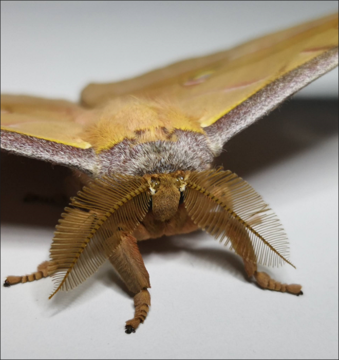
Up close and personal with a moth,

Caption: Antheraea pernyi Credit: University of Bristol

As for how this creature’s wings might provide inspiration for sound absorbing wallpaper, there’s this June 14, 2022 news item on phys.org, Note: A link has been removed,

Experts at the University of Bristol have discovered that the scales on moth wings act as excellent sound absorbers even when placed on an artificial surface.

The researchers, who recently discovered that moth wings offer acoustic protection from bat echolocation calls, have been studying whether their structure could inform better performing sound absorbing panels when not moving in free space.

A June 15, 2022 University of Bristol press release (also on EurekAlert but published on June 14, 2022), which originated the news item, delves further into the research, Note: Links have been removed,

Bats and moths have been involved in an acoustic arms race between predator and prey ever since bats evolved echolocation some 65 million years ago. Moths are under huge predation pressure from bats and have evolved a plethora of defences in their strive for survival, but it’s the scales, on a moth wing, that hold the key to transforming noise-cancelling technology.

Prof Marc Holderied, of Bristol’s School of Biological Sciences, said: “What we needed to know first, was how well these moth scales would perform if they were in front of an acoustically highly reflective surface, such as a wall.

“We also needed to find out how the mechanisms of absorption might change when the scales were interacting with this surface.”

Prof Holderied and his team tested this by placing small sections of moth wings on an aluminium disc, then systematically tested how orientation of the wing with respect to the incoming sound and the removal of scale layers affected absorption.

Remarkably, they found that moth wings proved to be excellent sound absorbers, even when on top of an acoustical solid substrate, with the wings absorbing as much as 87% of the incoming sound energy. The effect is also broadband and omnidirectional, covering a wide range of frequencies and sound incident angles.

“What is even more impressive is that the wings are doing this whilst being incredibly thin, with the scale layer being only 1/50th of the thickness of the wavelength of the sound that they are absorbing,” explained lead author Dr Thomas Neil. “This extraordinary performance qualifies the moth wing as a natural occurring acoustic absorbing metasurface, a material that has unique properties and capabilities, that are not possible to create using conventional materials.”

The potential to create ultrathin sound absorbing panels has huge implications in building acoustics. As cities get louder, the need for efficient non-intrusive sound mitigation solutions grows. Equally, these lightweight sound absorbing panels could have huge impacts on the travel industry, with any weight saving in planes, cars and trains increasing efficiency in these modes of transport, reducing fuel use and CO2 emissions.  

Now the scientists plan to replicate the sound absorbing performance by designing and building prototypes based on the sound absorbing mechanisms of the moth. The absorption that they have characterised in moth wing scales is all in the ultrasound frequency range, above that which humans can hear. Their next challenge is to design a structure that will work at lower frequencies whilst retaining the same ultrathin architecture employed by the moth.  

Prof Holderied concluded: “Moths are going to inspire the next generation of sound absorbing materials.

“New research has shown that one day it will be possible to adorn the walls of your house with ultrathin sound absorbing wallpaper, using a design that copies the mechanisms that gives moths stealth acoustic camouflage.”

Here’s link to and a citation for the paper,

Moth wings as sound absorber metasurface by Thomas R. Neil, Zhiyuan Shen, Daniel Robert, Bruce W. Drinkwater and Marc W. Holderied. Proceedings of the Royal Society A Mathematical Physical and Engineering Sciences DOI: https://doi.org/10.1098/rspa.2022.0046 Published:15 June 2022

This paper is open access.

Can I have a beer with those carbon quantum dots?

This research into using waste products from microbreweries comes from Québec, from a June 22, 2022 news item on ScienceDaily,

For a few years now, spent grain, the cereal residue from breweries, has been reused in animal feed. From now on, this material could also be used in nanotechnology! Professor Federico Rosei’s team at the Institut national de la recherche scientifique (INRS) has shown that microbrewery waste can be used as a carbon source to synthesize quantum dots. The work, done in collaboration with Claudiane Ouellet-Plamondon of the École de technologie supérieure (ÉTS), was published in the Royal Society of Chemistry’s journal RSC Advances

A June 22, 2022 Institut national de la recherche scientifique (INRS) news release (also on EurekAlert), which originated the news item, explains what quantum dots have to do with wastage from beer (Note: Links have been removed),

Often considered as “artificial atoms”, quantum dots are used in the transmission of light. With a range of interesting physicochemical properties, this type of nanotechnology has been successfully used as a sensor in biomedicine or as LEDs in next generation displays. But there is a drawback. Current quantum dots are produced with heavy and toxic metals like cadmium. Carbon is an interesting alternative, both for its biocompatibility and its accessibility.

An eco-responsible approach

The choice of brewery waste as a source material came from Daniele Benetti, a postdoctoral fellow at INRS, and Aurel Thibaut Nkeumaleu, the master’s student at ÉTS who conducted the work. Basically, they wanted to carry out various experiments using accessible materials. This is how the scientists came to collaborate with the Brasseurs de Montréal to obtain their cereal residues.

“The use of spent grain highlights both an eco-responsible approach to waste management and an alternative raw material for the synthesis of carbon quantum dots, from a circular economy perspective,” says Professor Rosei.

The advantage of using brewery waste as a source of carbon quantum dots is that it is naturally enriched with nitrogen and phosphorus. This avoids the need for pure chemicals.

“This research was a lot of fun, lighting up what we can do with the beer by-products,” says Claudiane Ouellet-Plamondon, Canada Research Chair in Sustainable Multifunctional Construction Materials at ÉTS. “Moreover, ÉTS is located on the site of the former Dow brewery, one of the main breweries in Quebec until the 1960s. So there is a historical and heritage link to this work.”

An accessible method

In addition to using biobased material, the research team wanted to show that it was possible to produce carbon quantum dots with common means. The scientists used a domestic microwave oven to carbonize the spent grain, resulting in a black powder. It was then mixed with distilled water and put back into the microwave oven. A passage in the centrifuge and advanced filtration allowed to obtain the quantum dots. Their finished product was able to detect and quantify heavy metals, as well as other contaminants that affect water quality, the environment and health. 

The next steps will be to characterize these carbon quantum dots from brewery waste, beyond proof of concept. The research team is convinced that this nanotechnology has the potential to become sophisticated detection sensors for various aqueous solutions, even in living cells.

About the study

The paper “Brewery spent grain derived carbon dots for metal sensing,” by Aurel Thibaut Nkeumaleu, Daniele Benetti, Imane Haddadou, Michael Di Mare, Claudiane Ouellet-Plamondon, and Federico Rosei, was published on April 14, 2022, in the Royal Society of Chemistry journal RSC Advances. The study was supported by the Natural Sciences and Engineering Research Council of Canada (NSERC), the Quebec Centre for Advanced Materials (QCAM) and the Canada Research Chairs.

About INRS
INRS is a university dedicated exclusively to graduate level research and training. Since its creation in 1969, INRS has played an active role in Québec’s economic, social, and cultural development and is ranked first for research intensity in Québec. INRS is made up of four interdisciplinary research and training centres in Québec City, Montréal, Laval, and Varennes, with expertise in strategic sectors: Eau Terre Environnement, Énergie Matériaux Télécommunications, Urbanisation Culture Société, and Armand-Frappier Santé Biotechnologie. The INRS community includes more than 1,500 students, postdoctoral fellows, faculty members, and staff.

Here’s a link to and a citation for the paper,

Brewery spent grain derived carbon dots for metal sensing by Aurel Thibaut Nkeumaleu, Daniele Benetti, Imane Haddadou, Michael Di Mare, Claudiane M. Ouellet-Plamondon and Federico Rosei. RSC Adv., 2022,12, 11621-11627 DOI: https://doi.org/10.1039/D2RA00048B First published: 14 Apr 2022

This paper is open access.