Tag Archives: flexible electronics

Self-assembiling gold nanowire inks for transparent electronics

A July 26, 2016 news item on phys.org describes the need for self-assembling, transparent inks,

Transparent electronics devices are present in today’s thin film displays, solar cells, and touchscreens. The future will bring flexible versions of such devices. Their production requires printable materials that are transparent and remain highly conductive even when deformed. Researchers at INM – Leibniz Institute for New Materials have combined a new self-assembling nano ink with an imprint process to create flexible conductive grids with a resolution below one micrometer.

A July 20, 2016 INM press release, which originated the news item, provides more detail,

To print the grids, an ink of gold nanowires is applied to a substrate. A structured stamp is pressed on the substrate and forces the ink into a pattern. “The nanowires are extremely thin and flexible; they adapt to any pattern of the stamp. During drying, the individual wires self-assemble and form larger, percolating bundles that form the grid,” explains Tobias Kraus from INM. The stamp is removed and the grid is treated in a plasma. “This compresses the bundles into conductive wires and results in a transparent, conductive grid. Depending on the geometry of the stamp, this simple method can shape any nano or microgrid,” says Kraus, head of the program division Structure Formation.

The thickness of the grid can be controlled via the gold concentration. “Only very small quantities of gold are needed to produce a conductive grid, far less than when using inks with spherical gold particles,” says Kraus. This makes the advantages of gold accessible for flexible electronics.

“Our results show self-assembly and imprint can be combined to efficiently produce transparent, conductive materials. We will transfer this insight to other metals in further studies,” says Kraus.

Here’s a link to and a citation for the paper,

Templated Self-Assembly of Ultrathin Gold Nanowires by Nanoimprinting for Transparent Flexible Electronics by Johannes H. M. Maurer, Lola González-García, Beate Reiser, Ioannis Kanelidis, and Tobias Kraus. Nano Lett., 2016, 16 (5), pp 2921–2925
DOI: 10.1021/acs.nanolett.5b04319 Publication Date (Web): March 17, 2016

Copyright © 2016 American Chemical Society

This paper is behind a paywall.

Printing in midair

Dexter Johnson’s May 16, 2016 posting on his Nanoclast blog (on the IEEE [Institute of Electrical and Electronics Engineers] website) was my first introduction to something wonder-inducing (Note: Links have been removed),

While the growth of 3-D printing has led us to believe we can produce just about any structure with it, the truth is that it still falls somewhat short.

Researchers at Harvard University are looking to realize a more complete range of capabilities for 3-D printing in fabricating both planar and freestanding 3-D structures and do it relatively quickly and on low-cost plastic substrates.

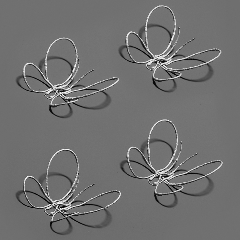
In research published in the journal Proceedings of the National Academy of Sciences (PNAS),  the researchers extruded a silver-nanoparticle ink and annealed it with a laser so quickly that the system let them easily “write” free-standing 3-D structures.

While this may sound humdrum, what really takes one’s breath away with this technique is that it can create 3-D structures seemingly suspended in air without any signs of support as though they were drawn there with a pen.

Laser-assisted direct ink writing allowed this delicate 3D butterfly to be printed without any auxiliary support structure (Image courtesy of the Lewis Lab/Harvard University)

Laser-assisted direct ink writing allowed this delicate 3D butterfly to be printed without any auxiliary support structure (Image courtesy of the Lewis Lab/Harvard University)

A May 16, 2016 Harvard University press release (also on EurekAlert) provides more detail about the work,

“Flat” and “rigid” are terms typically used to describe electronic devices. But the increasing demand for flexible, wearable electronics, sensors, antennas and biomedical devices has led a team at Harvard’s John A. Paulson School of Engineering and Applied Sciences (SEAS) and Wyss Institute for Biologically Inspired Engineering to innovate an eye-popping new way of printing complex metallic architectures – as though they are seemingly suspended in midair.

“I am truly excited by this latest advance from our lab, which allows one to 3D print and anneal flexible metal electrodes and complex architectures ‘on-the-fly,’ ” said Lewis [Jennifer Lewis, the Hansjörg Wyss Professor of Biologically Inspired Engineering at SEAS and Wyss Core Faculty member].

Lewis’ team used an ink composed of silver nanoparticles, sending it through a printing nozzle and then annealing it using a precisely programmed laser that applies just the right amount of energy to drive the ink’s solidification. The printing nozzle moves along x, y, and z axes and is combined with a rotary print stage to enable freeform curvature. In this way, tiny hemispherical shapes, spiral motifs, even a butterfly made of silver wires less than the width of a hair can be printed in free space within seconds. The printed wires exhibit excellent electrical conductivity, almost matching that of bulk silver.

When compared to conventional 3D printing techniques used to fabricate conductive metallic features, laser-assisted direct ink writing is not only superior in its ability to produce curvilinear, complex wire patterns in one step, but also in the sense that localized laser heating enables electrically conductive silver wires to be printed directly on low-cost plastic substrates.

According to the study’s first author, Wyss Institute Postdoctoral Fellow Mark Skylar-Scott, Ph.D., the most challenging aspect of honing the technique was optimizing the nozzle-to-laser separation distance.

“If the laser gets too close to the nozzle during printing, heat is conducted upstream which clogs the nozzle with solidified ink,” said Skylar-Scott. “To address this, we devised a heat transfer model to account for temperature distribution along a given silver wire pattern, allowing us to modulate the printing speed and distance between the nozzle and laser to elegantly control the laser annealing process ‘on the fly.’ ”

The result is that the method can produce not only sweeping curves and spirals but also sharp angular turns and directional changes written into thin air with silver inks, opening up near limitless new potential applications in electronic and biomedical devices that rely on customized metallic architectures.

Seeing is believing, eh?

Here’s a link to and a citation for the paper,

Laser-assisted direct ink writing of planar and 3D metal architectures by Mark A. Skylar-Scott, Suman Gunasekaran, and Jennifer A. Lewis. PNAS [Proceedings of the National Academy of Sciences] 2016 doi: 10.1073/pnas.1525131113

I believe this paper is open access.

A question: I wonder what conditions are necessary before you can 3D print something in midair? Much as I’m dying to try this at home, I’m pretty that’s not possible.

King Abdullah University of Science and Technology (Saudi Arabia) develops sensors from household materials

Researchers at the King Adbullah University of Science and Technology (KAUST) are developing sensors made of household materials according to a Feb. 19, 2016 KAUST news release (also on EurekAlert but dated Feb. 21, 2016),

Everyday materials from the kitchen drawer, such as aluminum foil, sticky note paper, sponges and tape, have been used by a team of electrical engineers from KAUST to develop a low-cost sensor that can detect external stimuli, including touch, pressure, temperature, acidity and humidity.

The sensor, which is called Paper Skin, performs as well as other artificial skin applications currently being developed while integrating multiple functions using cost-effective materials1.

“This work has the potential to revolutionize the electronics industry and opens the door to commercializing affordable high-performance sensing devices,” stated Muhammad Mustafa Hussain from the University’s Integrated Nanotechnology Lab, where the research was conducted.

Wearable and flexible electronics show promise for a variety of applications, such as wireless monitoring of patient health and touch-free computer interfaces. Current research in this direction employs expensive and sophisticated materials and processes.

The team used sticky note paper to detect humidity, sponges and wipes to detect pressure and aluminum foil to detect motion. Coloring a sticky note with an HB pencil allowed the paper to detect acidity levels, and aluminum foil and conductive silver ink were used to detect temperature differences.

The materials were put together into a simple paper-based platform that was then connected to a device that detected changes in electrical conductivity according to external stimuli.

Increasing levels of humidity, for example, increased the platform’s ability to store an electrical charge, or its capacitance. Exposing the sensor to an acidic solution increased its resistance, while exposing it to an alkaline solution decreased it. Voltage changes were detected with temperature changes. Bringing a finger closer to the platform disturbed its electromagnetic field, decreasing its capacitance.

The team leveraged the various properties of the materials they used, including their porosity, adsorption, elasticity and dimensions to develop the low-cost sensory platform. They also demonstrated that a single integrated platform could simultaneously detect multiple stimuli in real time.

Several challenges must be overcome before a fully autonomous, flexible and multifunctional sensory platform becomes commercially achievable, explained Hussain. Wireless interaction with the paper skin needs to be developed. Reliability tests also need to be conducted to assess how long the sensor can last and how good its performance is under severe bending conditions.

“The next stage will be to optimize the sensor’s integration on this platform for applications in medical monitoring systems. The flexible and conformal sensory platform will enable simultaneous real-time monitoring of body vital signs, such as heart rate, blood pressure, breathing patterns and movement,” Hussain said.

Here’s a link to and a citation for the paper,

Paper Skin Multisensory Platform for Simultaneous Environmental Monitoring by Joanna M. Nassar, Marlon D. Cordero, Arwa T. Kutbee, Muhammad A. Karimi, Galo A. Torres Sevilla, Aftab M. Hussain, Atif Shamim, and Muhammad M. Hussain. Advanced Materials Technologies DOI: 10.1002/admt.201600004 Article first published online: 19 FEB 2016

© 2016 WILEY-VCH Verlag GmbH & Co. KGaA, Weinheim

This appears to be an open access paper.

A wearable, stretchable body sensor based on chewing gum and carbon nanotubes

Any work which features a scientist chewing gum preparatory to using it for research purposes should be widely disseminated. In all the talk about science and equipment, it’s easy to forget that scientists are capable of great ingenuity with simple, every day materials. Also, the researchers are Canadian and based at the University of Manitoba. From a Dec. 2, 2015 American Chemical Society (ACS) news release (also on EurekAlert),

Body sensors, which were once restricted to doctors’ offices, have come a long way. They now allow any wearer to easily track heart rate, steps and sleep cycles around the clock. Soon, they could become even more versatile — with the help of chewing gum. Scientists report in the journal ACS Applied Materials & Interfaces a unique sensing device made of gum and carbon nanotubes that can move with your most bendable parts and track your breathing.

Most conventional sensors today are very sensitive and detect the slightest movement, but many are made out of metal. That means when they’re twisted or pulled too much, they stop working. But for sensors to monitor the full range of a body’s bending and stretching, they need a lot more give. To meet that need, some researchers have tried developing sensors using stretchy plastics and silicones. But what they gained in flexibility, they lost in sensitivity. Malcolm Xing and colleagues found a better solution right under their noses — and in their mouths.

To make their supple sensor, a team member chewed a typical piece of gum for 30 minutes, washed it with ethanol and let it sit overnight. The researchers then added a solution of carbon nanotubes, the sensing material. Simple pulling and folding coaxed the tubes to align properly. Human finger-bending and head-turning tests showed the material could keep working with high sensitivity even when strained 530 percent. The sensor also could detect humidity changes, a feature that could be used to track breathing, which releases water vapor with every exhale.

Here’s a link to and a citation for the paper,

Gum Sensor: A Stretchable, Wearable, and Foldable Sensor Based on Carbon Nanotube/Chewing Gum Membrane by Mohammad Ali Darabi, Ali Khosrozadeh, Quan Wang, and Malcolm Xing. ACS Appl. Mater. Interfaces, 2015, 7 (47), pp 26195–26205 DOI: 10.1021/acsami.5b08276 Publication Date (Web): November 2, 2015

Copyright © 2015 American Chemical Society

This paper is behind a paywall.

This video lets you see the gum/CNT material at work,

Enjoy!

Shape memory in a supercapacitor fibre for ‘smart’ textiles (wearable tech: 1 of 3)

Wearable technology seems to be quite trendy for a grouping not usually seen: consumers, fashion designers, medical personnel, manufacturers, and scientists.

The first in this informal series concerns a fibre with memory shape. From a Nov. 19, 2015 news item on Nanowerk (Note: A link has been removed),

Wearing your mobile phone display on your jacket sleeve or an EKG probe in your sports kit are not off in some distant imagined future. Wearable “electronic textiles” are on the way. In the journal Angewandte Chemie (“A Shape-Memory Supercapacitor Fiber”), Chinese researchers have now introduced a new type of fiber-shaped supercapacitor for energy-storage textiles. Thanks to their shape memory, these textiles could potentially adapt to different body types: shapes formed by stretching and bending remain “frozen”, but can be returned to their original form or reshaped as desired.

A Nov. 19, 2015 Wiley Publishers press release, which originated the news item, provides context and detail about the work,

Any electronic components designed to be integrated into textiles must be stretchable and bendable. This is also true of the supercapacitors that are frequently used for data preservation in static storage systems (SRAM). SRAM is a type of storage that holds a small amount of data that is rapidly retrievable. It is often used for caches in processors or local storage on chips in devices whose data must be stored for long periods without a constant power supply. Some time ago, a team headed by Huisheng Peng at Fudan University developed stretchable, pliable fiber-shaped supercapacitors for integration into electronic textiles. Peng and his co-workers have now made further progress: supercapacitor fibers with shape memory.

Any electronic components designed to be integrated into textiles must be stretchable and bendable. This is also true of the supercapacitors that are frequently used for data preservation in static storage systems (SRAM). SRAM is a type of storage that holds a small amount of data that is rapidly retrievable. It is often used for caches in processors or local storage on chips in devices whose data must be stored for long periods without a constant power supply.
Some time ago, a team headed by Huisheng Peng at Fudan University developed stretchable, pliable fiber-shaped supercapacitors for integration into electronic textiles. Peng and his co-workers have now made further progress: supercapacitor fibers with shape memory.

The fibers are made using a core of polyurethane fiber with shape memory. This fiber is wrapped with a thin layer of parallel carbon nanotubes like a sheet of paper. This is followed by a coating of electrolyte gel, a second sheet of carbon nanotubes, and a final layer of electrolyte gel. The two layers of carbon nanotubes act as electrodes for the supercapacitor. Above a certain temperature, the fibers produced in this process can be bent as desired and stretched to twice their original length. The new shape can be “frozen” by cooling. Reheating allows the fibers to return to their original shape and size, after which they can be reshaped again. The electrochemical performance is fully maintained through all shape changes.

Weaving the fibers into tissues results in “smart” textiles that could be tailored to fit the bodies of different people. This could be used to make precisely fitted but reusable electronic monitoring systems for patients in hospitals, for example. The perfect fit should render them both more comfortable and more reliable.

Here’s a link to and a citation for the paper,

A Shape-Memory Supercapacitor Fiber by Jue Deng, Ye Zhang, Yang Zhao, Peining Chen, Dr. Xunliang Cheng, & Prof. Dr. Huisheng Peng. Angewandte Chemie International Edition  DOI: 10.1002/anie.201508293  First published: 3 November 2015

This paper is behind a paywall.

Foldable glass (well, there’s some plastic too)

Michael Berger has written a fascinating Aug. 11, 2015 Nanowerk Spotlight article on folding glass,

Have you ever heard about foldable glass?

Exactly.

Glass is notorious for its brittleness. Although industry has developed ultra-thin (∼0.1 mm), flexible glass (like Corning’s Willow® Glass) that can be bent for applications liked curved TV and smartphone displays, fully foldable glass had not been demonstrated. Until now.

Khang [Dahl-Young Khang, an Associate Professor in the Department of Materials Science and Engineering at Yonsei University] and his group have now demonstrated substrate platforms of glass and plastics, which can be reversibly and repeatedly foldable at pre designed location(s) without any mechanical failure or deterioration in device performances.

“We have engineered the substrates to have thinned parts on which the folding deformation should occur,” Moon Jong Han, first author of the paper a graduate student in Khang’s lab, says. “This localizes the deformation strain on those thinned parts only.”

He adds that this approach to engineering substrates has another advantage regarding device materials: “There is no need to adopt any novel materials such as nanowires, carbon nanotubes, graphene, etc. Rather, all the conventional materials that have been used for high-performance devices can be directly applied on our engineered substrates.”

Intriguingly, even ITO (indium tin oxide), a very brittle transparent conducting oxide, can be used as electrode on this novel foldable glass platform.

What makes the approach especially intriguing is the ability to reverse the fold and that it doesn’t require special nanomaterials, such as carbon nanotubes, etc. From Berger’s Aug. 11, 2015 article,

The width of the thinned parts, the gap width, plays the key role in implementing dual foldability. The other key element is the asymmetric design of the gap width for the second folding.

The researchers achieved foldability, in part, by copying a technique used for folding mats and oriental hinge-less screens which have thinned areas to allow folding.

Here’s a link to and a citation for the paper,

Glass and Plastics Platforms for Foldable Electronics and Displays by Moon Jung Han and Dahl-Young Khang. Advanced Materials DOI: 10.1002/adma.201501060 First published: 21 July 2015

This paper is behind a paywall.

Berger’s article is not only fascinating, it is also illustrated with some images provided by the researchers.

‘Green’, flexible electronics with nanocellulose materials

Bendable or flexible electronics based on nanocellulose paper present a ‘green’ alternative to other solutions according to a May 20, 2015 American Chemical Society (ACS) news release (also on EurekAlert),

Technology experts have long predicted the coming age of flexible electronics, and researchers have been working on multiple fronts to reach that goal. But many of the advances rely on petroleum-based plastics and toxic materials. Yu-Zhong Wang, Fei Song and colleagues wanted to seek a “greener” way forward.

The researchers developed a thin, clear nanocellulose paper made out of wood flour and infused it with biocompatible quantum dots — tiny, semiconducting crystals — made out of zinc and selenium. The paper glowed at room temperature and could be rolled and unrolled without cracking.

(h’t Nanotechnology Now, May 20, 2015)

There’s no mention in the news release or abstract as to what material (wood, carrot, banana, etc.) was used to derive the nanocellulose. Regardless, here’s a link to and a citation for the paper,

Let It Shine: A Transparent and Photoluminescent Foldable Nanocellulose/Quantum Dot Paper by Juan Xue, Fei Song, Xue-wu Yin, Xiu-li Wang, and Yu-zhong Wang. ACS Appl. Mater. Interfaces, 2015, 7 (19), pp 10076–10079 DOI: 10.1021/acsami.5b02011 Publication Date (Web): May 4, 2015

Copyright © 2015 American Chemical Society

This paper is behind a paywall.

Fully textile-embedded transparent and flexible technology?

There are a lot of research teams jockeying for position in the transparent, flexible electrodes stakes (for anyone unfamiliar with the slang, I’m comparing the competition between various research teams to a horse race). A May 11, 2015 news item on Nanowerk describes work from an international collaboration at the University of Exeter (UK), Note: A link has been removed,

An international team of scientists, including Professor Monica Craciun from the University of Exeter, have pioneered a new technique to embed transparent, flexible graphene electrodes into fibres commonly associated with the textile industry.

The discovery could revolutionise the creation of wearable electronic devices, such as clothing containing computers, phones and MP3 players, which are lightweight, durable and easily transportable.

The international collaborative research, which includes experts from the Centre for Graphene Science at the University of Exeter, the Institute for Systems Engineering and Computers, Microsystems and Nanotechnology (INESC-MN) in Lisbon, the Universities of Lisbon and Aveiro in Portugal and the Belgian Textile Research Centre (CenTexBel), is published in the leading scientific journal Scientific Reports (“Transparent conductive graphene textile fibers”).

A May 11, 2015 University of Exeter press release (also on EurekAlert*), which originated the news item,  describes the current situation regarding transparent and flexible electrodes in textiles and how the research at Exeter improves the situation,

Professor Craciun, co-author of the research said: “This is a pivotal point in the future of wearable electronic devices. The potential has been there for a number of years, and transparent and flexible electrodes are already widely used in plastics and glass, for example. But this is the first example of a textile electrode being truly embedded in a yarn. The possibilities for its use are endless, including textile GPS systems, to biomedical monitoring, personal security or even communication tools for those who are sensory impaired.  The only limits are really within our own imagination.”

At just one atom thick, graphene is the thinnest substance capable of conducting electricity. It is very flexible and is one of the strongest known materials. The race has been on for scientists and engineers to adapt graphene for the use in wearable electronic devices in recent years.

This new research has identified that ‘monolayer graphene’, which has exceptional electrical, mechanical and optical properties, make it a highly attractive proposition as a transparent electrode for applications in wearable electronics. In this work graphene was created by a growth method called chemical vapour deposition (CVD) onto copper foil, using a state-of-the-art nanoCVD system recently developed by Moorfield.

The collaborative team established a technique to transfer graphene from the copper foils to a polypropylene fibre already commonly used in the textile industry.

Dr Helena Alves who led the research team from INESC-MN and the University of Aveiro said: “The concept of wearable technology is emerging, but so far having fully textile-embedded transparent and flexible technology is currently non-existing. Therefore, the development of processes and engineering for the integration of graphene in textiles would give rise to a new universe of commercial applications. “

Dr Ana Neves, Associate Research Fellow in Prof Craciun’s team from Exeter’s Engineering Department and former postdoctoral researcher at INESC added: “We are surrounded by fabrics, the carpet floors in our homes or offices, the seats in our cars, and obviously all our garments and clothing accessories. The incorporation of electronic devices on fabrics would certainly be a game-changer in modern technology.

“All electronic devices need wiring, so the first issue to be address in this strategy is the development of conducting textile fibres while keeping the same aspect, comfort and lightness. The methodology that we have developed to prepare transparent and conductive textile fibres by coating them with graphene will now open way to the integration of electronic devices on these textile fibres.”

Dr Isabel De Schrijver,an expert of smart textiles from CenTexBel said: “Successful manufacturing of wearable electronics has the potential for a disruptive technology with a wide array of potential new applications. We are very excited about the potential of this breakthrough and look forward to seeing where it can take the electronics industry in the future.”

Professor Saverio Russo, co-author and also from the University of Exeter, added: “This breakthrough will also nurture the birth of novel and transformative research directions benefitting a wide range of sectors ranging from defence to health care. “

In 2012 Professor Craciun and Professor Russo, from the University of Exeter’s Centre for Graphene Science, discovered GraphExeter – sandwiched molecules of ferric chloride between two graphene layers which makes a whole new system that is the best known transparent material able to conduct electricity.  The same team recently discovered that GraphExeter is also more stable than many transparent conductors commonly used by, for example, the display industry.

Here’s a link to and a citation for the paper,

Electron transport of WS2 transistors in a hexagonal boron nitride dielectric environment by Freddie Withers, Thomas Hardisty Bointon, David Christopher Hudson, Monica Felicia Craciun, & Saverio Russo. Scientific Reports 4, Article number: 4967 doi:10.1038/srep04967 Published 15 May 2014

Did they wait a year to announce the research or is this a second-go-round? In any event, it is an open access paper.

* Added EurekAlert link 1120 hours PDT on May 12, 2015.
Just how bendy are the new organic semiconductors?

In all the excitement about flexible electronics, an interesting question about performance, which seems to have been overlooked until now (how bendy are they?), is being answered by scientists, according to a May 5, 2015 University of Massachusetts at Amherst news release (also on EurekAlert),

A revolution is coming in flexible electronic technologies as cheaper, more flexible, organic transistors come on the scene to replace expensive, rigid, silicone-based semiconductors, but not enough is known about how bending in these new thin-film electronic devices will affect their performance, say materials scientists at the University of Massachusetts Amherst.

They are the first to apply inhomogeneous deformations, that is strain, to the conducting channel of an organic transistor and to understand the observed effects, says Reyes-Martinez [Marcos Reyes-Martinez], who conducted the series of experiments as part of his doctoral work.

As he explains, “This is relevant to today’s tech industry because transistors drive the logic of all the consumer electronics we use. In the screen on your smart phone, for example, every little pixel that makes up the image is turned on and off by hundreds of thousands or even millions of miniaturized transistors.”

“Traditionally, the transistors are rigid, made of an inorganic material such as silicon,” he adds. “We’re working with a crystalline semiconductorcalled rubrene, which is an organic, carbon-based material that has performance factors, such as charge-carrier mobility, surpassing those measured in amorphous silicon. Organic semiconductors are an interesting alternative to silicon because their properties can be tuned to make them easily processed, allowing them to coat a variety of surfaces, including soft substrates at relatively low temperatures. As a result, devices based on organic semiconductors are projected to be cheaper since they do not require high temperatures, clean rooms and expensive processing steps like silicon does.”

Until now, Reyes-Martinez notes, most researchers have focused on controlling the detrimental effects of mechanical deformation to atransistor’s electrical properties. But in their series of systematic experiments, the UMass Amherst team discovered that mechanical deformations only decrease performance under certain conditions, and actually can enhance or have no effect in other instances.

“Our goal was not only to show these effects, but to explain and understand them. What we’ve done istake advantage of the ordered structure of ultra-thin organic single crystals of rubrene to fabricate high-perfomance, thin-film transistors,” he says. “This is the first time that anyone has carried out detailed fundamental work at these length scales with a single crystal.”

Though single crystals were once thought to be too fragile for flexible applications, the UMass Amherst team found that crystals ranging in thickness from about 150 nanometers to 1 micrometer were thin enough to be wrinkled and applied to any elastomer substrate. Reyes-Martinez also notes, “Our experiments are especially important because they help scientists working on flexible electronic devices to determine performance limitations of new materials under extreme mechanical deformations, such as when electronic devices conform to skin.”

They developed an analytical model based on plate bending theoryto quantifythe different local strains imposed on the transistor structure by the wrinkle deformations. Using their model they are able to predict how different deformations modulate charge mobility, which no one had quantified before, Reyes-Martinez notes.

These contributions “represent a significant step forward in structure-function relationships in organic semiconductors, critical for the development of the next generation of flexible electronic devices,” the authors point out.

Here’s a link to and a citation for the paper,

Rubrene crystal field-effect mobility modulation via conducting channel wrinkling by Marcos A. Reyes-Martinez, Alfred J. Crosby,  & Alejandro L. Briseno. Nature Communications 6, Article number: 6948 doi:10.1038/ncomms7948 Published 05 May 2015

This is an open access paper.

Hyper stretchable nanogenerator

There’s a lot of talk about flexibility, stretchability and bendability in electronics and the latest is coming from Korea. An April 13, 2015 Korea Advanced Institute for Science and Technology (KAIST) news release on EurekAlert describes the situation and the Korean scientists’ most recent research into stretchable electronics,

A research team led by Professor Keon Jae Lee of the Department of Materials Science and Engineering at the Korea Advanced Institute of Science and Technology (KAIST) has developed a hyper-stretchable elastic-composite energy harvesting device called a nanogenerator.

Flexible electronics have come into the market and are enabling new technologies like flexible displays in mobile phone, wearable electronics, and the Internet of Things (IoTs). However, is the degree of flexibility enough for most applications? For many flexible devices, elasticity is a very important issue. For example, wearable/biomedical devices and electronic skins (e-skins) should stretch to conform to arbitrarily curved surfaces and moving body parts such as joints, diaphragms, and tendons. They must be able to withstand the repeated and prolonged mechanical stresses of stretching. In particular, the development of elastic energy devices is regarded as critical to establish power supplies in stretchable applications. Although several researchers have explored diverse stretchable electronics, due to the absence of the appropriate device structures and correspondingly electrodes, researchers have not developed ultra-stretchable and fully-reversible energy conversion devices properly.

Recently, researchers from KAIST and Seoul National University (SNU) have collaborated and demonstrated a facile methodology to obtain a high-performance and hyper-stretchable elastic-composite generator (SEG) using very long silver nanowire-based stretchable electrodes. Their stretchable piezoelectric generator can harvest mechanical energy to produce high power output (~4 V) with large elasticity (~250%) and excellent durability (over 104 cycles). These noteworthy results were achieved by the non-destructive stress- relaxation ability of the unique electrodes as well as the good piezoelectricity of the device components. The new SEG can be applied to a wide-variety of wearable energy-harvesters to transduce biomechanical-stretching energy from the body (or machines) to electrical energy.

Professor Lee said, “This exciting approach introduces an ultra-stretchable piezoelectric generator. It can open avenues for power supplies in universal wearable and biomedical applications as well as self-powered ultra-stretchable electronics.”

Here’s a link to and a citation for the paper,

A Hyper-Stretchable Elastic-Composite Energy Harvester by Chang Kyu Jeong, Jinhwan Lee, Seungyong Han, Jungho Ryu, Geon-Tae Hwang, Dae Yong Park, Jung Hwan Park, Seung Seob Lee, Mynghwan Byun, Seung Hwan Ko, and Keon Jae Lee. Advanced Materials DOI: 10.1002/adma.201500367 30 March 2015Full

This paper is behind a paywall.

The researchers have prepared a short video (22 secs. and silent),