Tag Archives: FET Graphene Flagship project

Graphene-based neural probes

I have two news bits (dated almost one month apart) about the use of graphene in neural probes, one from the European Union and the other from Korea.

European Union (EU)

This work is being announced by the European Commission’s (a subset of the EU) Graphene Flagship (one of two mega-funding projects announced in 2013; 1B Euros each over ten years for the Graphene Flagship and the Human Brain Project).

According to a March 27, 2017 news item on ScienceDaily, researchers have developed a graphene-based neural probe that has been tested on rats,

Measuring brain activity with precision is essential to developing further understanding of diseases such as epilepsy and disorders that affect brain function and motor control. Neural probes with high spatial resolution are needed for both recording and stimulating specific functional areas of the brain. Now, researchers from the Graphene Flagship have developed a new device for recording brain activity in high resolution while maintaining excellent signal to noise ratio (SNR). Based on graphene field-effect transistors, the flexible devices open up new possibilities for the development of functional implants and interfaces.

The research, published in 2D Materials, was a collaborative effort involving Flagship partners Technical University of Munich (TU Munich; Germany), Institut d’Investigacions Biomèdiques August Pi i Sunyer (IDIBAPS; Spain), Spanish National Research Council (CSIC; Spain), The Biomedical Research Networking Center in Bioengineering, Biomaterials and Nanomedicine (CIBER-BBN; Spain) and the Catalan Institute of Nanoscience and Nanotechnology (ICN2; Spain).
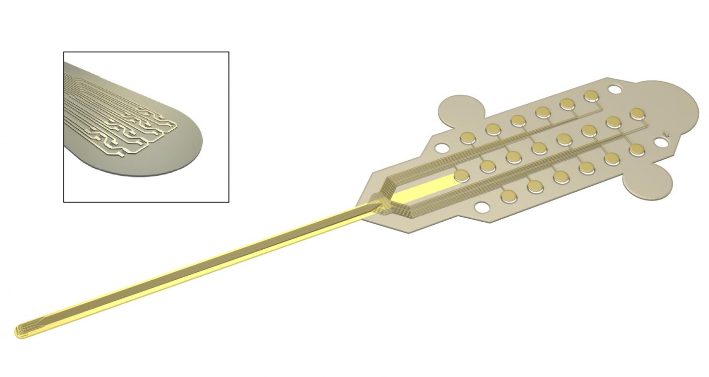
Caption: Graphene transistors integrated in a flexible neural probe enables electrical signals from neurons to be measured with high accuracy and density. Inset: The tip of the probe contains 16 flexible graphene transistors. Credit: ICN2

A March 27, 2017 Graphene Flagship press release on EurekAlert, which originated the news item, describes the work,  in more detail,

The devices were used to record the large signals generated by pre-epileptic activity in rats, as well as the smaller levels of brain activity during sleep and in response to visual light stimulation. These types of activities lead to much smaller electrical signals, and are at the level of typical brain activity. Neural activity is detected through the highly localised electric fields generated when neurons fire, so densely packed, ultra-small measuring devices is important for accurate brain readings.

The neural probes are placed directly on the surface of the brain, so safety is of paramount importance for the development of graphene-based neural implant devices. Importantly, the researchers determined that the graphene-based probes are non-toxic, and did not induce any significant inflammation.

Devices implanted in the brain as neural prosthesis for therapeutic brain stimulation technologies and interfaces for sensory and motor devices, such as artificial limbs, are an important goal for improving quality of life for patients. This work represents a first step towards the use of graphene in research as well as clinical neural devices, showing that graphene-based technologies can deliver the high resolution and high SNR needed for these applications.

First author Benno Blaschke (TU Munich) said “Graphene is one of the few materials that allows recording in a transistor configuration and simultaneously complies with all other requirements for neural probes such as flexibility, biocompability and chemical stability. Although graphene is ideally suited for flexible electronics, it was a great challenge to transfer our fabrication process from rigid substrates to flexible ones. The next step is to optimize the wafer-scale fabrication process and improve device flexibility and stability.”

Jose Antonio Garrido (ICN2), led the research. He said “Mechanical compliance is an important requirement for safe neural probes and interfaces. Currently, the focus is on ultra-soft materials that can adapt conformally to the brain surface. Graphene neural interfaces have shown already great potential, but we have to improve on the yield and homogeneity of the device production in order to advance towards a real technology. Once we have demonstrated the proof of concept in animal studies, the next goal will be to work towards the first human clinical trial with graphene devices during intraoperative mapping of the brain. This means addressing all regulatory issues associated to medical devices such as safety, biocompatibility, etc.”
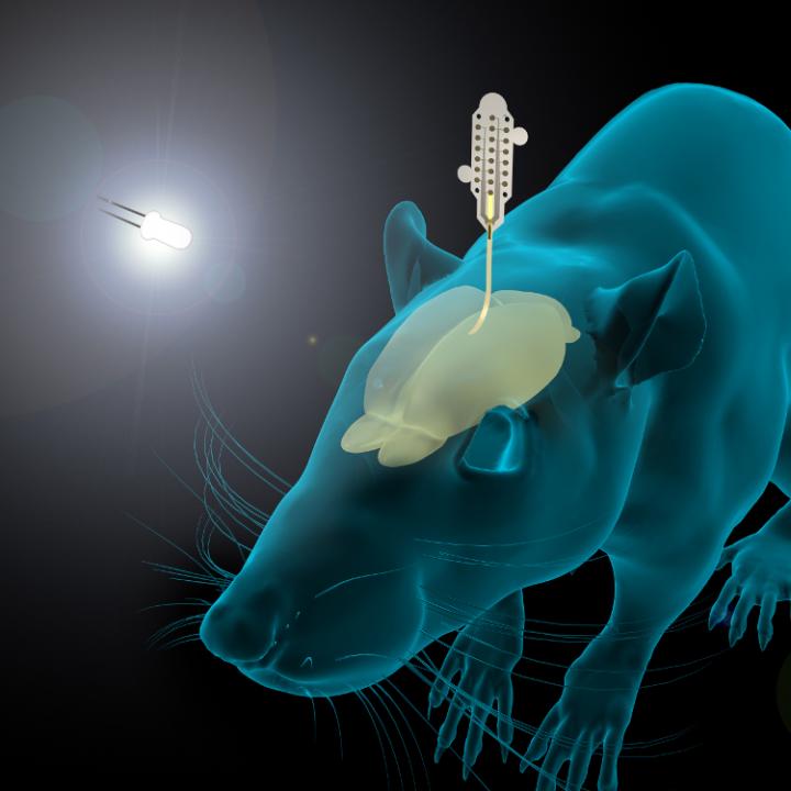
Caption: The graphene-based neural probes were used to detect rats’ responses to visual stimulation, as well as neural signals during sleep. Both types of signals are small, and typically difficult to measure. Credit: ICN2

Here’s a link to and a citation for the paper,

Mapping brain activity with flexible graphene micro-transistors by Benno M Blaschke, Núria Tort-Colet, Anton Guimerà-Brunet, Julia Weinert, Lionel Rousseau, Axel Heimann, Simon Drieschner, Oliver Kempski, Rosa Villa, Maria V Sanchez-Vives. 2D Materials, Volume 4, Number 2 DOI https://doi.org/10.1088/2053-1583/aa5eff Published 24 February 2017

© 2017 IOP Publishing Ltd

This paper is behind a paywall.

Korea

While this research from Korea was published more recently, the probe itself has not been subjected to in vivo (animal testing). From an April 19, 2017 news item on ScienceDaily,

Electrodes placed in the brain record neural activity, and can help treat neural diseases like Parkinson’s and epilepsy. Interest is also growing in developing better brain-machine interfaces, in which electrodes can help control prosthetic limbs. Progress in these fields is hindered by limitations in electrodes, which are relatively stiff and can damage soft brain tissue.

Designing smaller, gentler electrodes that still pick up brain signals is a challenge because brain signals are so weak. Typically, the smaller the electrode, the harder it is to detect a signal. However, a team from the Daegu Gyeongbuk Institute of Science & Technology [DGIST} in Korea developed new probes that are small, flexible and read brain signals clearly.

This is a pretty interesting way to illustrate the research,

Caption: Graphene and gold make a better brain probe. Credit: DGIST

An April 19, 2017 DGIST press release (also on EurekAlert), which originated the news item, expands on the theme (Note: A link has been removed),

The probe consists of an electrode, which records the brain signal. The signal travels down an interconnection line to a connector, which transfers the signal to machines measuring and analysing the signals.

The electrode starts with a thin gold base. Attached to the base are tiny zinc oxide nanowires, which are coated in a thin layer of gold, and then a layer of conducting polymer called PEDOT. These combined materials increase the probe’s effective surface area, conducting properties, and strength of the electrode, while still maintaining flexibility and compatibility with soft tissue.

Packing several long, thin nanowires together onto one probe enables the scientists to make a smaller electrode that retains the same effective surface area of a larger, flat electrode. This means the electrode can shrink, but not reduce signal detection. The interconnection line is made of a mix of graphene and gold. Graphene is flexible and gold is an excellent conductor. The researchers tested the probe and found it read rat brain signals very clearly, much better than a standard flat, gold electrode.

“Our graphene and nanowires-based flexible electrode array can be useful for monitoring and recording the functions of the nervous system, or to deliver electrical signals to the brain,” the researchers conclude in their paper recently published in the journal ACS Applied Materials and Interfaces.

The probe requires further clinical tests before widespread commercialization. The researchers are also interested in developing a wireless version to make it more convenient for a variety of applications.

Here’s a link to and a citation for the paper,

Enhancement of Interface Characteristics of Neural Probe Based on Graphene, ZnO Nanowires, and Conducting Polymer PEDOT by Mingyu Ryu, Jae Hoon Yang, Yumi Ahn, Minkyung Sim, Kyung Hwa Lee, Kyungsoo Kim, Taeju Lee, Seung-Jun Yoo, So Yeun Kim, Cheil Moon, Minkyu Je, Ji-Woong Choi, Youngu Lee, and Jae Eun Jang. ACS Appl. Mater. Interfaces, 2017, 9 (12), pp 10577–10586 DOI: 10.1021/acsami.7b02975 Publication Date (Web): March 7, 2017

Copyright © 2017 American Chemical Society

This paper is behind a paywall.
Converting light to electricity at femto speeds

This is a pretty remarkable (to me anyway) piece of research on speeding up the process of converting light to electricity. From an April 14, 2015 Institute of Photonic Science press release (also on EurekAlert but dated April 15, 2015),

The efficient conversion of light into electricity plays a crucial role in many technologies, ranging from cameras to solar cells. It also forms an essential step in data communication applications, since it allows for information carried by light to be converted into electrical information that can be processed in electrical circuits. Graphene is an excellent material for ultrafast conversion of light to electrical signals, but so far it was not known how fast graphene responds to ultrashort flashes of light.

The new device that the researchers developed is capable of converting light into electricity in less than 50 femtoseconds (a twentieth of a millionth of a millionth of a second). To do this, the researchers used a combination of ultrafast pulse-shaped laser excitation and highly sensitive electrical readout. As Klaas-Jan Tielrooij comments, “the experiment uniquely combined the ultrafast pulse shaping expertise obtained from single molecule ultrafast photonics with the expertise in graphene electronics. Facilitated by graphene’s nonlinear photo-thermoelectric response, these elements enabled the observation of femtosecond photodetection response times.”

The ultrafast creation of a photovoltage in graphene is possible due to the extremely fast and efficient interaction between all conduction band carriers in graphene. This interaction leads to a rapid creation of an electron distribution with an elevated electron temperature. Thus, the energy absorbed from light is efficiently and rapidly converted into electron heat. Next, the electron heat is converted into a voltage at the interface of two graphene regions with different doping. This photo-thermoelectric effect turns out to occur almost instantaneously, thus enabling the ultrafast conversion of absorbed light into electrical signals. As Prof. van Hulst states, “it is amazing how graphene allows direct non-linear detecting of ultrafast femtosecond (fs) pulses”.

The results obtained from the findings of this work, which has been partially funded by the EC Graphene Flagship, open a new pathway towards ultra-fast optoelectronic conversion. As Prof. Koppens comments, “Graphene photodetectors keep showing fascinating performances addressing a wide range of applications”.

Here’s a link to and a citation for the paper,

Generation of photovoltage in graphene on a femtosecond timescale through efficient carrier heating by K. J. Tielrooij, L. Piatkowski, M. Massicotte, A. Woessner, Q. Ma, Y. Lee,  K. S. Myhro, C. N. Lau, P. Jarillo-Herrero, N. F. van Hulst & F. H. L. Koppens. Nature Nanotechnology (2015) doi:10.1038/nnano.2015.54 Published online 13 April 2015

This paper is behind a paywall but there is a free preview via ReadCube Access.

Of graphene cities and Manchester (UK)

I have expressed great admiration for the graphene publicity effort (mentioned in this Feb. 21, 2012 posting and elsewhere) put on by the UK during the run up to its European Commission award of a 1B Euro research prize in January 2013 (mentioned in my Jan. 28, 2013 posting). Officially, the award was given to the Graphene FET (future and emerging technologies) flagship project consortium headed by Chalmers University (Sweden).

The University of Manchester, a member of the consortium, has been active in graphene research and commercialization in the UK, from my Feb. 19, 2013 posting,

The University of Manchester (UK) has a particular interest in graphene as the material was isolated by future Nobel Prize winners, Andre Gheim and Kostya (Konstantin) Novoselov in the university’s laboratories. There’s a Feb. 18, 2013 news item on Nanowerk highlighting the university’s past and future role in the development of graphene on the heels of the recent research bonanza,

The European Commission has announced that it is providing 1bn euros over 10 years for research and development into graphene – the ‘wonder material’ isolated at The University of Manchester by Nobel Prize winners Professors Andre Geim and Kostya Novoselov.

The University is very active in technology transfer and has an excellent track-record of spinning out technology, but some think that the University has taken a different view when it comes to patenting and commercialising graphene. Others have expressed a broader concern about British Industry lagging behind in the graphene ‘race’, based upon international ‘league tables’ of numbers of graphene patents.

Manchester is the site for one of two graphene institutions in the UK as per my Jan. 14, 2013 posting titled, National Graphene Institute at the UK’s University of Manchester. The other is in Cambridge as per my Jan. 24, 2013 posting titled, Another day, another graphene centre in the UK as the Graphene flagship consortium’s countdown begins.

The latest item ‘graphene & UK’ (Manchester) item I’m featuring here is a May 12, 2014 news item on Azonano titled, ‘Graphene City’ Can be a Model for Commercialising Scientific Discoveries (Note: A link has been removed),

This is a blog [posting] by James Baker, Business Director for Graphene@Manchester. As the government announces further support for the UK’s emerging graphene industry, James Baker from the National Graphene Institute says the emerging concept of a ‘graphene city’ can be a UK model for commercialising new scientific discoveries.

After a few fits and starts, I traced the news item to a May 7, 2014 posting on the University of Manchester’s [Manchester] Policy Blogs: Science and Technology blog,

Announcing new investments into graphene commercialisation in March’s [2014] Budget, Chancellor George Osborne described the material as a “great British discovery that we should break the habit of a lifetime with and commercially develop in Britain”.

As the new business director for the National Graphene Institute (NGI), which has its new £61m building opening here at the University next year, I obviously couldn’t agree more.

I first came across graphene in my previous job at defence giant BAE Systems where I was in charge of technology collaboration programmes. We ran a number of ‘futures’ workshops where the aim was to get senior executives to think about how the wider world might look in 20 years time.

In defence there has been much debate about the need for a coherent defence industrial strategy to ensure we have the necessary skills and industrial capabilities for the future, and it was through these sessions that a wider dialogue around technologies such as graphene as a potential ‘disruptive’ capability started to emerge.

Whether it’s helping develop new lightweight components for aircraft or battery packs for soldiers, or developing flexible touch screens for the specialist gadget market, graphene has a vast array of potential uses.

My role is to sign up potential industrial partners who want to collaborate with The University of Manchester and take the graphene science to a higher maturity and onto commercialisation. We are looking for partners across a range of sectors who want to operate in this environment in an open, shared and collaborative way.

The vision of creating a ‘graphene city’ in the 21st century can be compared with Manchester in the 19th century when economic activity and innovation developed largely in the absence of the state.

If you are interested in graphene commercialization in the UK, this posting offers some insight into how at least one person involved in this process views the possibilities.

Graphene hype; the emerging story in an interview with Carla Alvial Palavicino (University of Twente, Netherlands)

i’m delighted to be publishing this interview with Carla Alvial Palavicino, PhD student at the University of Twente (Netherlands), as she is working on the topicof  graphene ‘hype’. Here’s a bit more about the work from her University of Twente webpage (Note: A link has been removed),

From its origins the field of nanotechnology has been populated of expectations. Pictured as “the new industrial revolution” the economic promise holds strong, but also nanotechnologies as a cure for almost all the human ills, sustainers of future growth, prosperity and happiness. In contrast to these promises, the uncertainties associated to the introduction of such a new and revolutionary technology, and mainly risks of nanomaterials, have elicited concerns among governments and the public. Nevertheless, the case of the public can be characterized as concerns about concerns, based on the experience of previous innovations (GMO, etc.).

Expectations, both as promises and concerns, have played and continue playing a central role in the “real-time social and political constitution of nanotechnology” (Kearnes and Macnaghten 2006). A circulation of visions, promises and concerns in observed in the field, from the broadly defined umbrella promises to more specific expectations, and references to grand challenges as moral imperatives. These expectations have become such an important part of the social repertoire of nano applications that we observe the proliferation of systematic and intentional modes of expectation building such as roadmaps, technology assessment, etc.; as well as a considerable group of reports on risk, concerns, and ethical and social aspects. This different modes of expectation building (Konrad 2010) co-exist and contribute to the articulation of the nano field.

This project seeks to identify, characterize and contextualize the existing modes of expectations building, being those intentional (i.e. foresight, TA, etc.) or implicit in arenas of public discourse, associated to ongoing and emerging social processes in the context of socio-technical change.

This dynamics are being explored in relation to the new material graphene.

Before getting to the interview, here’s Alvial Palavicino’s biography,

Carla Alvial Palavicino has a bachelor degree in Molecular Biology Engineering, School of Science, University of Chile, Chile and a Master’s degree on Sustainability Sciences, Graduate School of Frontier Science, University of Tokyo, Japan. She has worked in technology transfer and more recently, in Smart Grids and local scale renewable energy provision.

Finally, here’s the interview (Note: At the author’s request, there have been some grammatical changes made to conform with Canadian English.),

  • What is it that interests you about the ‘hype’ that some technologies receive and how did you come to focus on graphene in particular?

My research belongs to a field called the Sociology of Expectations, which deals with the role of promises, visions, concerns and ideas of the future in the development of technologies, and how these ideas actually affect people’s strategies in technology development. Part of the dynamic found for these expectations are hype-disappointment cycles, much like the ones the Gartner Group uses. And hype has become an expectation itself; people expect that there will be too many promises and some, maybe many of them are not going to be fulfilled, followed by disappointment.

I came to know about graphene because, initially, I was broadly interested in nanoelectronics (my research project is part of NanoNextNL a large Dutch Nano research programme), due to the strong future orientation in the electronics industry. The industry has been organizing, and continues to organize around the promise of Moore’s law for more than 50 years! So I came across graphene as thriving to some extent on the expectations around the end of Moore’s law and because simply everybody was talking about it as the next big thing! Then I thought, this is a great opportunity to investigate hype in real-time

  • Is there something different about the hype for graphene or is this the standard ‘we’ve found a new material and it will change everything’?

I guess with every new technology and new material you find a portion of genuine enthusiasm which might lead to big promises. But that doesn’t necessarily turn into big hype. One thing is that all hype is not the same and you might have technologies that disappeared after the hype such as High Temperature Semiconductors, or technologies that go through a number of hype cycles and disappointment cycles throughout their development (for example, Fuel Cells). Now with graphene what you certainly have is very ‘loud’ hype – the amount of attention it has received in so little time is extraordinary. If that is a characteristic of graphene or a consequence of the current conditions in which the hype has been developed, such as faster ways of communication (social media for example) or different incentives for science and innovation well, this is part of what I am trying to find out.

Quite clearly, the hype in graphene seems to be more ‘reflexive’ than others, that is, people seem to be more conscious about hype now. We have had the experience with carbon nanotubes only recently and scientist, companies and investors are less naïve about what can be expected of the technology, and what needs to be done to move it forward ‘in the right direction’. And they do act in ways that try to soften the slope of the hype-disappointment curve. Having said that, actors [Ed. Note: as in actor-network theory] are also aware of how they can take some advantage of the hype (for funding, investment, or another interest), how to make use of it and hopefully leave safely, before disappointment. In the end, it is rather hard to ask accountability of big promises over the long-term.

  • In the description of your work you mention intentional and implicit modes of building expectations, could explain the difference between the two?

One striking feature of technology development today is that we found more and more activities directed at learning about, assess, and shaping the future, such as forecasts, foresights, Delphi, roadmaps and so on. There are even specialized future actors such as consultancy organisations or foresight experts,  Cientifica among them. And these formalized ways of anticipating  the future are expected to be performative by those who produce them and use them, that is, influence the way the future – and the present- turns out. But this is not a linear story, it’s not like 100% of a roadmap can be turned practice (not even for the ITRS roadmap [Ed. Note: International Technology Roadmap for Semi-conductors] that sustains Moore’s law, some expectations change quite radically between editions of the roadmap). Besides that, there are other forms of building expectations which are embedded in practices around new technologies. Think of the promises made in high profile journals or grant applications; and of expectations incorporated in patents and standards. All these embody particular forms and directions for the future, and exclude others. These are implicit forms of expectation-building, even if not primarily intended as such. These forms are shaped by particular expectations which themselves shape further development. So, in order to understand how these practices, both intentional and implicit, anticipate futures you need to look at the interplay between the various types.

  • Do you see a difference internationally with regard to graphene hype? Is it more prevalent in Europe than in the North America? Is it particularly prevalent in some jurisdiction, e.g. UK?

I think the graphene ‘hype’ has been quite global, but it is moving to different communities, or actors groups, as Tim Harper from Cientifica has mentioned in his recent report about graphene

What is interesting in relation to the different ‘geographical’ responses to graphene is that they exemplify nicely how a big promise (graphene, in this case) is connected to other circulating visions, expectations or concerns. In the case of the UK, the *Nobel prize on Graphene and the following investment was connected to the idea of a perceived crisis of innovation in the country. Thus, the decision to invest in graphene was presented and discussed in reference to global competitiveness, showing a political commitment for science and innovation that was in doubt at that time.

In the European case with its *Graphene flagship, something similar happened. While there is no doubt of the scientific excellence of the flagship project, the reasons why it finally became a winner in the flagship competition might have been related to the attention on graphene. The project itself started quite humbly, and it differed from the other flagship proposals that were much more oriented towards economic or societal challenges. But the attention graphene received after the Nobel Prize, plus the engagement of some large companies, helped to frame the project in terms of its economic profitability.  And. this might have helped to bring attention and make sense of the project in the terms the European Commission was interested in.

In contrast, if you think of the US, the hype has been there (the number of companies engaged in graphene research is only increasing) but it has not had a big echo in policy. One of the reasons might be because this idea of global competition and being left behind is not so present in the US. And in the case of Canada for example, graphene has been taken up by the graphite (mining) community, which is a very local feature.

So answering your questions, the hype has been quite global and fed in a global way (developments in one place resonate in the other) but different geographical areas have reacted in relation to their contingent expectations to what this hype dynamic provided.

  • What do you think of graphene?

I think it’s the new material with more YouTube videos (this one is particularly good in over promising for example)  and the coolest superhero (Mr G from the Flagship). But seriously,  I often get asked that question when I do interviews with actors in the field, since they are curious to learn about the outsider perspective. But to be honest I try to remain as neutral and distant as possible regarding my research object… and not getting caught in the hype!

Thanks so much for a fascinating interview Carla and I very much appreciate the inclusion of Canada in your response to the question about the international response to graphene hype. (Here are three of my postings on graphite and mining in Canada: Canada’s contribution to graphene research: big graphite flakes [Feb. 6, 2012]; A ‘graphite today, graphene tomorrow’ philosophy from Focus Graphite [April 17, 2013[; and Lomiko’s Quatre Milles graphite flakes—pure and ultra pure [April 17, 2013] There are others you can find by searching ‘graphite’ in the blog’s search box.)

* For anyone curious about the Nobel prize and graphene, there’s this Oct.7, 2010 posting. Plus, the Graphene Flagship was one of several projects competing for one of the two 1B Euro research prizes awarded in January 2013 (the win is mentioned in my Jan. 28, 2013 posting).

Merry Christmas, Happy New Year, and Happy Holidays to all!

Another day, another graphene centre in the UK as the Graphene flagship consortium’s countdown begins

The University of Cambridge has announced a Cambridge Graphene Centre due to open by the end of 2013 according to a Jan. 24, 2012 news item on Nanowerk,

The Cambridge Graphene Centre will start its activities on February 1st 2013, with a dedicated facility due to open at the end of the year. Its objective is to take graphene to the next level, bridging the gap between academia and industry. It will also be a shared research facility with state-of-the-art equipment, which any scientist researching graphene will have the opportunity to use.

The University of Cambridge Jan. 24, 2013 news release, which originated the news item, describes the plans for graphene research and commercialization,

The first job for those working in the Cambridge Graphene Centre will be to find ways of manufacturing and optimising graphene films, dispersions and inks so that it can be used to good effect.

Professor Andrea Ferrari, who will be the Centre’s Director, said: “We are now in the second phase of graphene research, following the award of the Nobel Prize to Geim and Novoselov. That means we are targeting applications and manufacturing processes, and broadening research to other two-dimensional materials and hybrid systems. The integration of these new materials could bring a new dimension to future technologies, creating faster, thinner, stronger, more flexible broadband devices.”

One such project, led by Dr Stephan Hofmann, a Reader and specialist in nanotechnology, will look specifically at the manufacturability of graphene and other, layered, 2D materials. At the moment, sheets of graphene that are just one atom thick are difficult to grow in a controllable manner, manipulate, or connect with other materials.

Dr Hofmann’s research team will focus on a growth method called chemical vapour deposition (CVD), which has already opened up other materials, such as diamond, carbon nanotubes and gallium nitride, to industrial scale production.

“The process technology will open up new horizons for nanomaterials, built layer by layer, which means that it could lead to an amazing range of future devices and applications,” Dr Hofmann said.

The Government funding for the Centre is complemented by strong industrial support, worth an additional £13 million, from over 20 partners, including Nokia, Dyson, Plastic Logic, Philips and BaE systems. A further £11M of European Research Council funding will support activities with the Graphene Institute in Manchester, and Lancaster University. [emphasis mine]

Its work will focus on taking graphene from a state of raw potential to a point where it can revolutionise flexible, wearable and transparent electronics. The Centre will target the manufacture of graphene on an industrial scale, and applications in the areas of flexible electronics, energy, connectivity and optoelectronics.

Professor Yang Hao, of Queen Mary, University of London, will lead Centre activities targeting connectivity, so that graphene can be integrated into networked devices, with the ultimate vision of creating an “internet of things”.

Professor Clare Grey, from Cambridge’s Department of Chemistry, will lead the activities targeting the use of graphene in super-capacitors and batteries for energy storage. The research could, ultimately, provide a more effective energy storage for electric vehicles, storage on the grid, as well as boosting the energy storage possibilities of personal devices such as MP3 players and mobile phones.

The announcement of a National Graphene Institute in Manchester was mentioned in my Jan. 14, 2013 posting and both the University of Manchester and the Lancaster University are part of the Graphene Flagship consortium along with the University of Cambridge and Sweden’s Chalmers University, which is the lead institution, and others competing against three other Flagship projects for one of two 1B Euro prizes.

These two announcements (Cambridge Graphene Centre and National Graphene Institute come at an interesting time, the decision as to which two projects will receive 1B Euros for research is being announced Jan. 28, 2013 in Brussels, Belgium. The Jan. 15, 2013 article by Frank Jordans on the R&D website provides a few more details,

Teams of scientists from across the continent [Europe] are vying for a funding bonanza that could see two of them receive up to €1 billion ($1.33 billion) over 10 years to keep Europe at the cutting edge of technology.

The contest began with 26 proposals that were whittled down to six last year. Just four have made it to the final round.

They include a plan to develop digital guardian angels that would keep people safe from harm; a massive data-crunching machine to simulate social, economic and technological change on our planet; an effort to craft the most accurate computer model of the human brain to date; and a team working to find better ways to produce and employ graphene—an ultra-thin material that could revolutionize manufacturing of everything from airplanes to computer chips.

Jordans’ article goes on to further explain the reasoning for this extraordinary contest. All four groups must be highly focused on Monday’s (Jan. 28, 2013) announcement from EU (European Union) officials, after all, two prizes and four competitors means that the odds of winning are 50/50. Good luck!

Latest on UK and graphene

The Brits are at it again with another graphene funding announcement, from the Dec. 28, 2012 news item on Azonano,

The Chancellor of the Exchequer, George Osborne MP, today announced £21.5 million of capital investment to commercialise graphene, one of the thinnest, lightest, strongest and most conductive materials to have been discovered, marked by the 2010 Nobel Prize in Physics as one of the world’s most ground breaking scientific achievements.

Three research projects at Imperial will share the Engineering and Physical Sciences Research Council (EPSRC) funding as part of a new programme with a number of industrial partners, including aeroplane manufacturer Airbus. The scientists receiving the grant hope to develop graphene technologies that will contribute to the UK economy and can be applied by industries around the world.

The Imperial College of London Dec. 27, 2012 news release, which originated the item, describes how the college’s £4.5M award will be used for three of its graphene projects,

In one project worth £1.35 million, led by Professor Tony Kinloch from the Department of Mechanical Engineering with colleagues from the Departments of Chemistry and Chemical Engineering, researchers will explore how combining graphene with current materials can improve the properties of aeroplane parts, such as making them resistant to lightning-strikes. They hope the same technology can also be used to develop coatings for wind-turbine blades, to make them scratch resistant and physically tougher in extreme weather conditions.

Professor Eduardo Saiz, from the Department of Materials, will develop new manufacturing processes using liquids that contain tiny suspended particles of graphene, in order to reduce the cost of currently expensive industrial techniques. This project will receive £1.91 million funding and involves scientists from Imperial’s Departments of Chemistry and Chemical Engineering, and Queen Mary, University of London.

£1.37 million of funding received by Professor Norbert Klein, also from the Department of Materials and shared with Imperial’s Department of Physics, will pay for new equipment to deposit extremely thin sheets of graphene, so scientists can explore its electrical properties. They hope that new medical scanning technology may be developed as a result of how graphene responds to high frequency electromagnetic waves, from microwave to terahertz frequencies and all the way to the wavelengths of visible light.

As noted on numerous occasions here  (most recently in an Oct. 11, 2012 posting), there is a competition for two prizes of 1 billion Euros each to be awarded to two European research projects in the European Union’s Future and Emerging Technologies Initiatives (FET). There are six flagship projects (whittled down from a larger number a few years ago) competing to be one of the two winners. There’s more about the FET Graphene Flagship project here. As you might expect, the Brits are heavily involved in the graphene flagship project.