Tag Archives: optics

Branched flows of light look like trees say “explorers of experimental science” at Technion

Enhancing soap bubbles for your science explorations? It sounds like an entertaining activity you might give children for ‘painless’ science education. In this case, researchers at Technion – Israel Institute of Technology have made an exciting discovery, The following video is where I got the phrase “explorers of experimental science,”

A July 1, 2020 news item on Nanowerk announces the work (Note: A link has been removed),

A team of researchers from the Technion – Israel Institute of Technology has observed branched flow of light for the very first time. The findings are published in Nature and are featured on the cover of the July 2, 2020 issue (“Observation of branched flow of light”).

The study was carried out by Ph.D. student Anatoly (Tolik) Patsyk, in collaboration with Miguel A. Bandres, who was a postdoctoral fellow at Technion when the project started and is now an Assistant Professor at CREOL, College of Optics and Photonics, University of Central Florida. The research was led by Technion President Professor Uri Sivan and Distinguished Professor Mordechai (Moti) Segev of the Technion’s Physics and Electrical Engineering Faculties, the Solid State Institute, and the Russell Berrie Nanotechnology Institute.

A July 2, 2020 Technion press release, which originated the news item, delves further into the research,

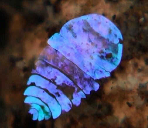
When waves travel through landscapes that contain disturbances, they naturally scatter, often in all directions. Scattering of light is a natural phenomenon, found in many places in nature. For example, the scattering of light is the reason for the blue color of the sky. As it turns out, when the length over which disturbances vary is much larger than the wavelength, the wave scatters in an unusual fashion: it forms channels (branches) of enhanced intensity that continue to divide or branch out, as the wave propagates.  This phenomenon is known as branched flow. It was first observed in 2001 in electrons and had been suggested to be ubiquitous and occur also for all waves in nature, for example – sound waves and even ocean waves. Now, Technion researchers are bringing branched flow to the domain of light: they have made an experimental observation of the branched flow of light.

“We always had the intention of finding something new, and we were eager to find it. It was not what we started looking for, but we kept looking and we found something far better,” says Asst. Prof. Miguel Bandres. “We are familiar with the fact that waves spread when they propagate in a homogeneous medium. But for other kinds of mediums, waves can behave in very different ways. When we have a disordered medium where the variations are not random but smooth, like a landscape of mountains and valleys, the waves will propagate in a peculiar way. They will form channels that keep dividing as the wave propagates, forming a beautiful pattern resembling the branches of a tree.” 

In their research, the team coupled a laser beam to a soap membrane, which contains random variations in membrane thickness. They discovered that when light propagates within the soap film, rather than being scattered, the light forms elongated branches, creating the branched flow phenomenon for light.

“In optics we usually work hard to make light stay focused and propagate as a collimated beam, but here the surprise is that the random structure of the soap film naturally caused the light to stay focused. It is another one of nature’s surprises,” says Tolik Patsyk. 

The ability to create branched flow in the field of optics offers new and exciting opportunities for investigating and understanding this universal wave phenomenon.

“There is nothing more exciting than discovering something new and this is the first demonstration of this phenomenon with light waves,” says Technion President Prof. Uri Sivan. “This goes to show that intriguing phenomena can also be observed in simple systems and one just has to be perceptive enough to uncover them. As such, bringing together and combining the views of researchers from different backgrounds and disciplines has led to some truly interesting insights.”

“The fact that we observe it with light waves opens remarkable new possibilities for research, starting with the fact that we can characterize the medium in which light propagates to very high precision and the fact that we can also follow those branches accurately and study their properties,” he adds.

Distinguished Prof. Moti Segev looks to the future. “I always educate my team to think beyond the horizon,” he says, “to think about something new, and at the same time – look at the experimental facts as they are, rather than try to adapt the experiments to meet some expected behavior. Here, Tolik was trying to measure something completely different and was surprised to see these light branches which he could not initially explain. He asked Miguel to join in the experiments, and together they upgraded the experiments considerably – to the level they could isolate the physics involved. That is when we started to understand what we see. It took more than a year until we understood that what we have is the strange phenomenon of “branched flow”, which at the time was never considered in the context of light waves. Now, with this observation – we can think of a plethora of new ideas. For example, using these light branches to control the fluidic flow in liquid, or to combine the soap with fluorescent material and cause the branches to become little lasers. Or to use the soap membranes as a platform for exploring fundamentals of waves, such as the transitions from ordinary scattering which is always diffusive, to branched flow, and subsequently to Anderson localization. There are many ways to continue this pioneering study. As we did many times in the past, we would like to boldly go where no one has gone before.” 

The project is now continuing in the laboratories of Profs. Segev and Sivan at Technion, and in parallel in the newly established lab of Prof. Miguel Bandres at UCF. 

Here’s a link to and a citation for the paper,

Observation of branched flow of light by Anatoly Patsyk, Uri Sivan, Mordechai Segev & Miguel A. Bandres Nature volume 583, pages60–65 (2020) DOI: https://doi.org/10.1038/s41586-020-2376-8 Published: 01 July 2020 Issue Date: 02 July 2020

This paper is behind a paywall.

Manipulating light at the nanoscale with kiragami-inspired technique

At left, different patterns of slices through a thin metal foil, are made by a focused ion beam. These patterns cause the metal to fold up into predetermined shapes, which can be used for such purposes as modifying a beam of light. Courtesy of the researchers

Nanokiragami (or nano-kiragami) is a fully fledged field of research? That was news to me as was much else in a July 6, 2018 news item on ScienceDaily,

Nanokirigami has taken off as a field of research in the last few years; the approach is based on the ancient arts of origami (making 3-D shapes by folding paper) and kirigami (which allows cutting as well as folding) but applied to flat materials at the nanoscale, measured in billionths of a meter.

Now, researchers at MIT [Massachusetts Institute of Technology] and in China have for the first time applied this approach to the creation of nanodevices to manipulate light, potentially opening up new possibilities for research and, ultimately, the creation of new light-based communications, detection, or computational devices.

A July 6, 2018 MIT news release (also on EurekAlert), which originated the news item, adds detail,

The findings are described today [July 6, 2018] in the journal Science Advances, in a paper by MIT professor of mechanical engineering Nicholas X Fang and five others. Using methods based on standard microchip manufacturing technology, Fang and his team used a focused ion beam to make a precise pattern of slits in a metal foil just a few tens of nanometers thick. The process causes the foil to bend and twist itself into a complex three-dimensional shape capable of selectively filtering out light with a particular polarization.

Previous attempts to create functional kirigami devices have used more complicated fabrication methods that require a series of folding steps and have been primarily aimed at mechanical rather than optical functions, Fang says. The new nanodevices, by contrast, can be formed in a single folding step and could be used to perform a number of different optical functions.

For these initial proof-of-concept devices, the team produced a nanomechanical equivalent of specialized dichroic filters that can filter out circularly polarized light that is either “right-handed” or “left-handed.” To do so, they created a pattern just a few hundred nanometers across in the thin metal foil; the result resembles pinwheel blades, with a twist in one direction that selects the corresponding twist of light.

The twisting and bending of the foil happens because of stresses introduced by the same ion beam that slices through the metal. When using ion beams with low dosages, many vacancies are created, and some of the ions end up lodged in the crystal lattice of the metal, pushing the lattice out of shape and creating strong stresses that induce the bending.

“We cut the material with an ion beam instead of scissors, by writing the focused ion beam across this metal sheet with a prescribed pattern,” Fang says. “So you end up with this metal ribbon that is wrinkling up” in the precisely planned pattern.

“It’s a very nice connection of the two fields, mechanics and optics,” Fang says. The team used helical patterns to separate out the clockwise and counterclockwise polarized portions of a light beam, which may represent “a brand new direction” for nanokirigami research, he says.

The technique is straightforward enough that, with the equations the team developed, researchers should now be able to calculate backward from a desired set of optical characteristics and produce the needed pattern of slits and folds to produce just that effect, Fang says.

“It allows a prediction based on optical functionalities” to create patterns that achieve the desired result, he adds. “Previously, people were always trying to cut by intuition” to create kirigami patterns for a particular desired outcome.

The research is still at an early stage, Fang points out, so more research will be needed on possible applications. But these devices are orders of magnitude smaller than conventional counterparts that perform the same optical functions, so these advances could lead to more complex optical chips for sensing, computation, or communications systems or biomedical devices, the team says.

For example, Fang says, devices to measure glucose levels often use measurements of light polarity, because glucose molecules exist in both right- and left-handed forms which interact differently with light. “When you pass light through the solution, you can see the concentration of one version of the molecule, as opposed to the mixture of both,” Fang explains, and this method could allow for much smaller, more efficient detectors.

Circular polarization is also a method used to allow multiple laser beams to travel through a fiber-optic cable without interfering with each other. “People have been looking for such a system for laser optical communications systems” to separate the beams in devices called optical isolaters, Fang says. “We have shown that it’s possible to make them in nanometer sizes.”

The team also included MIT graduate student Huifeng Du; Zhiguang Liu, Jiafang Li (project supervisor), and Ling Lu at the Chinese Academy of Sciences in Beijing; and Zhi-Yuan Li at the South China University of Technology. The work was supported by the National Key R&D Program of China, the National Natural Science Foundation of China, and the U.S Air Force Office of Scientific Research.

The researchers have also provided some GIFs,

And,

Here’s a link to and a citation for the paper,

Nano-kirigami with giant optical chirality by Zhiguang Liu, Huifeng Du, Jiafang Li, Ling Lu, Zhi-Yuan Li, and Nicholas X. Fang. Science Advances 06 Jul 2018: Vol. 4, no. 7, eaat4436 DOI: 10.1126/sciadv.aat4436

This paper is open access.

Art. Science. Optics. A Collider Café event in Vancouver (Canada) on January 23, 2019

The Curiosity Collider folks have decided to ring in the new year with an event focused on optics. Here’s more from their January 15, 2019 announcement (received via email),

FROM CONTEMPORARY ART TO SCIENCE ILLUSTRATION, IS “SEEING” REALLY
“BELIEVING”? OR IS THERE MORE TO IT THAN THERE SEEMS? HOW CAN WE EXPLORE
THE POSSIBILITIES THROUGH ART AND SCIENCE?

OUR #COLLIDERCAFE IS A SPACE FOR ARTISTS, SCIENTISTS, MAKERS, AND
ANYONE INTERESTED IN ART+SCIENCE. MEET, DISCOVER, CONNECT, CREATE. Are
you curious? Join us at “Collider Cafe: Art. Science. Optics.” to
explore how art and science intersect in the exploration of curiosity.

When: 8:00pm on Wednesday, January 23, 2019 Doors open at 7:30pm.
Where: Café Deux Soleils. 2096 Commercial Drive, Vancouver, BC (Google Map).
Cost: $5-10 (sliding scale) cover at the door. Proceeds will be used to cover the cost of running this event, and to fund future Curiosity Collider events.

With speakers:

Annie Briard, Contemporary Artist : What our eyes perceive but we do not see
Catherine Stewart, Visual Artist: The Museum as Muse: natural history collections as a resource for artistic exploration
Vicky Earle, Medical and Scientific Illustrator: The Art of Science & Medical Illustration
Ramey Newell, Photographer/Film Maker/Artist: Manifest Obscura: Reimagining/reimaging landscape through microbial collaboration
Julius T. Csotonyi, Paleoart, Natural History and Science Illustrator: A Mutualism of Endeavors

Head to the Facebook event page – let us know you are coming and share this event with others! Follow updates on instagram via @curiositycollider or #ColliderCafe. 

The announcement also includes other art/science events currently happening in Vancouver,

Looking for more Art+Science in Vancouver?

The work by one of our Collider Cafe speaker Catherine Stewart is on exhibition at the UBC Beaty Biodiversity Museum! “Skin & Bones” until August 13, 2019.

Another exhibition at the Beaty Biodiversity Museum: The Wild Creative by Asher Jay until April 28, 2019. “Examine biodiversity loss during the Anthropocene – the Age of Man – through compelling artworks and thought-provoking narratives.”

Our friends at the Story Collider will host their next Vancouver event “Kinship” on January 22. Learn more about the eventget tickets on Eventbrite.

Museum of Vancouver and Nature Vancouver are hosting Wild Things: The Power of Nature in Our Lives, an exhibition that delves into the life stories of local animals and plants. Interactive sessions every weekend. Until March 1, 2020.

For more Vancouver art+science events, visit the Curiosity Collider events calendar.

That last event (Wild Things at the Museum of Vancouver) is going to be available for viewing with a $5 Winter Wander ticket on February 2, 2019. A January 14, 2019 posting on the Miss604 blog has more,

Experience unique waterfront attractions showcasing art, history, crafts, science and performances during Winter Wander at Vanier Park on February 2, 2019. Enjoy local food vendors, enter to win great prizes, and get to know your local museum, space centre, archives, and more during this affordable, family-friendly event

Winter Wander at Vanier Park

When: Saturday, February 2, 2019 10:00am to 5:00pm
Venues include

Museum of Vancouver
The Museum of Vancouver inspires deeper understanding of the city through stories, objects and shared experiences. Check out their latest exhibits and their permanent collections and exhibition halls.

H.R. MacMillan Space Centre
The Space Centre is BC’s top space science attraction, inspiring visitors with shows, exhibits and some of Vancouver’s most unique special events

Vancouver Maritime Museum
Make some maritime-themed origami 10:00am to 4:30pm, visit with Parks Canada interpreters 10:00am to 4:30pm, climb on-board the St. Roch and celebrate 90 years of adventure, enjoy music from a string quartet onboard the St. Roch, and more

City of Vancouver Archives
The City Archives houses over 4 km of documents about the history of Vancouver, containing both government and public collections

Vancouver Academy of Music
Vancouver Academy of Music (“VAM”) is the city’s premiere centre of music education, serving aspiring musicians from early childhood to collegiate levels

Bonus: Bard on the Beach performances!

An undated posting at Vancouver’s Best Places gives you a sense of what to expect along with some handy tips,

At Winter Wander, expect lots of people, fair-sized lineups, and an event schedule with a list of entertainment and special activities throughout the day.

Live entertainment doesn’t happen all over the place. There is a set schedule and different things happen at specific times. The museums are open constantly all day. If you want to be entertained by the Bard on the Beach crew, however, you’ll need to check the schedule and be at a certain place at a certain time.

Although crowded, Winter Wander isn’t insanely busy. The venues are indeed crowded, but, surprisingly, not as bad as one might expect, or at least they weren’t when we’ve been. There is a pretty big lineup to get in before the doors even open in the morning, true, and you do need to wait your turn to get photos of your child in the model astronaut suit at the Planetarium, or to board the St. Roch police boat at the Maritime Museum.

Tips and Advic

Below are some tips and advice to help you make the most out of your experience at the Vanier Park museums on Winter Wander day

TIP #1: Go expecting the museums to be insanely crowded, and then hope to be pleasantly surprised. Go expecting small lineups and not too many people, however, and you’ll likely be disappointed

TIP #2: If you haven’t been to the museums at Vanier Park for a long time, you don’t mind crowds and you have children or guests from out of town, then definitely check out Winter Wander. For just $5, it’s a fabulous deal

TIP #3: Some venues and museum exhibit areas will be more popular and consequently more crowded than others. If a lineup for something is too long, simply move along to something else. There’s lots to see, so don’t fret if you don’t get to see everything

TIP #4: The best thing about the HR MacMillan Space Centre is the Planetarium and its shows about the stars and space. Chances are they’ll be busy, so don’t be disappointed if it’s not worth the wait. If you can get in to see a show though, do

TIP #5: Entertainment at Winter Wander happens at specific times and at certain places over the course of the day. When you arrive, check the schedule and decide what you want to see (including possible shows at the Planetarium). Then, plan your visit accordingly

TIP #6: Expect to spend between about an hour and all day at the event, but likely all morning or all afternoon. The length of your stay will depend on your level of interest in museums, model ships, history and space, but also on the crowds and the interest level and tolerance of crowds of the people you’re with

TIP #7: While at Vanier Park, go for a walk and explore. There is a beautiful walking trail all along the waterfront with views of the city. Especially if the museums are crowded, a break for some fresh air can be nice.

There you have it.

Constructing an autonomous Maxwell’s demon as a self-contained information-powered refrigerator

Aalto University (Finland) was the lead research institution for  INFERNOS, a European Union-funded project concerning Maxwell’s demon. Here’s an excerpt from an Oct. 14, 2013 post featuring the project,

An Oct. 9, 2013 news item on Nanowerk ties together INFERNOS and the ‘demon’,

Maxwell’s Demon is an imaginary creature that the mathematician James Clerk Maxwell created in 1897. The creature could turn heat into work without causing any other change, which violates the second law of thermodynamics. The primary goal of the European project INFERNOS (Information, fluctuations, and energy control in small systems) is to realize experimentally Maxwell’s Demon; in other words, to develop the electronic and biomolecular nanodevices that support this principle.

I like the INFERNOS logo, demon and all,

Logo of the European project INFERNOS (Information, fluctuations, and energy control in small systems).

A Jan. 11, 2016 news item on Nanowerk seems to be highlighting a paper resulting from the INFERNOS project (Note: A link has been removed),

On [a] theoretical level, the thought experiment has been an object of consideration for nearly 150 years, but testing it experimentally has been impossible until the last few years. Making use of nanotechnology, scientists from Aalto University have now succeeded in constructing an autonomous Maxwell’s demon that makes it possible to analyse the microscopic changes in thermodynamics. The research results were recently published in Physical Review Letters (“On-Chip Maxwell’s Demon as an Information-Powered Refrigerator”). The work is part of the forthcoming PhD thesis of MSc Jonne Koski at Aalto University.

An image illustrating the theory underlying the proposed device has been made available,

An autonomous Maxwell's demon. When the demon sees the electron enter the island (1.), it traps the electron with a positive charge (2.). When the electron leaves the island (3.), the demon switches back a negative charge (4.). Image: Jonne Koski.

An autonomous Maxwell’s demon. When the demon sees the electron enter the island (1.), it traps the electron with a positive charge (2.). When the electron leaves the island (3.), the demon switches back a negative charge (4.). Image: Jonne Koski.

A Jan. 11, 2016 Aalto University press release, which originated the news item, provides more technical details,

The system we constructed is a single-electron transistor that is formed by a small metallic island connected to two leads by tunnel junctions made of superconducting materials. The demon connected to the system is also a single-electron transistor that monitors the movement of electrons in the system. When an electron tunnels to the island, the demon traps it with a positive charge. Conversely, when an electron leaves the island, the demon repels it with a negative charge and forces it to move uphill contrary to its potential, which lowers the temperature of the system,’ explains Professor Jukka Pekola.

What makes the demon autonomous or self-contained is that it performs the measurement and feedback operation without outside help. Changes in temperature are indicative of correlation between the demon and the system, or, in simple terms, of how much the demon ‘knows’ about the system. According to Pekola, the research would not have been possible without the Low Temperature Laboratory conditions.

‘We work at extremely low temperatures, so the system is so well isolated that it is possible to register extremely small temperature changes,’ he says.

‘An electronic demon also enables a very large number of repetitions of the measurement and feedback operation in a very short time, whereas those who, elsewhere in the world, used molecules to construct their demons had to contend with not more than a few hundred repetitions.’

The work of the team led by Pekola remains, for the time being, basic research, but in the future, the results obtained may, among other things, pave the way towards reversible computing.

‘As we work with superconducting circuits, it is also possible for us to create qubits of quantum computers. Next, we would like to examine these same phenomena on the quantum level,’ Pekola reveals.

Here’s a link to and a citation for the paper,

On-Chip Maxwell’s Demon as an Information-Powered Refrigerator by J.V. Koski, A. Kutvonen, I.M. Khaymovich, T. Ala-Nissila, and J.P. Pekola. Phys. Rev. Lett. 115, 260602 DOI: http://dx.doi.org/10.1103/PhysRevLett.115.260602 Published 30 December 2015

This paper is behind a paywall.

One final comment, this is the 150th anniversary of Maxwell’s publication of a series of equations explaining the relationships between electric charges and electric and magnetic fields (featured here in a Nov. 27, 2015 posting).

The search for James Clerk Maxwell

The Brits really know how to celebrate an anniversary. In this case it’s the 150th anniversary of James Clerk Maxwell’s electromagnetic theory unifying electricity, magnetism, and light. (My Nov. 27, 2015 posting the first piece here featuring the anniversary and it describes the theory in more detail than you’ll find here.)

As part of the celebration there’s a five-episode series titled: Self Drives: Maxwell’s Equations being broadcast on BBC (British Broadcasting Corporation) 4. Stephen Curry writes about the series in a Dec. 9, 2015 posting on the Guardian science blogs (Note: Links have been removed),

There’s a potent antidote to the “Isn’t this amazing?” school of science communication and it’s called Will Self. In Self Drives: Maxwell’s Equations, which was broadcast recently [you can hear it as a podcast by visiting this site] on BBC Radio 4, the curious curmudgeon takes science to task once again as he goes in search of the mathematical and physical genius behind James Clerk Maxwell.

Over five short episodes, Self’s querulous quest takes him from Maxwell’s birthplace in Edinburgh to his family home in Glenlair, to the radio telescope at Jodrell Bank and the Diamond synchrotron near Oxford, and finally to Cambridge, where Maxwell studied mathematics in his youth and returned in his latter years as one of the nation’s most accomplished scientists to head the university’s Cavendish physics laboratory. Accompanying Self along the way is Akram Khan, the same physics professor who joined the errant writer on his earlier orbit of the Large Hadron Collider at CERN. I would have dubbed Khan Sancho Panza to Self’s Don Quixote but for this particular expedition the characters are reversed. It is Khan who wishes to see the poetry of science, while Self is happier to be grounded in prosaic and flawed reality. At CERN he refused truculently to worship in the cathedral of particle physics, stymied in equal measure by the difficulty of the subject matter and the boosterism of its scientific proponents. Here again the journey is mostly one of disappointment and frustration.

But not for the listener. The quest is far from fruitless, and nor is it lacking in emotional and intellectual force. Self’s documentary is not straight biography – you will find out more about Maxwell’s life and work from Wikipedia – but he has a different target in mind. …

Here’s the pair of explorers,

Will Self, Akram Khan and Maxwell’s infamous equations. Photograph: Laurence Grissell/BBC

Will Self, Akram Khan and Maxwell’s infamous equations. Photograph: Laurence Grissell/BBC

It’s good writing and an intriguing look into communicating science in a way that’s not quite so reverent and/or kid friendly as we tend to be in Canada.

James Clerk Maxwell and his science mashup unified theories of magnetism, electricity, and optics

It’s the 150th anniversary for a series of equations electric charges and electric and magnetic fields that are still being explored. Jon Butterworth in a Nov. 22, 2015 posting on the Guardian science blog network explains (Note: A link has been removed),

The chances are that you are reading this article on some kind of electronic technology. You are definitely seeing it via visible light, unless you have a braille or audio converter. And it probably got to you via wifi or a mobile phone signal. All of those things are understood in terms of the relationships between electric charges and electric and magnetic fields summarised in Maxwell’s [James Clerk Maxwell] equations, published by the Royal Society in 1865, 150 years ago.

Verbally, the equations can be summarised as something like:

Electric and magnetic fields make electric charges move. Electric charges cause electric fields, but there are no magnetic charges. Changes in magnetic fields cause electric fields, and vice versa.

The equations specify precisely how it all happens, but that is the gist of it.

Butterworth got a rare opportunity to see the original manuscript,

 Original manuscript of Maxwell’s seminal paper Photograph: Jon Butterworth/Royal Society [downloaded from http://www.theguardian.com/science/life-and-physics/2015/nov/22/maxwells-equations-150-years-of-light]

Original manuscript of Maxwell’s seminal paper Photograph: Jon Butterworth/Royal Society [downloaded from http://www.theguardian.com/science/life-and-physics/2015/nov/22/maxwells-equations-150-years-of-light]

I love this description from Butterworth,

It was submitted in 1864 but, in a situation familiar to scientists everywhere, was held up in peer review. There’s a letter, dated March 1865, from William Thomson (later Lord Kelvin) saying he was sorry for being slow, that he’d read most of it and it seemed pretty good (“decidely suitable for publication”).

Then, there’s this,

The equations seem to have been very much a bottom-up affair, in that Maxwell collected together a number of known laws which were used to describe various experimental results, and (with a little extra ingredient of his own) fitted them into a unified framework. What is amazing is how much that framework then reveals, both in terms of deep physical principles, and rich physical phenomena.

I’m not excerpting any part of Butterworth’s description of how Maxwell fit these equations together for his unification theory as I think it should be read in its totality.

The section on quantum mechanics is surprising,

Now, one thing Maxwell’s equations don’t contain is quantum mechanics [emphasis mine]. They are classical equations. But if you take the quantum mechnical description of an electron, and you enforce the same charge conservation law/voltage symmetry that was contained in the classical Maxwell’s equations, something marvellous happens [emphasis mine]. The symmetry is denoted “U(1)”, and if you enforce it locally – that it, you say that you have to be allowed make different U(1) type changes to electrons at different points in space, you actually generate the quantum mechanical version of Maxwell’s equations out of nowhere [emphasis mine]. You produce the equations that describe the photon, and the whole of quantum electrodynamics.

I encourage you to read Butterworth’s Nov. 22, 2015 posting where he also mention two related art/science projects and has embedded a video animation of the principles discussed in his posting.

For anyone unfamiliar with Butterworth, there’s this description at the Guardian,

Jon Butterworth is a physics professor at University College London. He is a member of the UCL High Energy Physics group and works on the Atlas experiment at Cern’s Large Hadron Collider. His book Smashing Physics: The Inside Story of the Hunt for the Higgs was published in May 2014

Nanocellulose as a biosensor

While nanocellulose always makes my antennae quiver (for anyone unfamiliar with the phrase, it means something along the lines of ‘attracts my attention’), it’s the collaboration which intrigues me most about this research. From a July 23, 2015 news item on Azonano (Note: A link has been removed),

An international team led by the ICREA Prof Arben Merkoçi has just developed new sensing platforms based on bacterial cellulose nanopaper. These novel platforms are simple, low cost and easy to produce and present outstanding properties that make them ideal for optical (bio)sensing applications. …

ICN2 [Catalan Institute of Nanoscience and Nanotechnology; Spain] researchers are going a step further in the development of simple, low cost and easy to produce biosensors. In an article published in ACS Nano they recently reported various innovative nanopaper-based optical sensing platforms. To achieve this endeavour the corresponding author ICREA Prof Arben Merkoçi, Group Leader at ICN2 and the first author, Dr Eden Morales-Narváez (from ICN2) and Hamed Golmohammadi (visiting researcher at ICN2), established an international collaboration with the Shahid Chamran University (Iran), the Gorgan University of Agricultural Sciences and Natural Resources (Iran) and the Academy of Sciences of the Czech Republic. [emphases mine]

Spain, Iran, and the Czech Republic. That’s an interesting combination of countries.

A July 23, 2015 ICN2 press release, which originated the news item, provides more explanations and detail,

Cellulose is simple, naturally abundant and low cost. However, cellulose fibres ranging at the nanoscale exhibit extraordinary properties such as flexibility, high crystallinity, biodegradability and optical transparency, among others. The nanomaterial can be extracted from plant cellulose pulp or synthetized by non-pathogenic bacteria. Currently, nanocellulose is under active research to develop a myriad of applications including filtration, wound dressing, pollution removal approaches or flexible and transparent electronics, whereas it has been scarcely explored for optical (bio)sensing applications.

The research team led by ICREA Prof Arben Merkoçi seeks to design, fabricate, and test simple, disposable and versatile sensing platforms based on this material. They designed different bacterial cellulose nanopaper based optical sensing platforms. In the article, the authors describe how the material can be tuned to exhibit plasmonic or photoluminescent properties that can be exploited for sensing applications. Specifically, they have prepared two types of plasmonic nanopaper and two types of photoluminescent nanopaper using different optically active nanomaterials.

The researchers took advantage of the optical transparency, porosity, hydrophilicity, and amenability to chemical modification of the material. The bacterial cellulose employed throughout this research was obtained using a bottom-up approach and it is shown that it can be easily turned into useful devices for sensing applications using wax printing or simple punch tools. The scientific team also demonstrates how these novel sensing platforms can be modulated to detect biologically relevant analytes such as cyanide and pathogens among others.

According to the authors, this class of platforms will prove valuable for displaying analytical information in diverse fields such as diagnostics, environmental monitoring and food safety. Moreover, since bacterial cellulose is flexible, lightweight, biocompatible and biodegradable, the proposed composites could be used as wearable optical sensors and could even be integrated into novel theranostic devices. In general, paper-based sensors are known to be simple, portable, disposable, low power-consuming and inexpensive devices that might be exploited in medicine, detection of explosives or hazardous compounds and environmental studies.

Here’s a link to and a citation for the paper,

Nanopaper as an Optical Sensing Platform by Eden Morales-Narváez, Hamed Golmohammadi, Tina Naghdi, Hossein Yousefi, Uliana Kostiv, Daniel Horák, Nahid Pourreza, and Arben Merkoçi.ACS Nano, Article ASAP DOI: 10.1021/acsnano.5b03097 Publication Date (Web): July 2, 2015
Copyright © 2015 American Chemical Society

This paper is behind a paywall.

Sea sapphires: now you see them, now you don’t and more about structural colour/color

The structural colour of the sea sapphire

 Scientists are studying the disappearing act of this ocean-dwelling copepod. Credit: Kaj Maney, www.liquidguru.com Courtesy: American Chemical Society


Scientists are studying the disappearing act of this ocean-dwelling copepod.
Credit: Kaj Maney, www.liquidguru.com Courtesy: American Chemical Society

Now, you’ve seen a sea sapphire. Here’s more about them and the interest they hold for experts in photonics, from a July 15, 2015 news item on ScienceDaily,

Sapphirina, or sea sapphire, has been called “the most beautiful animal you’ve never seen,” and it could be one of the most magical. Some of the tiny, little-known copepods appear to flash in and out of brilliantly colored blue, violet or red existence. Now scientists are figuring out the trick to their hues and their invisibility. The findings appear in the Journal of the American Chemical Society and could inspire the next generation of optical technologies.

A July 15, 2015 American Chemical Society (ACS) news release, which originated the news item, provides more detail,

Copepods are tiny aquatic crustaceans that live in both fresh and salt water. Some males of the ocean-dwelling Sapphirina genus display striking, iridescent colors that scientists think play a role in communication and mate recognition. The shimmering animals’ colors result when light bounces off of the thin, hexagonal crystal plates that cover their backs. These plates also help them vanish, if only fleetingly. Scientists didn’t know specifically what factors contributed to creating different shades. Scientists at the Weizmann Institute [Israel] and the Interuniversity Institute for Marine Sciences in Eilat [Israel] wanted to investigate the matter.

The researchers measured the light reflectance — which determines color — of live Sapphirina males and the spacing between crystal layers. They found that changes of reflectance depended on the thickness of the spacing. And for at least one particular species, when light hits an animal at a 45-degree angle, reflectance shifts out of the visible light range and into the ultraviolet, and it practically disappears. Their results could help inform the design of artificial photonic crystal structures, which have many potential uses in reflective coatings, optical mirrors and optical displays.

To sum this up, the colour and the invisibility properties are due to thin, hexagonal crystal plates and the spacing of these plates, in other words, structural colour, which is usually achieved at the nanoscale.

Here’s a link to and a citation for the paper,

Structural Basis for the Brilliant Colors of the Sapphirinid Copepods by Dvir Gur, Ben Leshem, Maria Pierantoni, Viviana Farstey, Dan Oron, Steve Weiner, and Lia Addadi. J. Am. Chem. Soc., 2015, 137 (26), pp 8408–8411 DOI: 10.1021/jacs.5b05289 Publication Date (Web): June 22, 2015

Copyright © 2015 American Chemical Society

This paper is behind a paywall.

For anyone who’s interested, Lynn Kimlicka has a nice explanation of structural colour in a July 22, 2015 posting on the Something About Science blog where she discusses some recent research iridescence in bird feathers and synthetic melanin. She also shares a picture of her budgie and its iridescent feathers. The ‘melanin’ research was mentioned here in a May 19, 2015 posting where I also provide a link to a great 2013 piece on structural throughout the animal and plant kingdoms by Cristina Luiggi for The Scientist.

Understanding how nanostructures can affect optical properties could be leading to new ways of managing light. A July 23, 2015 news item on ScienceDaily describes a project at the University of Delaware dedicated to “changing the color of light,”

Researchers at the University of Delaware have received a $1 million grant from the W.M. Keck Foundation to explore a new idea that could improve solar cells, medical imaging and even cancer treatments. Simply put, they want to change the color of light.

A July 23, 2015 University of Delaware (UD) news release, which originated the news item, provides more information about the proposed research,

“A ray of light contains millions and millions of individual units of light called photons,” says project leader Matthew Doty. “The energy of each photon is directly related to the color of the light — a photon of red light has less energy than a photon of blue light. You can’t simply turn a red photon into a blue one, but you can combine the energy from two or more red photons to make one blue photon.”

This process, called “photon upconversion,” isn’t new, Doty says. However, the UD team’s approach to it is.

They want to design a new kind of semiconductor nanostructure that will act like a ratchet. It will absorb two red photons, one after the other, to push an electron into an excited state when it can emit a single high-energy (blue) photon.

These nanostructures will be so teeny they can only be viewed when magnified a million times under a high-powered electron microscope.

“Think of the electrons in this structure as if they were at a water park,” Doty says. “The first red photon has only enough energy to push an electron half-way up the ladder of the water slide. The second red photon pushes it the rest of the way up. Then the electron goes down the slide, releasing all of that energy in a single process, with the emission of the blue photon. The trick is to make sure the electron doesn’t slip down the ladder before the second photon arrives. The semiconductor ratchet structure is how we trap the electron in the middle of the ladder until the second photon arrives to push it the rest of the way up.”

The UD team will develop new semiconductor structures containing multiple layers of different materials, such as aluminum arsenide and gallium bismuth arsenide, each only a few nanometers thick. This “tailored landscape” will control the flow of electrons into states with varying potential energy, turning once-wasted photons into useful energy.

The UD team has shown theoretically that their semiconductors could reach an upconversion efficiency of 86 percent, which would be a vast improvement over the 36 percent efficiency demonstrated by today’s best materials. What’s more, Doty says, the amount of light absorbed and energy emitted by the structures could be customized for a variety of applications, from lightbulbs to laser-guided surgery.

How do you even begin to make structures so tiny they can only be seen with an electron microscope? In one technique the UD team will use, called molecular beam epitaxy, nanostructures will be built by depositing layers of atoms one at a time. Each structure will be tested to see how well it absorbs and emits light, and the results will be used to tailor the structure to improve performance.

The researchers also will develop a milk-like solution filled with millions of identical individual nanoparticles, each one containing multiple layers of different materials. The multiple layers of this structure, like multiple candy shells in an M&M, will implement the photon ratchet idea. Through such work, the team envisions a future upconversion “paint” that could be easily applied to solar cells, windows and other commercial products.

Improving medical tests and treatments

While the initial focus of the three-year project will be on improving solar energy harvesting, the team also will explore biomedical applications.

A number of diagnostic tests and medical treatments, ranging from CT [computed tomography] and PET [positron emission tomography] scans to chemotherapy, rely on the release of fluorescent dyes and pharmaceutical drugs. Ideally, such payloads are delivered both at specific disease sites and at specific times, but this is hard to control in practice.

The UD team aims to develop an upconversion nanoparticle that can be triggered by light to release its payload. The goal is to achieve the controlled release of drug therapies even deep within diseased human tissue while reducing the peripheral damage to normal tissue by minimizing the laser power required.

“This is high-risk, high-reward research,” Doty says. “High-risk because we don’t yet have proof-of-concept data. High-reward because it has such a huge potential impact in renewable energy to medicine. It’s amazing to think that this same technology could be used to harvest more solar energy and to treat cancer. We’re excited to get started!”

That’s it for structural colour/color today.

Nanoscale device emits light as powerfully as an object 10,000 times its size

The potential application in the field of solar power is what most interests me in this collaborative research from the University of Wisconsin-Madison (US) and Fudan University in China. From a July 13, 2015 news item on ScienceDaily,

University of Wisconsin-Madison engineers have created a nanoscale device that can emit light as powerfully as an object 10,000 times its size. It’s an advance that could have huge implications for everything from photography to solar power.

In a paper published July 10 [2015] in the journal Physical Review Letters, Zongfu Yu, an assistant professor of electrical and computer engineering, and his collaborators describe a nanoscale device that drastically surpasses previous technology in its ability to scatter light. They showed how a single nanoresonator can manipulate light to cast a very large “reflection.” The nanoresonator’s capacity to absorb and emit light energy is such that it can make itself — and, in applications, other very small things — appear 10,000 times as large as its physical size.

A July 13, 2015 University of Wisconsin-Madison news release (also on EurekAlert) by Scott Gordon, which originated the news item, expands on the theme,

“Making an object look 10,000 times larger than its physical size has lots of implications in technologies related to light,” Yu says.

The researchers realized the advance through materials innovation and a keen understanding of the physics of light. Much like sound, light can resonate, amplifying itself as the surrounding environment manipulates the physical properties of its wave energy. The researchers took advantage of this by creating an artificial material in which the wavelength of light is much larger than in a vacuum, which allows light waves to resonate more powerfully.

The device condenses light to a size smaller than its wavelength, meaning it can gather a lot of light energy, and then scatters the light over a very large area, harnessing its output for imaging applications that make microscopic particles appear huge.

“The device makes an object super-visible by enlarging its optical appearance with this super-strong scattering effect,” says Ming Zhou, a Ph.D. student in Yu’s group and lead author of the paper.

Much as a very thin string on a guitar can absorb a large amount of acoustic energy from its surroundings and begin to vibrate in sympathy, this one very small optical device can receive light energy from all around and yield a surprisingly strong output. In imaging, this presents clear advantages over conventional lenses, whose light-gathering capacity is limited by direction and size.

“We are developing photodetectors based on this technology and, for example, it could be helpful for photographers wanting to shoot better quality pictures in weak light conditions,” Yu says.

Given the nanoresonator’s capacity to absorb large amounts of light energy, the technology also has potential in applications that harvest the sun’s energy with high efficiency. In addition, Yu envisions simply letting the resonator emit that energy in the form of infrared light toward the sky, which is very cold. Because the nanoresonator has a large optical cross-section — that is, an ability to emit light that dramatically exceeds its physical size — it can shed a lot of heat energy, making for a passive cooling system.

“This research opens up a new way to manipulate the flow of light, and could enable new technologies in light sensing and solar energy conversion,” Yu says.

Here’s a link to and a citation for the paper,

Extraordinarily Large Optical Cross Section for Localized Single Nanoresonator by Ming Zhou, Lei Shi, Jian Zi, and Zongfu Yu. Phys. Rev. Lett. 115, 023903  DOI: http://dx.doi.org/10.1103/PhysRevLett.115.023903 Published 10 July 2015

This paper is behind a paywall.

Chameleon-like artificial skin

A March 12, 2015 news item on phys.org describes artificial skin inspired by chameleons,

Borrowing a trick from nature, engineers from the University of California at Berkeley have created an incredibly thin, chameleon-like material that can be made to change color—on demand—by simply applying a minute amount of force.

This new material-of-many-colors offers intriguing possibilities for an entirely new class of display technologies, color-shifting camouflage, and sensors that can detect otherwise imperceptible defects in buildings, bridges, and aircraft.

“This is the first time anybody has made a flexible chameleon-like skin that can change color simply by flexing it,” said Connie J. Chang-Hasnain, a member of the Berkeley team and co-author on a paper published today in Optica, The Optical Society’s (OSA) new journal.

A March 12, 2015 OSA news release (also on EurekAlert), which originated the news item, provides more information about this structural color project,

The colors we typically see in paints, fabrics, and other natural substances occur when white, broad spectrum light strikes their surfaces. The unique chemical composition of each surface then absorbs various bands, or wavelengths of light. Those that aren’t absorbed are reflected back, with shorter wavelengths giving objects a blue hue and longer wavelengths appearing redder and the entire rainbow of possible combinations in between. Changing the color of a surface, such as the leaves on the trees in autumn, requires a change in chemical make-up.

Recently, engineers and scientists have been exploring another approach, one that would create designer colors without the use of chemical dyes and pigments. Rather than controlling the chemical composition of a material, it’s possible to control the surface features on the tiniest of scales so they interact and reflect particular wavelengths of light. This type of “structural color” is much less common in nature, but is used by some butterflies and beetles to create a particularly iridescent display of color.

Controlling light with structures rather than traditional optics is not new. In astronomy, for example, evenly spaced slits known as diffraction gratings are routinely used to direct light and spread it into its component colors. Efforts to control color with this technique, however, have proved impractical because the optical losses are simply too great.

The authors of the Optica paper applied a similar principle, though with a radically different design, to achieve the color control they were looking for. In place of slits cut into a film they instead etched rows of ridges onto a single, thin layer of silicon. Rather than spreading the light into a complete rainbow, however, these ridges — or bars — reflect a very specific wavelength of light. By “tuning” the spaces between the bars, it’s possible to select the specific color to be reflected. Unlike the slits in a diffraction grating, however, the silicon bars were extremely efficient and readily reflected the frequency of light they were tuned to.

Fascinatingly, the reflected colors can be selected (from the news release),

Since the spacing, or period, of the bars is the key to controlling the color they reflect, the researchers realized it would be possible to subtly shift the period — and therefore the color — by flexing or bending the material.

“If you have a surface with very precise structures, spaced so they can interact with a specific wavelength of light, you can change its properties and how it interacts with light by changing its dimensions,” said Chang-Hasnain.

Earlier efforts to develop a flexible, color shifting surface fell short on a number of fronts. Metallic surfaces, which are easy to etch, were inefficient, reflecting only a portion of the light they received. Other surfaces were too thick, limiting their applications, or too rigid, preventing them from being flexed with sufficient control.

The Berkeley researchers were able to overcome both these hurdles by forming their grating bars using a semiconductor layer of silicon approximately 120 nanometers thick. Its flexibility was imparted by embedding the silicon bars into a flexible layer of silicone. As the silicone was bent or flexed, the period of the grating spacings responded in kind.

The semiconductor material also allowed the team to create a skin that was incredibly thin, perfectly flat, and easy to manufacture with the desired surface properties. This produces materials that reflect precise and very pure colors and that are highly efficient, reflecting up to 83 percent of the incoming light.

Their initial design, subjected to a change in period of a mere 25 nanometers, created brilliant colors that could be shifted from green to yellow, orange, and red – across a 39-nanometer range of wavelengths. Future designs, the researchers believe, could cover a wider range of colors and reflect light with even greater efficiency.

Here’s a link to and a citation for the paper,

Flexible photonic metastructures for tunable coloration by Li Zhu, Jonas Kapraun, James Ferrara, and Connie J. Chang-Hasnain. Optica, Vol. 2, Issue 3, pp. 255-258 (2015)
http://dx.doi.org/10.1364/OPTICA.2.000255

This paper is open access (for now at least).

Final note: I recently wrote about research into how real chameleons are able to effect colour changes in a March 16, 2015 post.