Category Archives: electronics

Growing electrodes in your brain?

This isn’t for everybody. From a February 23, 2023 news item on Nanowerk, Note: A link has been removed,

The boundaries between biology and technology are becoming blurred. Researchers at Linköping, Lund, and Gothenburg universities in Sweden have successfully grown electrodes in living tissue using the body’s molecules as triggers. The result, published in the journal Science (“Metabolite-induced in vivo fabrication of substrate-free organic bioelectronics”), paves the way for the formation of fully integrated electronic circuits in living organisms.
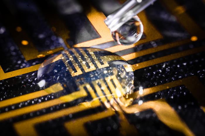
Caption: The injectable gel being tested on a microfabricated circuit. Credit: Thor Balkhed

I have two news releases for this research. First, the February 23, 2023 American Association for the Advancement of Science (AAAS) news release on EurekAlert,

Researchers have developed a way to make bioelectronics directly inside living tissues, an approach they tested by making electrodes in the brain, heart, and fin tissue of living zebrafish, as well as in isolated mammalian muscle tissues. According to the authors, the new method paves the way for in vivo fabrication of fully integrated electronic circuits within the nervous system and other living tissue. “Safety and stability analyses over long periods will be essential to determining whether such technology is useful for chronic implantations,” writes Sahika Inal in a related Perspective. “However, the strategy … suggests that any living tissue can turn into electronic matter and brings the field closer to generating seamless biotic-abiotic interfaces with a potentially long lifetime and minimum harm to tissues.” Implantable electronic devices that can interface with soft biological neural tissues offer a valuable approach to studying the complex electrical signaling of the nervous system and enable the therapeutic modulation of neural circuitry to prevent or treat various diseases and disorders. However, conventional bioelectronic implants often require the use of rigid electronic substrates that are incompatible with delicate living tissues and can provoke injury and inflammation that can affect a device’s electrical properties and long-term performance. Overcoming the incompatibility between static, solid-state electronic materials and dynamic, soft biological tissues has proven challenging. Here, Xenofon Strakosas and colleagues present a method to fabricate polymer-based, substrate-free electronic conducting materials directly inside a tissue. Strakosas et al. developed a complex molecular precursor cocktail that, when injected into a tissue, uses endogenous metabolites (glucose and lactate) to induce polymerization of organic precursors to form conducting polymer gels. To demonstrate the approach, the authors “grew” gel electrodes in the brain, heart, and fin tissue of living zebrafish, with no signs of tissue damage, and in isolated mammalian muscle tissues, including beef, pork and chicken. In medicinal leeches, they showed how the conducting gel could interface nervous tissue with electrodes on a tiny flexible probe.

The second is the February 23, 2023 Linköping University press release on EurekAlert, which originated the news item, and it provides further insight,

“For several decades, we have tried to create electronics that mimic biology. Now we let biology create the electronics for us,” says Professor Magnus Berggren at the Laboratory for Organic Electronics, LOE, at Linköping University.

Linking electronics to biological tissue is important to understand complex biological functions, combat diseases in the brain, and develop future interfaces between man and machine. However, conventional bioelectronics, developed in parallel with the semiconductor industry, have a fixed and static design that is difficult, if not impossible, to combine with living biological signal systems.

To bridge this gap between biology and technology, researchers have developed a method for creating soft, substrate-free, electronically conductive materials in living tissue. By injecting a gel containing enzymes as the “assembly molecules”, the researchers were able to grow electrodes in the tissue of zebrafish and medicinal leeches.

“Contact with the body’s substances changes the structure of the gel and makes it electrically conductive, which it isn’t before injection. Depending on the tissue, we can also adjust the composition of the gel to get the electrical process going,” says Xenofon Strakosas, researcher at LOE and Lund University and one of the study’s main authors.

The body’s endogenous molecules are enough to trigger the formation of electrodes. There is no need for genetic modification or external signals, such as light or electrical energy, which has been necessary in previous experiments. The Swedish researchers are the first in the world to succeed in this.

Their study paves the way for a new paradigm in bioelectronics. Where it previously took implanted physical objects to start electronic processes in the body, injection of a viscous gel will be enough in the future.

In their study, the researchers further show that the method can target the electronically conducting material to specific biological substructures and thereby create suitable interfaces for nerve stimulation. In the long term, the fabrication of fully integrated electronic circuits in living organisms may be possible.

In experiments conducted at Lund University, the team successfully achieved electrode formation in the brain, heart, and tail fins of zebrafish and around the nervous tissue of medicinal leeches. The animals were not harmed by the injected gel and were otherwise not affected by the electrode formation. One of the many challenges in these trials was to take the animals’ immune system into account.

“By making smart changes to the chemistry, we were able to develop electrodes that were accepted by the brain tissue and immune system. The zebrafish is an excellent model for the study of organic electrodes in brains,” says Professor Roger Olsson at the Medical Faculty at Lund University, who also has a chemistry laboratory at the University of Gothenburg.

It was Professor Roger Olsson who took the initiative for the study, after he read about the electronic rose developed by researchers at Linköping University in 2015. One research problem, and an important difference between plants and animals, was the difference in cell structure. Whereas plants have rigid cell walls which allow for the formation of electrodes, animal cells are more like a soft mass. Creating a gel with enough structure and the right combination of substances to form electrodes in such surroundings was a challenge that took many years to solve.

“Our results open up for completely new ways of thinking about biology and electronics. We still have a range of problems to solve, but this study is a good starting point for future research,” says Hanne Biesmans, PhD student at LOE and one of the main authors.

Here’s a link to and a citation for the paper,

Metabolite-induced in vivo fabrication of substrate-free organic bioelectronics by Xenofon Strakosas, Hanne Biesmans, Tobias Abrahamsson, Karin Hellman, Malin Silverå Ejneby, Mary J. Donahue, Peter Ekström, Fredrik Ek, Marios Savvakis, Martin Hjort, David Bliman, Mathieu Linares, Caroline Lindholm, Eleni Stavrinidou, Jennifer Y. Gerasimov, Daniel T. Simon, Roger Olsson, and Magnus Berggren. Science 23 Feb 2023 Vol 379, Issue 6634 pp. 795-802 DOI: 10.1126/science.adc9998

This paper is behind a paywall.
A jellybean solution to a problem with quantum computing chips

https://youtube.com/watch?v=BDeNF0IRfvE

A May 11, 2023 news item on phys.org heralds this new development, Note: A link has been removed,

The silicon microchips of future quantum computers will be packed with millions, if not billions of qubits—the basic units of quantum information—to solve the greatest problems facing humanity. And with millions of qubits needing millions of wires in the microchip circuitry, it was always going to get cramped in there.

But now engineers at UNSW [University of New South Wales] Sydney have made an important step toward solving a long-standing problem about giving their qubits more breathing space—and it all revolves around jellybeans.

Not the kind we rely on for a sugar hit to get us past the 3pm slump. But jellybean quantum dots –elongated areas between qubit pairs that create more space for wiring without interrupting the way the paired qubits interact with each other.

A May 10, 2023 University of New South Wales (UNSW) press release (also published on EurekAlert), which originated the news item, delves further into the ‘jellbean solution’, Note: A link has been removed,

As lead author Associate Professor Arne Laucht explains, the jellybean quantum dot is not a new concept in quantum computing, and has been discussed as a solution to some of the many pathways towards building the world’s first working quantum computer.

“It has been shown in different material systems such as gallium arsenide. But it has not been shown in silicon before,” he says.

Silicon is arguably one of the most important materials in quantum computing, A/Prof. Laucht says, as the infrastructure to produce future quantum computing chips is already available, given we use silicon chips in classical computers. Another benefit is that you can fit so many qubits (in the form of electrons) on the one chip.

“But because the qubits need to be so close together to share information with one another, placing wires between each pair was always going to be a challenge.”

In a study published today in Advanced Materials, the UNSW team of engineers describe how they showed in the lab that jellybean quantum dots were possible in silicon. This now opens the way for qubits to be spaced apart to ensure that the wires necessary to connect and control the qubits can be fit in between.

How it works

In a normal quantum dot using spin qubits, single electrons are pulled from a pool of electrons in silicon to sit under a ‘quantum gate’ – where the spin of each electron represents the computational state. For example, spin up may represent a 0 and spin down could represent a 1. Each qubit can then be controlled by an oscillating magnetic field of microwave frequency.

But to implement a quantum algorithm, we also need two-qubit gates, where the control of one qubit is conditional on the state of the other. For this to work, both quantum dots need to be placed very closely, just a few 10s of nanometres apart so their spins can interact with one another. (To put this in perspective, a single human hair is about 100,000 nanometres thick.)

But moving them further apart to create more real estate for wiring has always been the challenge facing scientists and engineers. The problem was as the paired qubits move apart, they would then stop interacting.

The jellybean solution represents a way of having both: nicely spaced qubits that continue to influence one another. To make the jellybean, the engineers found a way to create a chain of electrons by trapping more electrons in between the qubits. This acts as the quantum version of a string phone so that the two paired qubit electrons at each end of the jellybean can continue to talk to another. Only the electrons at each end are involved in any computations, while the electrons in the jellybean dot are there to keep them interacting while spread apart.

The lead author of the paper, former PhD student Zeheng Wang says the number of extra electrons pulled into the jellybean quantum dot is key to how they arrange themselves.

“We showed in the paper that if you only load a few electrons in that puddle of electrons that you have underneath, they break into smaller puddles. So it’s not one continuous jellybean quantum dot, it’s a smaller one here, and a bigger one in the middle and a smaller one there. We’re talking of a total of three to maybe ten electrons.

“It’s only when you go to larger numbers of electrons, say 15 or 20 electrons, that the jellybean becomes more continuous and homogeneous. And that’s where you have your well-defined spin and quantum states that you can use to couple qubits to another.”

Post-jellybean quantum world

A/Prof. Laucht stresses that there is still much work to be done. The team’s efforts for this paper focused on proving the jellybean quantum dot is possible. The next step is to insert working qubits at each end of the jellybean quantum dot and make them talk to another.

“It is great to see this work realised. It boosts our confidence that jellybean couplers can be utilised in silicon quantum computers, and we are excited to try implementing them with qubits next.”

Whoever wrote the press release seems to have had a lot of fun with the jellybeans. Thank you.

Here’s a link to and a citation for the paper,

Jellybean Quantum Dots in Silicon for Qubit Coupling and On-Chip Quantum Chemistry by Zeheng Wang, MengKe Feng, Santiago Serrano, William Gilbert, Ross C. C. Leon, Tuomo Tanttu, Philip Mai, Dylan Liang, Jonathan Y. Huang, Yue Su, Wee Han Lim, Fay E. Hudson,  Christopher C. Escott, Andrea Morello, Chih Hwan Yang, Andrew S. Dzurak, Andre Saraiva, Arne Laucht. Advanced Materials Volume 35, Issue 19 May 11, 2023 2208557 DOI: https://doi.org/10.1002/adma.202208557 First published online: 20 February 2023

This paper is open access.

Sound waves for wearable patches that deliver drugs painlessly

While watching this video I started wondering if they were testing their research on students but that’s not the case; these wearable patches were tested on porcine (pig) skin, which is quite similar to human skin, Note: They tested a B vitamin called niacinamide so, it’s highly unlikely the pigs suffered from it,

An April 20, 2023 news item on ScienceDaily announces the research into using ultrasonic waves for drug delivery,

The skin is an appealing route for drug delivery because it allows drugs to go directly to the site where they’re needed, which could be useful for wound healing, pain relief, or other medical and cosmetic applications. However, delivering drugs through the skin is difficult because the tough outer layer of the skin prevents most small molecules from passing through it.

In hopes of making it easier to deliver drugs through the skin, MIT [Massachusetts Institute of Technology] researchers have developed a wearable patch that applies painless ultrasonic waves to the skin, creating tiny channels that drugs can pass through. This approach could lend itself to delivery of treatments for a variety of skin conditions, and could also be adapted to deliver hormones, muscle relaxants, and other drugs, the researchers say.

An April 20, 2023 Massachusetts Institute of Technology (MIT) news release (also on EurekAlert), which originated the news item, provides technical details about the research, Note: A link has been removed,

“The ease-of-use and high-repeatability offered by this system provides a game-changing alternative to patients and consumers suffering from skin conditions and premature skin aging,” says Canan Dagdeviren, an associate professor in MIT’s Media Lab and the senior author of the study. “Delivering drugs this way could offer less systemic toxicity and is more local, comfortable, and controllable.”

MIT research assistants Chia-Chen Yu and Aastha Shah are the lead authors of the paper, which appears in Advanced Materials, as part of the journal’s “Rising Stars” series, which showcases the outstanding work of researchers in the early stages of their independent careers. Other MIT authors include Research Assistant Colin Marcus and postdoc Md Osman Goni Nayeem. Nikta Amiri, Amit Kumar Bhayadia, and Amin Karami of the University of Buffalo are also authors of the paper.

A boost from sound waves

The researchers began this project as an exploration of alternative ways to deliver drugs. Most drugs are delivered orally or intravenously, but the skin is a route that could offer much more targeted drug delivery for certain applications.

“The main benefit with skin is that you bypass the whole gastrointestinal tract. With oral delivery, you have to deliver a much larger dose in order to account for the loss that you would have in the gastric system,” Shah says. “This is a much more targeted, focused modality of drug delivery.”

Ultrasound exposure has been shown to enhance the skin’s permeability to small-molecule drugs, but most of the existing techniques for performing this kind of drug delivery require bulky equipment. The MIT team wanted to come up with a way to perform this kind of transdermal drug delivery with a lightweight, wearable patch, which could make it easier to use for a variety of applications.

The device that they designed consists of a patch embedded with several disc-shaped piezoelectric transducers, which can convert electric currents into mechanical energy. Each disc is embedded in a polymeric cavity that contains the drug molecules dissolved in a liquid solution. When an electric current is applied to the piezoelectric elements, they generate pressure waves in the fluid, creating bubbles that burst against the skin. These bursting bubbles produce microjets of fluid that can penetrate through the skin’s tough outer layer, the stratum corneum.

“This works open the door to using vibrations to enhance drug delivery. There are several parameters that result in generation of different kinds of waveform patterns. Both mechanical and biological aspects of drug delivery can be improved by this new toolset,” Karami says.

The patch is made of PDMS, a silicone-based polymer that can adhere to the skin without tape. In this study, the researchers tested the device by delivering a B vitamin called niacinamide, an ingredient in many sunscreens and moisturizers.

In tests using pig skin, the researchers showed that when they delivered niacinamide using the ultrasound patch, the amount of drug that penetrated the skin was 26 times greater than the amount that could pass through the skin without ultrasonic assistance.

The researchers also compared the results from their new device to microneedling, a technique sometimes used for transdermal drug delivery, which involves puncturing the skin with miniature needles. The researchers found that their patch was able to deliver the same amount of niacinamide in 30 minutes that could be delivered with microneedles over a six-hour period.

Local delivery

With the current version of the device, drugs can penetrate a few millimeters into the skin, making this approach potentially useful for drugs that act locally within the skin. These could include niacinamide or vitamin C, which is used to treat age spots or other dark spots on the skin, or topical drugs used to heal burns.

With further modifications to increase the penetration depth, this technique could also be used for drugs that need to reach the bloodstream, such as caffeine, fentanyl, or lidocaine. Dagdeviren also envisions that this kind of patch could be useful for delivering hormones such as progesterone. In addition, the researchers are now exploring the possibility of implanting similar devices inside the body to deliver drugs to treat cancer or other diseases.

The researchers are also working on further optimizing the wearable patch, in hopes of testing it soon on human volunteers. They also plan to repeat the lab experiments they did in this study, with larger drug molecules.

“After we characterize the drug penetration profiles for much larger drugs, we would then see which candidates, like hormones or insulin, can be delivered using this technology, to provide a painless alternative for those who are currently bound to self-administer injections on a daily basis,” Shah says.

Here’s a link to and a citation for the paper,

A Conformable Ultrasound Patch for Cavitation-Enhanced Transdermal Cosmeceutical Delivery by Chia-Chen Yu, Aastha Shah, Nikta Amiri, Colin Marcus, Md Osman Goni Nayeem, Amit Kumar Bhayadia, Amin Karami, Canan Dagdeviren. Advanced Materials Volume35, Issue 23 June 8, 2023 2300066 DOI: https://doi.org/10.1002/adma.202300066 First published online: 19 March 2023

This paper is open access.

Biobattery with a 100-year shelf life

According to an April 18, 2023 news item on ScienceDaily this long-lasting (100 years potentially) biobattery runs on bacteria,

A tiny biobattery that could still work after 100 years has been developed by researchers at Binghamton University, State University of New York.

Last fall [2022], Binghamton University Professor Seokheun “Sean” Choi and his Bioelectronics and Microsystems Laboratory published their research into an ingestible biobattery activated by the Ph factor of the human intestine.

Now, he and PhD student Maryam Rezaie have taken what they learned and incorporated it into new ideas for use outside the body.

A new study in the journal Small, which covers nanotechnology, shares the results from using spore-forming bacteria similar to the previous ingestible version to create a device that potentially would still work after 100 years.

An April 12, 2023 Binghamton University news release (also on EurekAlert but published April 18, 2023) by Chris Kocher, which originated the news item, highlights the researcher’s perspective on this work,

“The overall objective is to develop a microbial fuel cell that can be stored for a relatively long period without degradation of biocatalytic activity and also can be rapidly activated by absorbing moisture from the air,” said Choi, a faculty member in the Department of Electrical and Computer Engineering at the Thomas J. Watson College of Engineering and Applied Science.

“We wanted to make these biobatteries for portable, storable and on-demand power generation capabilities,” Choi said. “The problem is, how can we provide the long-term storage of bacteria until used? And if that is possible, then how would you provide on-demand battery activation for rapid and easy power generation? And how would you improve the power?”

The dime-sized fuel cell was sealed with a piece of Kapton tape, a material that can withstand temperatures from -500 to 750 degrees Fahrenheit. When the tape was removed and moisture allowed in, the bacteria mixed with a chemical germinant that encouraged the microbes to produce spores. The energy from that reaction produced enough to power an LED, a digital thermometer or a small clock.

Heat activation of the bacterial spores cut the time to full power from 1 hour to 20 minutes, and increasing the humidity led to higher electrical output. After a week of storage at room temperature, there was only a 2% drop in power generation.

The study is funded by the [US] Office of Naval Research, and it’s easy to imagine the military applications for a power source that could be deployed on the battlefield or in remote locations. However, there would be plenty of civilian uses for such a fuel cell, too.

While these are all good results, Choi knows that a fuel cell like this needs to power up more quickly and produce more voltage to become a viable alternative to traditional batteries.

“I think this is a good start,” he said. “Hopefully, we can make a commercial product using these ideas.”

Here’s a link to and a citation for the paper,

Moisture-Enabled Germination of Heat-Activated Bacillus Endospores for Rapid and Practical Bioelectricity Generation: Toward Portable, Storable Bacteria-Powered Biobatteries by Maryam Rezaie, Seokheun Choi. Small, Online Version of Record before inclusion in an issue 2301135 DOI: https://doi.org/10.1002/smll.202301135 First published online: 18 March 2023

This paper is behind a paywall.

Treating cardiac arrhythmia with light: a graphene tattoo

An April 17, 2023 news item on Nanowerk announced research into a graphene cardiac implant/tattoo,

Researchers led by Northwestern University and the University of Texas at Austin (UT) have developed the first cardiac implant made from graphene, a two-dimensional super material with ultra-strong, lightweight and conductive properties.

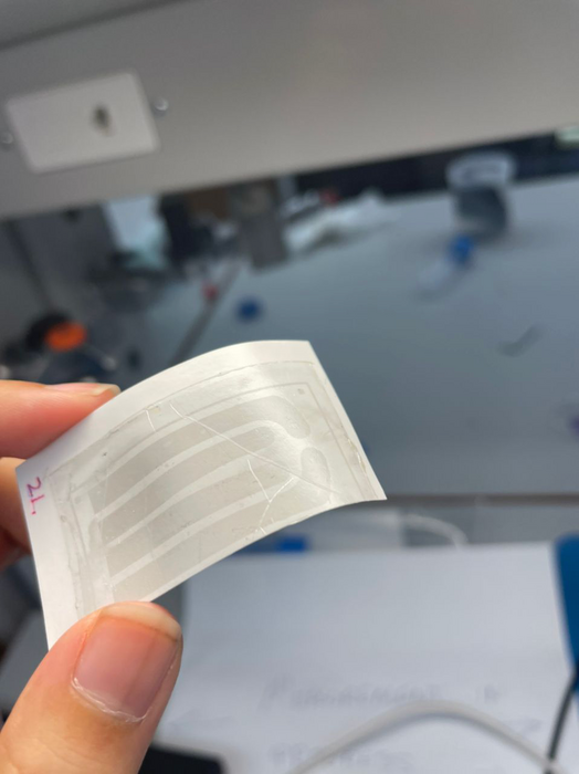
Similar in appearance to a child’s temporary tattoo, the new graphene “tattoo” implant is thinner than a single strand of hair yet still functions like a classical pacemaker. But unlike current pacemakers and implanted defibrillators, which require hard, rigid materials that are mechanically incompatible with the body, the new device softly melds to the heart to simultaneously sense and treat irregular heartbeats. The implant is thin and flexible enough to conform to the heart’s delicate contours as well as stretchy and strong enough to withstand the dynamic motions of a beating heart.

Caption: Graphene implant on tattoo paper. Credit: Ning Liu/University of Texas at Austin

An April 17, 2023 Northwestern University news release (also on EurekAlert), which originated the news item, provides more detail about the research, graphene, and the difficulties of monitoring a beating heart, Note: Links have been removed,

After implanting the device into a rat model, the researchers demonstrated that the graphene tattoo could successfully sense irregular heart rhythms and then deliver electrical stimulation through a series of pulses without constraining or altering the heart’s natural motions. Even better: The technology also is optically transparent, allowing the researchers to use an external source of optical light to record and stimulate the heart through the device.

The study will be published on Thursday (April 20 [2023]) in the journal Advanced Materials. It marks the thinnest known cardiac implant to date.

“One of the challenges for current pacemakers and defibrillators is that they are difficult to affix onto the surface of the heart,” said Northwestern’s Igor Efimov, the study’s senior author. “Defibrillator electrodes, for example, are essentially coils made of very thick wires. These wires are not flexible, and they break. Rigid interfaces with soft tissues, like the heart, can cause various complications. By contrast, our soft, flexible device is not only unobtrusive but also intimately and seamlessly conforms directly onto the heart to deliver more precise measurements.”

An experimental cardiologist, Efimov is a professor of biomedical engineering at Northwestern’s McCormick School of Engineering and professor of medicine at Northwestern University Feinberg School of Medicine. He co-led the study with Dmitry Kireev, a research associate at UT. Zexu Lin, a Ph.D. candidate in Efimov’s laboratory, is the paper’s first author.

Miracle material

Known as cardiac arrhythmias, heart rhythm disorders occur when the heart beats either too quickly or too slowly. While some cases of arrhythmia are not serious, many cases can lead to heart failure, stroke and even sudden death. In fact, complications related to arrythmia claim about 300,000 lives annually in the United States. Physicians commonly treat arrhythmia with implantable pacemakers and defibrillators that detect abnormal heartbeats and then correct rhythm with electrical stimulation. While these devices are lifesaving, their rigid nature may constrain the heart’s natural motions, injure soft tissues, cause temporary discomfort and induce complications, such as painful swelling, perforations, blood clots, infection and more.

With these challenges in mind, Efimov and his team sought to develop a bio-compatible device ideal for conforming to soft, dynamic tissues. After reviewing multiple materials, the researchers settled on graphene, an atomically thin form of carbon. With its ultra-strong, lightweight structure and superior conductivity, graphene has potential for many applications in high-performance electronics, high-strength materials and energy devices.

“For bio-compatibility reasons, graphene is particularly attractive,” Efimov said. “Carbon is the basis of life, so it’s a safe material that is already used in different clinical applications. It also is flexible and soft, which works well as an interface between electronics and a soft, mechanically active organ.”

Hitting a beating target

At UT, study co-authors Dimitry Kireev and Deji Akinwande were already developing graphene electronic tattoos (GETs) with sensing capabilities. Flexible and weightless, their team’s e-tattoos adhere to the skin to continuously monitor the body’s vital signs, including blood pressure and the electrical activity of the brain, heart and muscles.

But, while the e-tattoos work well on the skin’s surface, Efimov’s team needed to investigate new methods to use these devices inside the body — directly onto the surface of the heart.

“It’s a completely different application scheme,” Efimov said. “Skin is relatively dry and easily accessible. Obviously, the heart is inside the chest, so it’s difficult to access and in a wet environment.”

The researchers developed an entirely new technique to encase the graphene tattoo and adhere it to the surface of a beating heart. First, they encapsulated the graphene inside a flexible, elastic silicone membrane — with a hole punched in it to give access to the interior graphene electrode. Then, they gently placed gold tape (with a thickness of 10 microns) onto the encapsulating layer to serve as an electrical interconnect between the graphene and the external electronics used to measure and stimulate the heart. Finally, they placed it onto the heart. The entire thickness of all layers together measures about 100 microns in total.

The resulting device was stable for 60 days on an actively beating heart at body temperature, which is comparable to the duration of temporary pacemakers used as bridges to permanent pacemakers or rhythm management after surgery or other therapies.

Optical opportunities

Leveraging the device’s transparent nature, Efimov and his team performed optocardiography — using light to track and modulate heart rhythm — in the animal study. Not only does this offer a new way to diagnose and treat heart ailments, the approach also opens new possibilities for optogenetics, a method to control and monitor single cells with light. 

While electrical stimulation can correct a heart’s abnormal rhythm, optical stimulation is more precise. With light, researchers can track specific enzymes as well as interrogate specific heart, muscle or nerve cells.

“We can essentially combine electrical and optical functions into one biointerface,” Efimov said. “Because graphene is optically transparent, we can actually read through it, which gives us a much higher density of readout.”

The University of Texas at Austin issued an April 18, 2023 news release and as you would expect the focus is on their researchers, Note 1: I’ve removed many but not all of the redundancies between the two news releases; Note 2: A link has been removed,

A new cardiac implant made from graphene, a two-dimensional super material with ultra-strong, lightweight and conductive properties, functions like a classic pacemaker with some major improvements.

A team led by researchers from The University of Texas at Austin and Northwestern University developed the implantable derivative from wearable graphene-based electronic tattoo, or e-tattoo – graphene biointerface. The device, detailed in the journal Advanced Materials, marks the thinnest known cardiac implant to date.

“It’s very exciting to take our e-tattoo technology and use it as an implantable device inside the body,” said Dmitry Kireev, a postdoctoral research associate in the lab of professor Deji Akinwande’s lab at UT Austin who co-led the research. “The fact that is much more compatible with the human body, lightweight, and transparent, makes this a more natural solution for people dealing with heart problems.”

Hitting a beating target

At UT Austin, Akinwande and his team had been developing e-tattoos using graphene for several years, with a variety of functions, including monitoring body signals. Flexible and weightless, their team’s e-tattoos adhere to the skin to continuously monitor the body’s vital signs, including blood pressure and the electrical activity of the brain, heart and muscles.

But, while the e-tattoos work well on the skin’s surface, the researchers needed to find new ways to deploy these devices inside the body — directly onto the surface of the heart.

“The conditions inside the body are very different compared to affixing a device to the skin, so we had to re-imagine how we package our e-tattoo technology,” said Akinwande, a professor in the Chandra Family Department of Electrical and Computer Engineering.  

The researchers developed an entirely new technique to encase the graphene tattoo and adhere it to the surface of a beating heart. …

Here’s a link to and a citation for the paper,

Graphene Biointerface for Cardiac Arrhythmia Diagnosis and Treatment by Zexu Lin, Dmitry Kireev, Ning Liu, Shubham Gupta, Jessica LaPiano, Sofian N. Obaid, Zhiyuan Chen, Deji Akinwande, Igor R. Efimov. Advanced Materials Volume 35, Issue 22 June 1, 2023 2212190 DOI: https://doi.org/10.1002/adma.202212190 First published online: 25 March 2023

This paper is open access.

Enabling a transparent wood battery that stores heat and regulates indoor temperature with lemons and coconuts

i’ve had transparent wood stories here before but this time it was the lemons and coconuts which captured my attention.

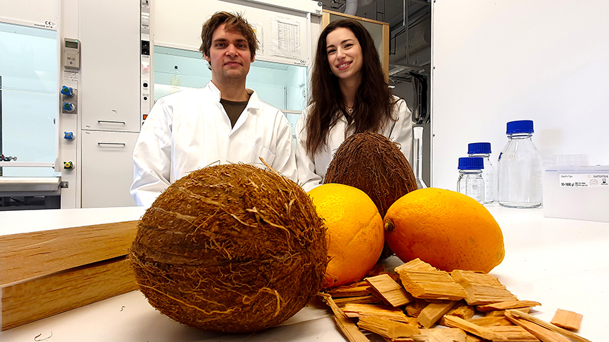
Peter Olsén and Céline Montanari, researchers in the Department of Biocomposites at KTH Royal Institute of Technology in Stockholm, say the new wood composite uses components of lemon and coconuts to both heat and cool homes. (Photo: David Callahan) Courtesy: KTH Royal Institute of Technology

From a March 30, 2023 news item on Nanowerk,

A building material that combines coconuts, lemons and modified wood could one day be enough to heat and cool your home. The three renewable sources provide the key components of a wood composite thermal battery, which was developed by researchers at KTH Royal Institute of Technology in Stockholm.

Researchers reported the development in the scientific journal, Small (“Sustainable Thermal Energy Batteries from Fully Bio-Based Transparent Wood”). Peter Olsén, researcher in the Department of Biocomposites at KTH, says the material is capable of storing both heat and cold. If used in housing construction, the researchers say that 100 kilos of the material can save about 2.5 kWh per day in heating or cooling—given an ambient temperature of 24 °C.

KTH researcher Céline Montanari says that besides sunlight, any heat source can charge the battery. “The key is that the temperature fluctuates around the transition temperature, 24 °C, which can of course be tailored depending on the application and location,” she says.

A March 30, 2023 KTH Royal Institute of Technology press release, which originated the news item, describes the roles that lemons and coconuts play,

The process starts with removing lignin from wood, which creates open pores in the wood cells walls, and removes color. Later the wood structure is filled with a citrus-based molecule—limonene acrylate—and coconut based molecule. Limonene acrylate transforms into a bio-based polymer when heated, restoring the wood’s strength and allowing light to permeate. When this happens the coconut molecule are trapped within the material, enabling the storage and release of energy.

“The elegance is that the coconut molecules can transition from a solid-to-liquid which absorbs energy; or from liquid-to-solid which releases energy, in much the same way that water freezes and melts,” Montanari says. But in the transparent wood, that transition happens at a more comfortable 24C

“Through this transition, we can heat or cool our surroundings, whichever is needed,” Olsén says

Olsén says that potential uses include exterior and interior building material for both transparency and energy saving – in exteriors and interiors. The first application of the product would be for interior spaces to regulate temperatures around the 24C mark to cool and to heat. More study is needed to develop it for exterior use.

And it’s not just for homes or buildings. “Why not as a future material in greenhouses?” he says. “When the sun shines, the wood becomes transparent and stores more energy, while at night it becomes cloudy and releases the heat stored during the day. That would help reduce energy consumption for heating and at the same time provide improved growth.”

A close-up look at the material produced in the study. Courtesy: KTH Royal Institute of Technology

Here’s a link to and a citation for the paper,

Sustainable Thermal Energy Batteries from Fully Bio-Based Transparent Wood by Céline Montanari, Hui Chen, Matilda Lidfeldt, Josefin Gunnarsson, Peter Olsén, Lars A. Berglund. Small Online Version of Record before inclusion in an issue 2301262 DOI: https://doi.org/10.1002/smll.202301262 First published online: 27 March 2023

This paper is open access.

Smart fabric from University of Waterloo (Canada) responds to temperature and electricity

This textile from the University of Waterloo is intriguing,

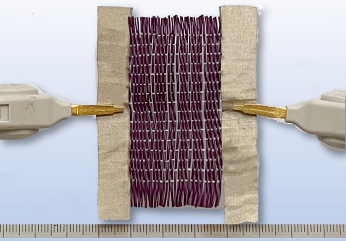
Caption: An electric current is applied to an engineered smart fabric consisting of plastic and steel fibres. Credit: University of Waterloo

An April 24, 2023 news item on phys.org introduces this new material,

A new smart material developed by researchers at the University of Waterloo is activated by both heat and electricity, making it the first ever to respond to two different stimuli.

The unique design paves the way for a wide variety of potential applications, including clothing that warms up while you walk from the car to the office in winter and vehicle bumpers that return to their original shape after a collision.

An April 24, 2023 University of Waterloo news release (also on EurekAlert), which originated the news item, provides more detail, Note: A link has been removed,

Inexpensively made with polymer nano-composite fibres from recycled plastic, the programmable fabric can change its colour and shape when stimuli are applied.

“As a wearable material alone, it has almost infinite potential in AI, robotics and virtual reality games and experiences,” said Dr. Milad Kamkar, a chemical engineering professor at Waterloo. “Imagine feeling warmth or a physical trigger eliciting a more in-depth adventure in the virtual world.”

The novel fabric design is a product of the happy union of soft and hard materials, featuring a combination of highly engineered polymer composites and stainless steel in a woven structure. 

Researchers created a device similar to a traditional loom to weave the smart fabric. The resulting process is extremely versatile, enabling design freedom and macro-scale control of the fabric’s properties.

The fabric can also be activated by a lower voltage of electricity than previous systems, making it more energy-efficient and cost-effective. In addition, lower voltage allows integration into smaller, more portable devices, making it suitable for use in biomedical devices and environment sensors.

“The idea of these intelligent materials was first bred and born from biomimicry science,” said Kamkar, director of the Multi-scale Materials Design (MMD) Centre at Waterloo.

“Through the ability to sense and react to environmental stimuli such as temperature, this is proof of concept that our new material can interact with the environment to monitor ecosystems without damaging them.”

The next step for researchers is to improve the fabric’s shape-memory performance for applications in the field of robotics. The aim is to construct a robot that can effectively carry and transfer weight to complete tasks.

Here’s a link to and a citation for the paper,

Multi-Stimuli Dually-Responsive Intelligent Woven Structures with Local Programmability for Biomimetic Applications by Runxin Xu, Guanzheng Wu, Mengmeng Jiang, Shaojie Cao, Mahyar Panahi-Sarmad, Milad Kamkar, Xueliang Xiao. Nano-Micro Small DOI: https://doi.org/10.1002/smll.202207900 First published: 19 February 2023

This paper is open access.

Combining silicon with metal oxide memristors to create powerful, low-energy intensive chips enabling AI in portable devices

In this one week, I’m publishing my first stories (see also June 13, 2023 posting “ChatGPT and a neuromorphic [brainlike] synapse“) where artificial intelligence (AI) software is combined with a memristor (hardware component) for brainlike (neuromorphic) computing.

Here’s more about some of the latest research from a March 30, 2023 news item on ScienceDaily,

Everyone is talking about the newest AI and the power of neural networks, forgetting that software is limited by the hardware on which it runs. But it is hardware, says USC [University of Southern California] Professor of Electrical and Computer Engineering Joshua Yang, that has become “the bottleneck.” Now, Yang’s new research with collaborators might change that. They believe that they have developed a new type of chip with the best memory of any chip thus far for edge AI (AI in portable devices).

A March 29, 2023 University of Southern California (USC) news release (also on EurekAlert), which originated the news item, contextualizes the research and delves further into the topic of neuromorphic hardware,

For approximately the past 30 years, while the size of the neural networks needed for AI and data science applications doubled every 3.5 months, the hardware capability needed to process them doubled only every 3.5 years. According to Yang, hardware presents a more and more severe problem for which few have patience. 

Governments, industry, and academia are trying to address this hardware challenge worldwide. Some continue to work on hardware solutions with silicon chips, while others are experimenting with new types of materials and devices.  Yang’s work falls into the middle—focusing on exploiting and combining the advantages of the new materials and traditional silicon technology that could support heavy AI and data science computation. 

Their new paper in Nature focuses on the understanding of fundamental physics that leads to a drastic increase in memory capacity needed for AI hardware. The team led by Yang, with researchers from USC (including Han Wang’s group), MIT [Massachusetts Institute of Technology], and the University of Massachusetts, developed a protocol for devices to reduce “noise” and demonstrated the practicality of using this protocol in integrated chips. This demonstration was made at TetraMem, a startup company co-founded by Yang and his co-authors  (Miao Hu, Qiangfei Xia, and Glenn Ge), to commercialize AI acceleration technology. According to Yang, this new memory chip has the highest information density per device (11 bits) among all types of known memory technologies thus far. Such small but powerful devices could play a critical role in bringing incredible power to the devices in our pockets. The chips are not just for memory but also for the processor. And millions of them in a small chip, working in parallel to rapidly run your AI tasks, could only require a small battery to power it. 

The chips that Yang and his colleagues are creating combine silicon with metal oxide memristors in order to create powerful but low-energy intensive chips. The technique focuses on using the positions of atoms to represent information rather than the number of electrons (which is the current technique involved in computations on chips). The positions of the atoms offer a compact and stable way to store more information in an analog, instead of digital fashion. Moreover, the information can be processed where it is stored instead of being sent to one of the few dedicated ‘processors,’ eliminating the so-called ‘von Neumann bottleneck’ existing in current computing systems.  In this way, says Yang, computing for AI is “more energy efficient with a higher throughput.”

How it works: 

Yang explains that electrons which are manipulated in traditional chips, are “light.” And this lightness, makes them prone to moving around and being more volatile.  Instead of storing memory through electrons, Yang and collaborators are storing memory in full atoms. Here is why this memory matters. Normally, says Yang, when one turns off a computer, the information memory is gone—but if you need that memory to run a new computation and your computer needs the information all over again, you have lost both time and energy.  This new method, focusing on activating atoms rather than electrons, does not require battery power to maintain stored information. Similar scenarios happen in AI computations, where a stable memory capable of high information density is crucial. Yang imagines this new tech that may enable powerful AI capability in edge devices, such as Google Glasses, which he says previously suffered from a frequent recharging issue.

Further, by converting chips to rely on atoms as opposed to electrons, chips become smaller.  Yang adds that with this new method, there is more computing capacity at a smaller scale. And this method, he says, could offer “many more levels of memory to help increase information density.” 

To put it in context, right now, ChatGPT is running on a cloud. The new innovation, followed by some further development, could put the power of a mini version of ChatGPT in everyone’s personal device. It could make such high-powered tech more affordable and accessible for all sorts of applications. 

Here’s a link to and a citation for the paper,

Thousands of conductance levels in memristors integrated on CMOS by Mingyi Rao, Hao Tang, Jiangbin Wu, Wenhao Song, Max Zhang, Wenbo Yin, Ye Zhuo, Fatemeh Kiani, Benjamin Chen, Xiangqi Jiang, Hefei Liu, Hung-Yu Chen, Rivu Midya, Fan Ye, Hao Jiang, Zhongrui Wang, Mingche Wu, Miao Hu, Han Wang, Qiangfei Xia, Ning Ge, Ju Li & J. Joshua Yang. Nature volume 615, pages 823–829 (2023) DOI: https://doi.org/10.1038/s41586-023-05759-5 Issue Date: 30 March 2023 Published: 29 March 2023

This paper is behind a paywall.

ChatGPT and a neuromorphic (brainlike) synapse

I was teaching an introductory course about nanotechnology back in 2014 and, at the end of a session, stated (more or less) that the full potential for artificial intelligence (software) wasn’t going to be perceived until the hardware (memistors) was part of the package. (It’s interesting to revisit that in light of the recent uproar around AI (covered in my May 25, 2023 posting, which offered a survey of the situation.)

One of the major problems with artificial intelligence is its memory. The other is energy consumption. Both problems could be addressed by the integration of memristors into the hardware, giving rise to neuromorphic (brainlike) computing. (For those who don’t know, the human brain in addition to its capacity for memory is remarkably energy efficient.)

This is the first time I’ve seen research into memristors where software has been included. Disclaimer: There may be a lot more research of this type; I just haven’t seen it before. A March 24, 2023 news item on ScienceDaily announces research from Korea,

ChatGPT’s impact extends beyond the education sector and is causing significant changes in other areas. The AI language model is recognized for its ability to perform various tasks, including paper writing, translation, coding, and more, all through question-and-answer-based interactions. The AI system relies on deep learning, which requires extensive training to minimize errors, resulting in frequent data transfers between memory and processors. However, traditional digital computer systems’ von Neumann architecture separates the storage and computation of information, resulting in increased power consumption and significant delays in AI computations. Researchers have developed semiconductor technologies suitable for AI applications to address this challenge.

A March 24, 2023 Pohang University of Science & Technology (POSTECH) press release (also on EurekAlert), which originated the news item, provides more detail,

A research team at POSTECH, led by Professor Yoonyoung Chung (Department of Electrical Engineering, Department of Semiconductor Engineering), Professor Seyoung Kim (Department of Materials Science and Engineering, Department of Semiconductor Engineering), and Ph.D. candidate Seongmin Park (Department of Electrical Engineering), has developed a high-performance AI semiconductor device [emphasis mine] using indium gallium zinc oxide (IGZO), an oxide semiconductor widely used in OLED [organic light-emitting diode] displays. The new device has proven to be excellent in terms of performance and power efficiency.

Efficient AI operations, such as those of ChatGPT, require computations to occur within the memory responsible for storing information. Unfortunately, previous AI semiconductor technologies were limited in meeting all the requirements, such as linear and symmetric programming and uniformity, to improve AI accuracy.

The research team sought IGZO as a key material for AI computations that could be mass-produced and provide uniformity, durability, and computing accuracy. This compound comprises four atoms in a fixed ratio of indium, gallium, zinc, and oxygen and has excellent electron mobility and leakage current properties, which have made it a backplane of the OLED display.

Using this material, the researchers developed a novel synapse device [emphasis mine] composed of two transistors interconnected through a storage node. The precise control of this node’s charging and discharging speed has enabled the AI semiconductor to meet the diverse performance metrics required for high-level performance. Furthermore, applying synaptic devices to a large-scale AI system requires the output current of synaptic devices to be minimized. The researchers confirmed the possibility of utilizing the ultra-thin film insulators inside the transistors to control the current, making them suitable for large-scale AI.

The researchers used the newly developed synaptic device to train and classify handwritten data, achieving a high accuracy of over 98%, [emphasis mine] which verifies its potential application in high-accuracy AI systems in the future.

Professor Chung explained, “The significance of my research team’s achievement is that we overcame the limitations of conventional AI semiconductor technologies that focused solely on material development. To do this, we utilized materials already in mass production. Furthermore, Linear and symmetrical programming characteristics were obtained through a new structure using two transistors as one synaptic device. Thus, our successful development and application of this new AI semiconductor technology show great potential to improve the efficiency and accuracy of AI.”

This study was published last week [March 2023] on the inside back cover of Advanced Electronic Materials [paper edition] and was supported by the Next-Generation Intelligent Semiconductor Technology Development Program through the National Research Foundation, funded by the Ministry of Science and ICT [Information and Communication Technologies] of Korea.

Here’s a link to and a citation for the paper,

Highly Linear and Symmetric Analog Neuromorphic Synapse Based on Metal Oxide Semiconductor Transistors with Self-Assembled Monolayer for High-Precision Neural Network Computatio by Seongmin Park, Suwon Seong, Gilsu Jeon, Wonjae Ji, Kyungmi Noh, Seyoung Kim, Yoonyoung Chun. Volume 9, Issue 3 March 2023 2200554 DOI: https://doi.org/10.1002/aelm.202200554 First published online: 29 December 2022

This paper is open access.

Also, there is another approach to using materials such as indium gallium zinc oxide (IGZO) for a memristor. That would be using biological cells as my June 6, 2023 posting, which features work on biological neural networks (BNNs), suggests in relation to creating robots that can perform brainlike computing.

Future firefighters and wearable technology

I imagine this wearable technology would also be useful for the military too. However, the focus for these researchers from China is firefighting. (Given the situation with the Canadian wildfires in June 2023, we have 10x more than the average at this time in the season over the last 10 years, it’s good to see some work focused on safety for firefighters.) From a January 17, 2023 news item on phys.org,

Firefighting may look vastly different in the future thanks to intelligent fire suits and masks developed by multiple research institutions in China.

Researchers published results showing breathable electrodes woven into fabric used in fire suits have proven to be stable at temperatures over 520ºC. At these temperatures, the fabric is found to be essentially non-combustible with high rates of thermal protection time.

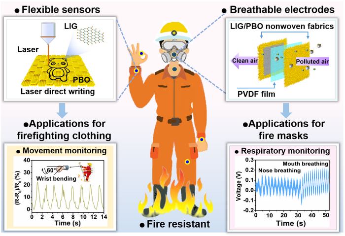
Caption: Scientists from multiple institutions address the challenges and limitations of current fire-fighting gear by introducing wearable, breathable sensors and electrodes to better serve firefighters. Credit: Nano Research, Tsinghua University Press

A January 17, 2023 Tsinghua University Press press release on EurekAlert, which originated the news item, provides more technical details,

The results show the efficacy and practicality of Janus graphene/poly(p-phenylene benzobisoxazole), or PBO, woven fabric in making firefighting “smarter” with the main goal being to manufacture products on an industrial scale that are flame-retardant but also intelligent enough to warn the firefighter of increased risks while traversing the flames.

“Conventional firefighting clothing and fire masks can ensure firemen’s safety to a certain extent,” said Wei Fan, professor at the School of Textile Science and Engineering at Xi’an Polytechnic University. “However, the fire scene often changes quickly, sometimes making firefighters trapped in the fire for failing to judge the risks in time. At this situation, firefighters also need to be rescued.”

The key here is the use of Janus graphene/PBO, woven fabrics. While not the first of its kind, the introduction of PBO fibers offers better strength and fire protection than other similar fibers, such as Kevlar. The PBO fibers are first woven into a fabric that is then irradiated using a CO2 infrared laser. From here, the fabric becomes the Janus graphene/PBO hybrid that is the focus of the study.   

The mask also utilizes a top and bottom layer of Janus graphene/PBO with a piezoelectric layer in between that acts as a way to convert mechanical pressures to electricity.

“The mask has a good smoke particle filtration effect, and the filtration efficiency of PM2.5 and PM3.0 reaches 95% and 100%, respectively. Meanwhile, the mask has good wearing comfort as its respiratory resistance (46.8 Pa) is lower than 49 Pa of commercial masks. Besides, the mask is sensitive to the speed and intensity of human breathing, which can dynamically monitor the health of the firemen” said Fan.

Flame-retardant electronics featured in these fire suits are flexible, heat resistant, quick to make and low-cost which makes scaling for industrial production a tangible achievement. This makes it more likely that the future of firefighting suits and masks will be able to effectively use this technology. Quick, effective responses can also reduce economic losses attributed to fires.

“The graphene/PBO woven fabrics-based sensors exhibit good repeatability and stability in human motion monitoring and NO2 gas detection, the main toxic gas in fires, which can be applied to firefighting suits to help firefighters effectively avoiding danger” Fan said. Being able to detect sharp increases in NO2 gas can help firefighters change course in an instant if needed and could be a lifesaving addition to firefighter gear.

Major improvements can be made in the firefighting field to better protect the firefighters by taking advantage of graphene/PBO woven and nonwoven fabrics. Widescale use of this technology can help the researchers reach their ultimate goal of reducing mortality and injury to those who risk their lives fighting fires.

Yu Luo and Yaping Miao of the School of Textile Science and Engineering at Xi’an Polytechnic University contributed equally to this work. Professor Wei Fan is the corresponding author. Yingying Zhang and Huimin Wang of the Department of Chemistry at Tsinghua University, Kai Dong of the Beijing Institute of Nanoenergy and Nanosystems at the Chinese Academy of Sciences, and Lin Hou and Yanyan Xu of Shaanxi Textile Research Institute Co., LTD, Weichun Chen and Yao Zhang of the School of Textile Science and Engineering at Xi’an Polytechnic University contributed to this research. 

This work was supported by the National Natural Science Foundation of China, Textile Vision Basic Research Program of China, Key Research and Development Program of Xianyang Science and Technology Bureau, Key Research and Development Program of Shaanxi Province, Natural Science Foundation of Shaanxi Province, and Scientific Research Project of Shaanxi Provincial Education Department.

Here are two links and a citation for the same paper,

Laser-induced Janus graphene/poly(p-phenylene benzobisoxazole) fabrics with intrinsic flame retardancy as flexible sensors and breathable electrodes for fire-fighting field by Yu Luo, Yaping Miao, Huimin Wang, Kai Dong, Lin Hou, Yanyan Xu, Weichun Chen, Yao Zhang, Yingying Zhang & Wei Fan. Nano Research (2023) DOI: https://doi.org/10.1007/s12274-023-5382-y Published12 January 2023

This link leads to a paywall.

Here’s the second link (to SciOpen)

Laser-induced Janus graphene/poly(p-phenylene benzobisoxazole) fabrics with intrinsic flame retardancy as flexible sensors and breathable electrodes for fire-fighting field. SciOpen Published January 12, 2023

This link leads to an open access journal published by Tsinghua University Press.