Monthly Archives: September 2016

Long-term brain mapping with injectable electronics

Charles Lieber and his team at Harvard University announced a success with their work on injectable electronics last year (see my June 11, 2015 posting for more) and now they are reporting on their work with more extensive animal studies according to an Aug. 29, 2016 news item on psypost.org,

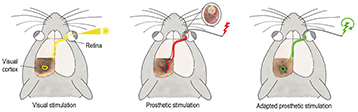
Scientists in recent years have made great strides in the quest to understand the brain by using implanted probes to explore how specific neural circuits work.

Though effective, those probes also come with their share of problems as a result of rigidity. The inflammation they produce induces chronic recording instability and means probes must be relocated every few days, leaving some of the central questions of neuroscience – like how the neural circuits are reorganized during development, learning and aging- beyond scientists’ reach.

But now, it seems, things are about to change.

Led by Charles Lieber, The Mark Hyman Jr. Professor of Chemistry and chair of the Department of Chemistry and Chemical Biology, a team of researchers that included graduate student Tian-Ming Fu, postdoctoral fellow Guosong Hong, graduate student Tao Zhou and others, has demonstrated that syringe-injectable mesh electronics can stably record neural activity in mice for eight months or more, with none of the inflammation

An Aug. 29, 2016 Harvard University press release, which originated the news item, provides more detail,

“With the ability to follow the same individual neurons in a circuit chronically…there’s a whole suite of things this opens up,” Lieber said. “The eight months we demonstrate in this paper is not a limit, but what this does show is that mesh electronics could be used…to investigate neuro-degenerative diseases like Alzheimer’s, or processes that occur over long time, like aging or learning.”

Lieber and colleagues also demonstrated that the syringe-injectable mesh electronics could be used to deliver electrical stimulation to the brain over three months or more.

“Ultimately, our aim is to create these with the goal of finding clinical applications,” Lieber said. “What we found is that, because of the lack of immune response (to the mesh electronics), which basically insulates neurons, we can deliver stimulation in a much more subtle way, using lower voltages that don’t damage tissue.”

The possibilities, however, don’t end there.

The seamless integration of the electronics and biology, Lieber said, could open the door to an entirely new class of brain-machine interfaces and vast improvements in prosthetics, among other fields.

“Today, brain-machine interfaces are based on traditional implanted probes, and there has been some impressive work that’s been done in that field,” Lieber said. “But all the interfaces rely on the same technique to decode neural signals.”

Because traditional rigid implanted probes are invariably unstable, he explained, researchers and clinicians rely on decoding what they call the “population average” – essentially taking a host of neural signals and applying complex computational tools to determine what they mean.

Using tissue-like mesh electronics, by comparison, researchers may be able to read signals from specific neurons over time, potentially allowing for the development of improved brain-machine interfaces for prosthetics.

“We think this is going to be very powerful, because we can identify circuits and both record and stimulate in a way that just hasn’t been possible before,” Lieber said. “So what I like to say is: I think therefore it happens.”

Lieber even held out the possibility that the syringe-injectable mesh electronics could one day be used to treat catastrophic injuries to the brain and spinal cord.

“I don’t think that’s science-fiction,” he said. “Other people may say that will be possible through, for example, regenerative medicine, but we are pursuing this from a different angle.

“My feeling is that this is about a seamless integration between the biological and the electronic systems, so they’re not distinct entities,” he continued. “If we can make the electronics look like the neural network, they will work together…and that’s where you want to be if you want to exploit the strengths of both.”

In the 2015 posting, Lieber was discussing cyborgs, here he broaches the concept without using the word, “… seamless integration between the biological and the electronic systems, so they’re not distinct entities.”

Here’s a link to and a citation for the paper,

Stable long-term chronic brain mapping at the single-neuron level by Tian-Ming Fu, Guosong Hong, Tao Zhou, Thomas G Schuhmann, Robert D Viveros, & Charles M Lieber. Nature Methods (2016) doi:10.1038/nmeth.3969 Published online 29 August 2016

This paper is behind a paywall.

Teleporting photons in Calgary (Canada) is a step towards a quantum internet

Scientists at the University of Calgary (Alberta, Canada) have set a distance record for the teleportation of photons and you can see the lead scientist is very pleased.

Wolfgang Tittel, professor of physics and astronomy at the University of Calgary, and a group of PhD students have developed a new quantum key distribution (QKD) system.

Wolfgang Tittel, professor of physics and astronomy at the University of Calgary, and a group of PhD students have developed a new quantum key distribution (QKD) system.

A Sept. 21, 2016 news item on phys.org makes the announcement (Note: A link has been removed),

What if you could behave like the crew on the Starship Enterprise and teleport yourself home or anywhere else in the world? As a human, you’re probably not going to realize this any time soon; if you’re a photon, you might want to keep reading.

Through a collaboration between the University of Calgary, The City of Calgary and researchers in the United States, a group of physicists led by Wolfgang Tittel, professor in the Department of Physics and Astronomy at the University of Calgary have successfully demonstrated teleportation of a photon (an elementary particle of light) over a straight-line distance of six kilometres using The City of Calgary’s fibre optic cable infrastructure. The project began with an Urban Alliance seed grant in 2014.

This accomplishment, which set a new record for distance of transferring a quantum state by teleportation, has landed the researchers a spot in the prestigious Nature Photonics scientific journal. The finding was published back-to-back with a similar demonstration by a group of Chinese researchers.

A Sept. 20, 2016 article by Robson Fletcher for CBC (Canadian Broadcasting News) online provides a bit more insight from the lead researcher (Note: A link has been removed),

“What is remarkable about this is that this information transfer happens in what we call a disembodied manner,” said physics professor Wolfgang Tittel, whose team’s work was published this week in the journal Nature Photonics.

“Our transfer happens without any need for an object to move between these two particles.”

A Sept. 20, 2016 University of Calgary news release by Drew Scherban, which originated the news item, provides more insight into the research,

“Such a network will enable secure communication without having to worry about eavesdropping, and allow distant quantum computers to connect,” says Tittel.

Experiment draws on ‘spooky action at a distance’

The experiment is based on the entanglement property of quantum mechanics, also known as “spooky action at a distance” — a property so mysterious that not even Einstein could come to terms with it.

“Being entangled means that the two photons that form an entangled pair have properties that are linked regardless of how far the two are separated,” explains Tittel. “When one of the photons was sent over to City Hall, it remained entangled with the photon that stayed at the University of Calgary.”

Next, the photon whose state was teleported to the university was generated in a third location in Calgary and then also travelled to City Hall where it met the photon that was part of the entangled pair.

“What happened is the instantaneous and disembodied transfer of the photon’s quantum state onto the remaining photon of the entangled pair, which is the one that remained six kilometres away at the university,” says Tittel.

City’s accessible dark fibre makes research possible

The research could not be possible without access to the proper technology. One of the critical pieces of infrastructure that support quantum networking is accessible dark fibre. Dark fibre, so named because of its composition — a single optical cable with no electronics or network equipment on the alignment — doesn’t interfere with quantum technology.

The City of Calgary is building and provisioning dark fibre to enable next-generation municipal services today and for the future.

“By opening The City’s dark fibre infrastructure to the private and public sector, non-profit companies, and academia, we help enable the development of projects like quantum encryption and create opportunities for further research, innovation and economic growth in Calgary,” said Tyler Andruschak, project manager with Innovation and Collaboration at The City of Calgary.

“The university receives secure access to a small portion of our fibre optic infrastructure and The City may benefit in the future by leveraging the secure encryption keys generated out of the lab’s research to protect our critical infrastructure,” said Andruschak. In order to deliver next-generation services to Calgarians, The City has been increasing its fibre optic footprint, connecting all City buildings, facilities and assets.

Timed to within one millionth of one millionth of a second

As if teleporting a photon wasn’t challenging enough, Tittel and his team encountered a number of other roadblocks along the way.

Due to changes in the outdoor temperature, the transmission time of photons from their creation point to City Hall varied over the course of a day — the time it took the researchers to gather sufficient data to support their claim. This change meant that the two photons would not meet at City Hall.

“The challenge was to keep the photons’ arrival time synchronized to within 10 pico-seconds,” says Tittel. “That is one trillionth, or one millionth of one millionth of a second.”

Secondly, parts of their lab had to be moved to two locations in the city, which as Tittel explains was particularly tricky for the measurement station at City Hall which included state-of-the-art superconducting single-photon detectors developed by the National Institute for Standards and Technology, and NASA’s Jet Propulsion Laboratory.

“Since these detectors only work at temperatures less than one degree above absolute zero the equipment also included a compact cryostat,” said Tittel.

Milestone towards a global quantum Internet

This demonstration is arguably one of the most striking manifestations of a puzzling prediction of quantum mechanics, but it also opens the path to building a future quantum internet, the long-term goal of the Tittel group.

The Urban Alliance is a strategic research partnership between The City of Calgary and University of Calgary, created in 2007 to encourage and co-ordinate the seamless transfer of cutting-edge research between the university and The City of Calgary for the benefit of all our communities. The Urban Alliance is a prime example and vehicle for one of the three foundational commitments of the University of Calgary’s Eyes High vision to fully integrate the university with the community. The City sees the Alliance as playing a key role in realizing its long-term priorities and the imagineCALGARY vision.

Here’s a link to and a citation for the paper,

Quantum teleportation across a metropolitan fibre network by Raju Valivarthi, Marcel.li Grimau Puigibert, Qiang Zhou, Gabriel H. Aguilar, Varun B. Verma, Francesco Marsili, Matthew D. Shaw, Sae Woo Nam, Daniel Oblak, & Wolfgang Tittel. Nature Photonics (2016)  doi:10.1038/nphoton.2016.180 Published online 19 September 2016

This paper is behind a paywall.

I’m 99% certain this is the paper from the Chinese researchers (referred to in the University of Calgary news release),

Quantum teleportation with independent sources and prior entanglement distribution over a network by Qi-Chao Sun, Ya-Li Mao, Si-Jing Chen, Wei Zhang, Yang-Fan Jiang, Yan-Bao Zhang, Wei-Jun Zhang, Shigehito Miki, Taro Yamashita, Hirotaka Terai, Xiao Jiang, Teng-Yun Chen, Li-Xing You, Xian-Feng Chen, Zhen Wang, Jing-Yun Fan, Qiang Zhang & Jian-Wei Pan. Nature Photonics (2016)  doi:10.1038/nphoton.2016.179 Published online 19 September 2016

This too is behind a paywall.

Reliable findings on the presence of synthetic (engineered) nanoparticles in bodies of water

An Aug. 29, 2016 news item on Nanowerk announces research into determining the presence of engineered (synthetic) nanoparticles in bodies of water,

For a number of years now, an increasing number of synthetic nanoparticles have been manufactured and incorporated into various products, such as cosmetics. For the first time, a research project at the Technical University of Munich and the Bavarian Ministry of the Environment provides reliable findings on their presence in water bodies.

An Aug. 29, 2016 Technical University of Munich (TUM) press release, which originated the news item, provides more information,

Nanoparticles can improve the properties of materials and products. That is the reason why an increasing number of nanoparticles have been manufactured over the past several years. The worldwide consumption of silver nanoparticles is currently estimated at over 300 metric tons. These nanoparticles have the positive effect of killing bacteria and viruses. Products that are coated with these particles include refrigerators and surgical instruments. Silver nanoparticles can even be found in sportswear. This is because the silver particles can prevent the smell of sweat by killing the bacteria that cause it.

Previously, it was unknown whether and in what concentration these nanoparticles enter the environment and e.g. enter bodies of water. If they do, this poses a problem. That is because the silver nanoparticles are toxic to numerous aquatic organisms, and can upset sensitive ecological balances.

Analytical challenge

In the past, however, nanoparticles have not been easy to detect. That is because they measure only 1 to 100 nanometers across [nanoparticles may be larger than 100nm or smaller than 1nm but the official definitions usually specify up to 100nm although some definitions go up to 1000nm] – a nanometer is a millionth of a millimeter. “In order to know if a toxicological hazard exists, we need to know how many of these particles enter the environment, and in particular bodies of water”, explains Michael Schuster, Professor for Analytical Chemistry at the TU Munich.

This was an analytical challenge for the researchers charged with solving the problem on behalf of the Bavarian Ministry of the Environment. In order to overcome this issue, they used a well-known principle that utilizes the effect of surfactants to separate and concentrate the particles. “Surfactants are also found in washing and cleaning detergents”, explains Schuster. “Basically, what they do is envelop grease and dirt particles in what are called micelles, making it possible for them to float in water.” One side of the surfactant is water-soluble, the other fat-soluble. The fat-soluble ends collect around non-polar, non-water soluble compounds such as grease or around particles, and “trap” them in a micelle. The water-soluble, polar ends of the surfactants, on the other hand, point towards the water molecules, allowing the microscopically small micelle to float in water.

A box of sugar cubes in the Walchensee lake

The researchers applied this principle to the nanoparticles. “When the micelles surrounding the particles are warmed slightly, they start to clump”, explains Schuster. This turns the water cloudy. Using a centrifuge, the surfactants and the nanoparticles trapped in them can then be separated from the water. This procedure is called cloud point extraction. The researchers then use the surfactants that have been separated out in this manner – which contain the particles in an unmodified, but highly concentrated form – to measure how many silver nanoparticles are present. To do this, they use a highly sensitive atomic spectrometer configured to only detect silver. In this manner, concentrations in a range of less than one nanogram per liter can be detected. To put this in perspective, this would be like detecting a box of sugar cubes that had dissolved in the Walchensee lake.

With the help of this analysis procedure, it is possible to gain new insight into the concentration of nanoparticles in drinking and waste water, sewage sludge, rivers, and lakes. In Bavaria, the measurements yielded good news: The concentrations measured in the water bodies were extremely low. In was only in four of the 13 Upper Bavarian lakes examined that the concentration even exceeded the minimum detection limit of 0.2 nanograms per liter. No measured value exceeded 1.3 nanograms per liter. So far, no permissible values have been established for silver nanoparticles.

Representative for watercourses, the Isar river was examined from its source to its mouth at around 30 locations. The concentration of silver nanoparticles was also measured in the inflow and outflow of sewage treatment plants. The findings showed that at least 94 percent of silver nanoparticles are filtered out by the sewage treatment plants.

Unfortunately, the researchers have not published their results.

Harvard University announced new Center on Nano-safety Research

The nano safety center at Harvard University (Massachusetts, US) is a joint center with the US National Institute of Environmental Health  Sciences according to an Aug. 29, 2016 news item on Nanowerk,

Engineered nanomaterials (ENMs)—which are less than 100 nanometers (one millionth of a millimeter) in diameter—can make the colors in digital printer inks pop and help sunscreens better protect against radiation, among many other applications in industry and science. They may even help prevent infectious diseases. But as the technology becomes more widespread, questions remain about the potential risks that ENMs may pose to health and the environment.

Researchers at the new Harvard-NIEHS [US National Institute of Environmental Health Sciences] Nanosafety Research Center at Harvard T.H. Chan School of Public Health are working to understand the unique properties of ENMs—both beneficial and harmful—and to ultimately establish safety standards for the field.

An Aug. 16, 2016 Harvard University press release, which originated the news item, provides more detail (Note: Links have been removed),

“We want to help nanotechnology develop as a scientific and economic force while maintaining safeguards for public health,” said Center Director Philip Demokritou, associate professor of aerosol physics at Harvard Chan School. “If you understand the rules of nanobiology, you can design safer nanomaterials.”

ENMs can enter the body through inhalation, ingestion, and skin contact, and toxicological studies have shown that some can penetrate cells and tissues and potentially cause biochemical damage. Because the field of nanoparticle science is relatively new, no standards currently exist for assessing the health risks of exposure to ENMs—or even for how studies of nano-biological interactions should be conducted.

Much of the work of the new Center will focus on building a fundamental understanding of why some ENMs are potentially more harmful than others. The team will also establish a “reference library” of ENMs, each with slightly varied properties, which will be utilized in nanotoxicology research across the country to assess safety. This will allow researchers to pinpoint exactly what aspect of an ENM’s properties may impact health. The researchers will also work to develop standardized methods for nanotoxicology studies evaluating the safety of nanomaterials.

The Center was established with a $4 million dollar grant from the National Institute of Environmental Health Science (NIEHS) last month, and is the only nanosafety research center to receive NIEHS funding for the next five years. It will also play a coordinating role with existing and future NIEHS nanotoxicology research projects nantionwide. Scientists from the Harvard John A. Paulson School of Engineering and Applied Sciences (SEAS), MIT, University of Maine, and University of Florida will collaborate on the new effort.

The Center builds on the existing Center for Nanotechnology and Nanotoxicology at Harvard Chan School, established by Demokritou and Joseph Brain, Cecil K. and Philip Drinker Professor of Environmental Physiology, in the School’s Department of Environmental Health in 2010.

A July 5, 2016 Harvard University press release announcing the $4M grant provides more information about which ENMs are to be studied,

The main focus of the new HSPH-NIEHS Center is to bring together  scientists from across disciplines- material science, chemistry, exposure assessment, risk assessment, nanotoxicology and nanobiology- to assess the potential  environmental Health and safety (EHS) implications of engineered nanomaterials (ENMs).

The $4 million dollar HSPH based Center  which is the only Nanosafety Research  Center to be funded by NIEHS this funding cycle, … The new HSPH-NIEHS Nanosafety Center builds upon the nano-related infrastructure in [the] collaborating Universities, developed over the past 10 years, which includes an inter-disciplinary research group of faculty, research staff and students, as well as state-of-the-art platforms for high throughput synthesis of ENMs, including metal and metal oxides, cutting edge 2D/3D ENMs such as CNTs [carbon nanotubes] and graphene, nanocellulose, and advanced nanocomposites, [emphasis mine] coupled with innovative tools to assess the fate and transport of ENMs in biological systems, statistical and exposure assessment tools, and novel in vitro and in vivo platforms for nanotoxicology research.

“Our mission is to integrate material/exposure/chemical sciences and nanotoxicology-nanobiology   to facilitate assessment of potential risks from emerging nanomaterials.  In doing so, we are bringing together the material synthesis/applications and nanotoxicology communities and other stakeholders including industry,   policy makers and the general public to maximize innovation and growth and minimize environmental and public health risks from nanotechnology”, quoted by  Dr Philip Demokritou, …

This effort certainly falls in line with the current emphasis on interdisciplinary research and creating standards and protocols for researching the toxicology of engineered nanomaterials.

Smallest national flag record achieved to celebrate Canada’s 150th birthday

Courtesy University of Waterloo

Courtesy University of Waterloo

This is a partly nanoscale Canadian flag. For those who can’t read the text on the image, it says ‘Cursor Height = 501.7 nanometers [and] Cursor Width = 1.178 micrometers’.

A Sept. 19, 2016 news item on phys.org announces the latest ‘small’ flag,

The Institute for Quantum Computing at the University of Waterloo set a world record for creating a Canadian flag measuring about one one-hundredth the width of a human hair.

Guinness World Records granted the inaugural award for smallest national flag to the Institute for Quantum Computing (IQC) at Waterloo for the flag measuring 1.178 micrometres in length. It is invisible without the aid of an electron microscope.

A Sept. 19, 2016 University of Waterloo (Ontario, Canada) news release, which originated the news item, provides more detail about how the flag was fabricated (Note: A link has been removed),

Nathan Nelson-Fitzpatrick, nanofabrication process engineer at IQC, led the creation of the flag with assistance from Natalie Prislinger Pinchin, a Waterloo co-op student from the Faculty of Engineering. They created it on a silicon wafer bearing the official logo of the Canada 150 celebrations using an electron beam lithography system in the Quantum NanoFab facility at Waterloo.

“Canada 150 celebrates our past, present and future,” said Tobi Day-Hamilton, associate director of communications and strategic initiatives at IQC. “The future of Canadian technology is firmly set in the quantum world and at the nano-scale, so what better way to celebrate the lead up to 2017 than with a record-setting, nano-scale national flag.”

The record-setting flag was unveiled at IQC’s open house on September 17 [2016], which attracted nearly 1,000 visitors. It will also be on display in QUANTUM: The Exhibition, a Canada 150 Fund Signature Initiative, and part of Innovation150, a consortium of five leading Canadian science-outreach organizations. QUANTUM: The Exhibition is a 4,000-square-foot, interactive, travelling exhibit IQC developed highlighting Canada’s leadership in quantum information science and technology.

“I’m delighted that IQC is celebrating Canadian innovation through QUANTUM: The Exhibition and Innovation150,” said Raymond Laflamme, executive director of IQC. “It’s an opportunity to share the transformative technologies resulting from Canadian research and bring quantum computing to fellow Canadians from coast to coast to coast.”

The first of its kind, the exhibition will open at THEMUSEUM in downtown Kitchener on October 14 [2016], and then travel to science centres across the country throughout 2017.

You can find the English language version of QUANTUM: The Exhibition website here and the French language version of QUANTUM: The Exhibition website here.

There are currently four other venues for the show once finishes its run in Waterloo. From QUANTUM’S Join the Celebration webpage,

2017

  • Science World at TELUS World of Science, Vancouver
  • TELUS Spark, Calgary
  • Discovery Centre, Halifax
  • Canada Science and Technology Museum, Ottawa

I gather they’re still looking for other venues to host the exhibition. If interested, there’s this: Contact us.

Other than the flag which is both nanoscale and microscale, they haven’t revealed what else will be included in their 4000 square foot exhibit but it will be “bilingual, accessible, and interactive.” Also, there will be stories.

Hmm. The exhibition is opening in roughly three weeks and they have no details. Strategy or disorganization? Only time will tell.

Water turns ice-like at room temperature

The peculiar property of turning ice-like at room temperatures occurs with water at the nanscale according to an Aug. 29, 2016 news item on phys.org,

New research by scientists at The University of Akron (UA) [Ohio, US] shows that a nanometer-thin layer of water between two charged surfaces exhibits ice-like tendencies that allow it to withstand pressures of hundreds of atmospheres. The discovery could lead to better ways to minimize friction in a variety of settings.

An Aug. 29, 2016 University of Akron news release on EurekAlert, which originated the news item, elaborates on the theme,

Why water between two surfaces does not always simply squeeze out when placed under severe pressure had never been fully understood. The UA researchers discovered that naturally-occurring charges between two surfaces under intense pressure traps the water, and gives it ice-like qualities. It is this ice-like layer of water–occurring at room temperature–that then lessens the friction between the two surfaces.

“For the first time we have a basic understanding of what happens to water under these conditions and why it keeps two surfaces apart,” says Professor Ali Dhinojwala. “We had suspected something was happening at the molecular level, and now we have proof.”

“This discovery could lead to improved designs where low friction surfaces are critically important, such as in biomedical knee implants,” says UA graduate student Nishad Dhopatkar.

Graduate student Adrian Defante, who was also part of the research team, says “the newfound properties of water might contribute to the development of more effective antimicrobial coatings, as a thin layer of water could prevent bacterial adhesion.”

Dhinojwala adds that the research conversely offers insight into how water might be kept away from two surfaces, which could lead to better adhesives in watery environments.

Here’s a link to and a citation for the paper,

Ice-like water supports hydration forces and eases sliding friction by Nishad Dhopatkar, Adrian P. Defante, and Ali Dhinojwala. Science Advances  26 Aug 2016: Vol. 2, no. 8, e1600763 DOI: 10.1126/sciadv.1600763 Published 03 August 2016

This paper is open access.

Here’s an image the researchers are using to illustrate their work

Caption: Researchers at The University of Akron have discovered that a thin layer of water (blue molecules ) between two charged surfaces composed of surfactants (green molecules) --becomes ice-like, lessening the friction between the two surfaces. Credit: The University of Akron

Caption: Researchers at The University of Akron have discovered that a thin layer of water (blue molecules ) between two charged surfaces composed of surfactants (green molecules) –becomes ice-like, lessening the friction between the two surfaces. Credit: The University of Akron

All about Atomic Force Microscopy (AFM) with Gerd Binnig and Christoph Gerber

Gerd Binnig, Christoph Gerber, and Calvin Quate invented the atomic force microscope in the 1980s and an Aug. 16, 2016 news item on Nanotechnology Now announces a discussion with two of the inventors, Binnig and Gerber (Note: Links have been removed),

The inventors of one of the most versatile tools in modern science – the atomic force microscope, or AFM – tell their story in an interview published online this week. The AFM was invented in the mid 1980s by Gerd Binnig, Christoph Gerber and Calvin Quate, three physicists who are sharing the 2016 Kavli Prize in Nanoscience.

Binnig and Gerber discuss their inspiration for the device, how they solved problems through sport, and why their invention continues to propel science at the nanoscale.

This charming Aug. 20, 2016 discussion for the Kavli Foundation focuses on more than the AFM although it is the main topic,

Our roundtable panelists were:

GERD BINNIG –is a physicist and Nobel Laureate for his invention (with Heinrich Rohrer and Christoph Gerber) of the scanning tunneling microscope while at IBM Zurich. He began development of the atomic force microscope in 1986 to overcome the limitations of his previous invention.
CHRISTOPH GERBER –is a physicist and director for scientific communication at the Swiss Nanoscience Institute at the University of Basel. While at IBM, Gerber worked closely with Binnig on bringing both the scanning tunneling microscope and atomic force microscope to fruition.

Calvin Quate was unable to participate in the roundtable. The transcript has been amended and edited by the laureates

THE KAVLI FOUNDATION [TKF]: You filed your first patent for the atomic force microscope (AFM) nearly 30 years ago. How has it changed the way we look at the world since then?

GERD BINNIG: It was like the first time people looked through an optical microscope and saw bacteria. That completely changed how we look at the world. Suddenly, we understood what was really going on in nature, and we used that knowledge to learn how diseases spread. The AFM is the next step. It lets us look at the molecules that make life possible in those bacteria – and everywhere else – and see things we could not see before. It teaches us how to make changes to surfaces or molecules that we attempted blindly in the past. And it has been used in so many different scientific studies, from looking at polymers and chemical reactions to modifying surfaces at the atomic level.

CHRISTOPH GERBER: As Gerd explained, seeing is believing, and now we can do that onthe atomic scale. AFM has turned into the most powerful and most versatile toolkit that we have for doing nanoscience. And it keeps evolving. In just the past few years, researchers have learned to pick up a molecule on the tip of an AFM, which we can think of as the needle on a record player, and reveal chemical bonds while imaging molecules on surfaces. Nobody thought that ever would be possible.

TKF: Has this changed how researchers think about the ways nanoscale interactions affect the things they study?

BINNIG: Very much so. Before AFM, people who wanted to model very small structures –molecules, cell walls, semiconductors – had to make indirect measurements of them. But those structures can be complex and disordered, and indirect measurements do not always capture that, so the models they came up with were often wrong. But now, we can look at those structures and adapt our models to match what we observe. We as scientists always have to connect our theories to reality. Atomic force microscopy lets us do this.

TKF: When you started thinking about the AFM, biology was one of the fields you had inmind. Yet even you must have been surprised at how it has revolutionized biology.

GERBER: Yes. AFM’s capabilities keep evolving, and researchers are always finding new ways to use it. For example, in recent years, researchers have made tremendous progress in taking AFM measurements in real time. It’s like watching a movie. They can now see biological interactions, such as how molecules degrade or how antimicrobials attack bacterial membranes as they occur – something nobody could have foreseen 20 years ago. It took 15 years to get there, but we can now see biology in action and compare that to our theories.

BINNIG: Exactly. In biology, the biggest and most important question is always whether a molecule will bind to another molecule, change it, and by changing it cause something important to happen. This is all about forces, and researchers can use AFM to bring two molecules or even two cells close together, or pull them apart, and measure those forces directly. We can learn how big those forces are and under what conditions they occur. We’re actually looking into the heart of biology when we do that.

GERBER: And atomic force microscopy can tell us about many different types of forces that determine the outcome of chemical reactions at the nanoscale. These range from chemical, mechanical and electrostatic through, most recently, to the very weak interactions between molecules.

BINNIG: A great example of this is how Hermann Gaub, a professor of biophysics at Ludwig Maximilians University of Munich, used AFM to unfold proteins. He actually attached one end of a protein to a surface and the other end to an AFM tip. When he pulled the tip up, the protein straightened out and he could create a fingerprint of the unfolding forces that he could compare with his model.

TKF: What about applications you could not have foreseen?

BINNIG: I could not have foreseen that we can image molecules with such a high resolution. It’s unbelievable. We can see the bonds between molecules. We can watch them change during a chemical reaction, and sometimes there are surprises. Some researchers have observed an intermediate state in a chemical reaction that should not have lasted long enough to see. So they have had to rethink their theories to take into account why this intermediate state lasted so long. That’s what happens when we can observe such high-resolution details.

GERBER: Another example is high-speed AFM, which biologists use to see the cellular machinery in action. No other technique can do that. It works by tapping a very, very thin cantilever up and down, taking one quick measurement after another.

BINNIG: It is amazing how many people use the AFM in so many different fields. We first thought, well, maybe biology or semiconductor research. But it was picked up everywhere, from studying friction to cosmetics.

GERBER: I recently looked it up, and AFM was mentioned in 353,000 peer-reviewed papers. Our original article was published in Physical Review Letters, the top journal in the field in which all the important theoretical work is published. Ours is the only experimental paper on its list of most-cited papers.

TKF: Amazing. And yet AFM was actually a follow-up to another technology you worked on, the scanning tunneling microscope, or STM. It was probably the first instrument to achieve nanoscale resolution without using electrons or other high-energy beams that can damage what you are observing, right?

BINNIG: Yes.

TKF: And where did that idea come from?

BINNIG: We were trying to solve a problem. IBM was working on a new type of semiconductor chip, and the insulator, which keeps the electric current from escaping the semiconductor, was leaking. But no one knew why. So Heinrich Rohrer, who was working at IBM Zurich, hired me. I looked to all the available instruments, and none of them could study materials on such a fine scale to find out.

So the two of us thought, well, okay, we’ll invent something. We thought we could take advantage of something called quantum tunneling. Quantum tunneling is when an electron tunnels through a conducting material and come out the other side. We developed STM to map the surface of the material by measuring where electrons emerged on the other side. Only later did we realize that we could move our probe from one spot to cover the entire surface.

TKF: Dr. Gerber, you quickly became part of the STM team. What convinced you to join?

GERBER: I felt this was such a crazy idea, and I’m always very fond of this sort of thing. I thought this was fantastic.

BINNIG: I can confirm this. Christoph always likes crazy things. That runs through his life.

GERBER: Actually, the development of STM was kind of an undercover project at the beginning, because Gerd and Heinrich were involved in other projects. I worked for a year or so on my own. When we started overcoming problems and we could see features on the surface of a material that were one-tenth of a nanometer, then it really took off.

I leave you to discover the discussion in its entirety: Aug. 20, 2016 discussion.

Synthite and its new ‘nano’ line of intensely coloured natural extracts

Synthite Industries, an Indian firm, has just announced a new line of intensely coloured natural extracts  using a nanotechnology process. There’s a little more detail in an Aug. 25, 2016 news article by Robin Wyers for foodingredientsfirst.com,

Indian extracts company Synthite has introduced a new line of colors derived from a nanotechnology process that offers a much brighter and better hue and therefore requires far lower dosages in use. Vextrano is the result of incessant research and scientific deliberations with an aim to give key characteristics to spices and spice derived products at an elemental level. The purpose of the exercise is multi-faceted with a view to develop an array of novel products that can achieve customized applications in food, beverage, cosmetics and pharmaceutical industries.

Ashish Sharma (…) at Synthite briefly explained the concept to FoodIngredientsFirst: “This is a new product range which we commercialized in the market two months ago. We have bought a new plant for the production of these products. We are deriving this range from natural sources. For red colors we are using chili or paprika. For yellow, turmeric, and for green colors we are using black pepper [piperin]. …

“The key thing,” he notes, “is that when we are reducing the size of the particles to a very small level [to a particle level of 180-200 mesh], the dispersion of the light in any solvent is very good. That’s why you get the hue of the color much better.” In scientific terms, the process of maximizing the various active ingredients in a spice by reducing the size and inter molecular porosity to a feasible and ideal extent, without altering its molecular structure, leads to reduced energy consumption, waste generation and time required to achieve the end result in an application.

Sharma stresses that there are no regulatory issues around the use of this new line.  …

Synthite is just starting to roll the product out into market. …

So far, however, the product is only being sold in India, but it will be exported too, with the next promotion occurring at Fi South America, which is currently taking place in Sao Paolo, Brazil.

Vextrano is positioned as a vision for the future based on value addition to the bio-ingredients from spices. Synthite’s range includes: turmeric, spinach, piperine, marigold, paprika, black pepper, annatto and lutein.

Synthite Industries has a Wikipedia entry (Synthite Industrial Chemicals); Note: Links have been removed),

Synthite Industries Ltd (Synthite) is an Indian oleoresin extraction firm, supplying ingredients to the major food, fragrance and flavour houses. The company is based in Kochi. In 2008, it had 30% of the world’s market share,.[1][2]

The company was established in 1972 with 20 employees. It was founded by C.V. Jacob, who started the company after working in civil construction for two decades. Initially it produced industrial chemicals before shifting to oleoresins.[3] The oleoresin business was initially based on research by the Central Food Technological Research Institute in Mysore. However, the technology developed was not yet mature, and it took several years of additional research and development by Synthite to make the technology viable. It took another four years before they convinced food producers that they could produce quality products on time.[2]

By 2008, it has grown to 450 crore and 1200 employees, with a 2012 goal of 1,000 crore.[1] The company achieved this goal, with a total of 2,000 employees. The company only began selling directly to consumers in its native India in 2014.[4] Some of its major clients include Nestle, Bacardi and Pepsi.[4] The company is currently run by the founder’s son, Viju Jacob.[5]

The company produces oleoresin spices, essential oils, food colors, and sprayed products. It also has products that are organic and fair-trade. The company also has investments in realty and hospitality.[1]

You can find Synthite here but I haven’t found anything about Vextrano on that site. However, there is a LinkedIn account for Vextrano here.

Improving the quality of sight in artificial retinas

Researchers at France’s Centre national de la recherche scientifique (CNRS) and elsewhere have taken a step forward to improving sight derived from artificial retinas according to an Aug. 25, 2016 news item on Nanowerk (Note: A link has been removed),

A major therapeutic challenge, the retinal prostheses that have been under development during the past ten years can enable some blind subjects to perceive light signals, but the image thus restored is still far from being clear. By comparing in rodents the activity of the visual cortex generated artificially by implants against that produced by “natural sight”, scientists from CNRS, CEA [Commissariat à l’énergie atomique et aux énergies alternatives is the French Alternative Energies and Atomic Energy Commission], INSERM [Institut national de la santé et de la recherche médicale is the French National Institute of Health and Medical Research], AP-HM [Assistance Publique – Hôpitaux de Marseille] and Aix-Marseille Université identified two factors that limit the resolution of prostheses.

Based on these findings, they were able to improve the precision of prosthetic activation. These multidisciplinary efforts, published on 23 August 2016 in eLife (“Probing the functional impact of sub-retinal prosthesis”), thus open the way towards further advances in retinal prostheses that will enhance the quality of life of implanted patients.

An Aug. 24, 2015 CNRS press release, which originated the news item, expands on the theme,

A retinal prosthesis comprises three elements: a camera (inserted in the patient’s spectacles), an electronic microcircuit (which transforms data from the camera into an electrical signal) and a matrix of microscopic electrodes (implanted in the eye in contact with the retina). This prosthesis replaces the photoreceptor cells of the retina: like them, it converts visual information into electrical signals which are then transmitted to the brain via the optic nerve. It can treat blindness caused by a degeneration of retinal photoreceptors, on condition that the optical nerve has remained functional1. Equipped with these implants, patients who were totally blind can recover visual perceptions in the form of light spots, or phosphenes.  Unfortunately, at present, the light signals perceived are not clear enough to recognize faces, read or move about independently.

To understand the resolution limits of the image generated by the prosthesis, and to find ways of optimizing the system, the scientists carried out a large-scale experiment on rodents.  By combining their skills in ophthalmology and the physiology of vision, they compared the response of the visual system of rodents to both natural visual stimuli and those generated by the prosthesis.

Their work showed that the prosthesis activated the visual cortex of the rodent in the correct position and at ranges comparable to those obtained under natural conditions.  However, the extent of the activation was much too great, and its shape was much too elongated.  This deformation was due to two separate phenomena observed at the level of the electrode matrix. Firstly, the scientists observed excessive electrical diffusion: the thin layer of liquid situated between the electrode and the retina passively diffused the electrical stimulus to neighboring nerve cells. And secondly, they detected the unwanted activation of retinal fibers situated close to the cells targeted for stimulation.

Armed with these findings, the scientists were able to improve the properties of the interface between the prosthesis and retina, with the help of specialists in interface physics.  Together, they were able to generate less diffuse currents and significantly improve artificial activation, and hence the performance of the prosthesis.

This lengthy study, because of the range of parameters covered (to study the different positions, types and intensities of signals) and the surgical problems encountered (in inserting the implant and recording the images generated in the animal’s brain) has nevertheless opened the way towards making promising improvements to retinal prostheses for humans.

This work was carried out by scientists from the Institut de Neurosciences de la Timone (CNRS/AMU) and AP-HM, in collaboration with CEA-Leti and the Institut de la Vision (CNRS/Inserm/UPMC).

Artificial retinas


© F. Chavane & S. Roux.

Activation (colored circles at the level of the visual cortex) of the visual system by prosthetic stimulation (in the middle, in red, the insert shows an image of an implanted prosthesis) is greater and more elongated than the activation achieved under natural stimulation (on the left, in yellow). Using a protocol to adapt stimulation (on the right, in green), the size and shape of the activation can be controlled and are more similar to natural visual activation (yellow).


Here’s a link to and a citation for the paper,

Probing the functional impact of sub-retinal prosthesis by Sébastien Roux, Frédéric Matonti, Florent Dupont, Louis Hoffart, Sylvain Takerkart, Serge Picaud, Pascale Pham, and Frédéric Chavane. eLife 2016;5:e12687 DOI: http://dx.doi.org/10.7554/eLife.12687 Published August 23, 2016

This paper appears to be open access.

Nanoavalanches in glass

An Aug. 24, 2016 news item on Nanowerk takes a rather roundabout way to describe some new findings about glass (Note: A link has been removed),

The main purpose of McLaren’s exchange study in Marburg was to learn more about a complex process involving transformations in glass that occur under intense electrical and thermal conditions. New understanding of these mechanisms could lead the way to more energy-efficient glass manufacturing, and even glass supercapacitors that leapfrog the performance of batteries now used for electric cars and solar energy.

“This technology is relevant to companies seeking the next wave of portable, reliable energy,” said Himanshu Jain, McLaren’s advisor and the T. L. Diamond Distinguished Chair in Materials Science and Engineering at Lehigh and director of its International Materials Institute for New Functionality in Glass. “A breakthrough in the use of glass for power storage could unleash a torrent of innovation in the transportation and energy sectors, and even support efforts to curb global warming.”

As part of his doctoral research, McLaren discovered that applying a direct current field across glass reduced its melting temperature. In their experiments, they placed a block of glass between a cathode and anode, and then exerted steady pressure on the glass while gradually heating it. McLaren and Jain, together with colleagues at the University of Colorado, published their discovery in Applied Physics Letters (“Electric field-induced softening of alkali silicate glasses”).

The implications for the finding were intriguing. In addition to making glass formulation viable at lower temperatures and reducing energy needs, designers using electrical current in glass manufacturing would have a tool to make precise manipulations not possible with heat alone.

“You could make a mask for the glass, for example, and apply an electrical field on a micron scale,” said Jain. “This would allow you to deform the glass with high precision, and soften it in a far more selective way than you could with heat, which gets distributed throughout the glass.”

Though McLaren and Jain had isolated the phenomenon and determined how to dial up the variables for optimal results, they did not yet fully understand the mechanisms behind it. McLaren and Jain had been following the work of Dr. Bernard Roling at the University of Marburg, who had discovered some remarkable characteristics of glass using electro-thermal poling, a technique that employs both temperature manipulation and electrical current to create a charge in normally inert glass. The process imparts useful optical and even bioactive qualities to glass.

Roling invited McLaren to spend a semester at Marburg to analyze the behavior of glass under electro-thermal poling, to see if it would reveal more about the fundamental science underlying what McLaren and Jain had observed in their Lehigh lab.

An Aug. 22, 2016 Lehigh University news release by Chris Quirk, which originated the news item, describes the latest work,

McLaren’s work in Marburg revealed a two-step process in which a thin sliver of the glass nearest the anode, called a depletion layer, becomes much more resistant to electrical current than the rest of the glass as alkali ions in the glass migrate away. This is followed by a catastrophic change in the layer, known as dielectric breakdown, which dramatically increases its conductivity. McLaren likens the process of dielectric breakdown to a high-speed avalanche, and uses spectroscopic analysis with electro-thermal poling as a way to see what is happening in slow motion.

“The results in Germany gave us a very good model for what is going on in the electric field-induced softening that we did here. It told us about the start conditions for where dielectric breakdown can begin,” said McLaren.

“Charlie’s work in Marburg has helped us see the kinetics of the process,” Jain said. “We could see it happening abruptly in our experiments here at Lehigh, but we now have a way to separate out what occurs specifically with the depletion layer.”

“The Marburg trip was incredibly useful professionally and enlightening personally,” said McLaren. “Scientifically, it’s always good to see your work from another vantage point, and see how other research groups interpret data or perform experiments. The group in Marburg was extremely hard-working, which I loved, and they were very supportive of each other. If someone submitted a paper, the whole group would have a barbecue to celebrate, and they always gave each other feedback on their work. Sometimes it was brutally honest––they didn’t hold back––but they were things you needed to hear.”

“Working in Marburg also showed me how to interact with a completely different group of people. “You see differences in your own culture best when you have the chance to see other cultures close up. It’s always a fresh perspective.”

Here are links and citations for both the papers mentioned. The first link is for the most recent paper and second link is for the earlier work,

Depletion Layer Formation in Alkali Silicate Glasses by
Electro-Thermal Poling by C. McLaren, M. Balabajew, M. Gellert, B. Roling, and H. Jain. Journal of The Electrochemical Society, 163 (9) H809-H817 (2016) H809 DOI: 10.1149/2.0881609jes Published July 19, 2016

Electric field-induced softening of alkali silicate glasses by C. McLaren, W. Heffner, R. Tessarollo, R. Raj, and H. Jain. Appl. Phys. Lett. 107, 184101 (2015); http://dx.doi.org/10.1063/1.4934945 Published online 03 November 2015

The most recent paper (first link) appears to be open access; the earlier paper (second link) is behind a paywall.