Tag Archives: nanowires

Scant detail about Sandia Labs’ nanoscientist and federal fraud charges

In US law (which is based on English common law), there is a presumption of innocence and, so far, there is no information about the Jianyu Huang situation other than a listing of the charges against him and a description of his firing from Sandia National Labs in April 2012.

Here’s some information, from the June 6, 2012 article on the Huffington Post,

A former scientist at Sandia National Labs in New Mexico has pleaded not guilty to charges of stealing research to share with China.

Jianyu Huang was arraigned Tuesday on five counts of federal program fraud and one count of false statements. He is accused of embezzling and sharing information from his position with the lab’s Center for Integrated Nanotechnologies since 2009, according to a federal indictment.

While these are serious charges being laid by the government I want to note that governments don’t always get it right. In my May 18, 2012 posting about an upcoming UNESCO meeting in Vancouver, Canada, Memory of the World, I mentioned a rather extraordinary article written by US law professor, Eric Goldman, where he outlines his indictment of the US government case presented against Megaupload and Kim Dotcom. I gather that there are, at the least, irregularities. I should also note that the Canadian government cooperated and participated in this massive ongoing legal action.

Getting back to the Sandia National Labs situation, Lee Rannals at Red Orbit wrote in his (hers?) June 6, 2012 posting,

Sandia National Labs said that he did not have access to classified national security information.The lab said that Huang was fired in April for removing a company-owned laptop from the facility.

Sandia is known for its nuclear research, as well as the disposal of the U.S. nuclear weapons program’s hazardous waste. The company is a subsidiary of Lockheed Martin Corporation.

Huang started working on nanotechnology at a Sandia Labs research center that focuses on nanotechnology five years ago.

Alexander Besant’s June 5, 2012 posting on Global Post adds these details,

The Associated Press reported that Huang claimed that nanotechnology belonging to the United States, which funds the Sandia Labs, was his own and that he shared data with state-run schools in China.

He is also being accused of lying about the fact that he brought a lab-owned laptop to China, KRQE reported.

So if I read this correctly, he was fired for bringing the lab-owned laptop to Chine and now he’s being prosecuted for lying about it (the one count of false statements). Meanwhile, he’s charged with five counts of federal program fraud (sharing research data with colleagues in Chinese state-run schools or saying that it was his own and then sharing the data?).

One note, Huang does have a blog on the iMechanica website. His last post was made on March 25, 2012 where he discussed tin and tin dioxide nanowires.

A breath-based and handheld diagnostic device

Researcher Perena Gouma and her team at Stony Brook University (New York, US) are hoping that eventually their device will be available over the counter so anyone will be able to perform a preliminary diagnostic test as casually as you take a breath. From the May 7, 2012 news item on Nanowerk,

You blow into a small valve attached to a box that is about half the size of your typical shoebox and weighs less than one pound. Once you blow into it, the lights on top of the box will give you an instant readout. A green light means you pass (and your bad breath is not indicative of an underlying disease; perhaps it’s just a result of the raw onions you ingested recently); however, a red light means you might need to take a trip to the doctor’s office to check if something more serious is an issue.

Here’s a bit more about the device and the researchers’ hopes in a video from the US National Science Foundation (NSF) featuring the NSF’s Miles O’Brien as the reporter,

O’Brien in his May 7, 2012 article for the NSF’s Science Nation online magazine describes the technology,

With support from the National Science Foundation (NSF), Professor Perena Gouma and her team at Stony Brook University in New York developed a sensor chip that you might say is the “brain” of the breathalyzer. It’s coated with tiny nanowires that look like microscopic spaghetti and are able to detect minute amounts of chemical compounds in the breath. “These nanowires enable the sensor to detect just a few molecules of the disease marker gas in a ‘sea’ of billions of molecules of other compounds that the breath consists of,” Gouma explains. This is what nanotechnology is all about.

The manufacturing process that creates the single crystal nanowires is called “electrospinning.” It starts with a liquid compound being shot from a syringe into an electrical field. The electric field crystallizes the inserted liquid into a tiny thread or “wire” that collects onto an aluminum backing. Gouma says enough nanowire can be produced in one syringe to stretch from her lab in Stony Brook, N.Y. to the moon and still be a single grain (monocrystal).

“There can be different types of nanowires, each with a tailored arrangement of metal and oxygen atoms along their configuration, so as to capture a particular compound,” explains Gouma. “For example, some nanowires might be able to capture ammonia molecules, while others capture just acetone and others just the nitric oxide. Each of these biomarkers signal a specific disease or metabolic malfunction so a distinct diagnostic breathalyzer can be designed.”

Gouma also says the nanowires can be rigged to detect infectious viruses and microbes like Salmonella, E. coli or even anthrax. “There will be so many other applications we haven’t envisioned. It’s very exciting; it’s a whole new world,” she says.

I think most (if not all) of the handheld diagnostic projects I’ve covered have been fluids-based, i.e., they need a sample of saliva, blood, urine, etc. to perform their diagnostic function. I believe this is the first breath-based project I’ve seen.

Be still my heart: e-bras and e-vests

Have they thought about the sweat? Engineers at the University of Arkansas have developed garments (a sports bra for women and a vest for men) than can monitor their physiological responses and track their location. From May 3, 2012 news release on the University of Arkanasa newswire page,

An interdisciplinary team of engineers at the University of Arkansas has developed a wireless health-monitoring system that gathers critical patient information, regardless of the patient’s location, and communicates that information in real time to a physician, hospital or the patient herself.

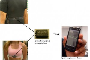
The system includes a series of nanostructured, textile sensors integrated into a conventional sports bra for women and vest for men. Via a lightweight and wireless module that snaps onto these garments, the sensors communicate with system software that relies on a smart phone to collect information, compress it and send it over a variety of wireless networks.

“Our e-bra enables continuous, real-time monitoring to identify any pathophysiological changes,” said Vijay Varadan, Distinguished Professor of electrical engineering. “It is a platform on which various sensors for cardiac-health monitoring are integrated into the fabric. The garment collects and transmits vital health signals to any desired location in the world.”

The system monitors blood pressure, body temperature, respiratory rate, oxygen consumption, some neural activity and all the readings provided by a conventional electrocardiograph (ECG), including the ability to display inverted T waves, which indicate the onset of cardiac arrest. The system does not require a cuff or any extra accessories to measure blood pressure and could therefore replace conventional blood-pressure monitors. It could also replace the cumbersome combination of ECG sensors and wires attached to patients while they walk on treadmills.

The researchers have provided this image,

The wireless monitoring system includes sensors, integrated into garments, that communicate health information to smart phones.

Here’s a bit more about the technology (from the May 3, 2012 news release),

The sensors, which are smaller than a dime, include gold nanowires, as well as flexible, conducting textile nanosensors. The sensors are made of arrays of gold nano-electrodes fabricated on a flexible substrate. The textile sensors are woven into the bra material. These sensors do not require conventional sticky electrodes or the use of gel.

Electrical signals and other physiological data gathered by the sensors are sent to the snap-on wireless module, the contents of which are housed in a plastic box that is slightly smaller than a ring box. As the critical wireless component, the module is essentially a low-powered laptop computer that includes an amplifier, an antenna, a printed circuit board, a microprocessor, a Bluetooth module, a battery and various sensors. The size of the module depends heavily on power consumption and minimum battery size. Varadan said that anticipated battery and Bluetooth upgrades will allow the researchers to build a smaller – 1.5 inches long, 0.75 inch wide and 0.25 inch deep – lighter and flexible module that will replace the rigid box.

Researchers are considering other applications for this technology (from the May 3, 2012 news release),

Data from the sensors then stream to commercially available cell phones and hand-held devices, which expand the use of the system beyond health care. By carrying a cell phone, athletes can monitor all signs mentioned above and other metrics, such as number of calories burned during a workout. To render clean data, the software includes filtering algorithms to mitigate problems due to motion of the hand-held device during exercise.

In light of the suggestion that this could be used by athletes I’m repeating my rhetorical question, have they thought about the sweat?

Thanks to Nanowerk where I first found out about this research at the University of Arkansas in their May 4, 2022 news item.


Majorana, matter, anti-matter, and nanowires

This is one of my favourite types of science story and I’m going to start with the quantum physics part of this (from the April 13, 2012 news item on Nanowerk),

Scientists at TU Delft’s Kavli Institute and the Foundation for Fundamental Research on Matter (FOM Foundation) have succeeded for the first time in detecting a Majorana particle. In the 1930s, the brilliant Italian physicist Ettore Majorana deduced from quantum theory the possibility of the existence of a very special particle, a particle that is its own anti-particle: the Majorana fermion. That ‘Majorana’ would be right on the border between matter and anti-matter.

The researchers have made a video about the Majorana fermion and nanowires (from the April 12, news release on the TU Delft website),

Here’s a little more about the Majorana fermion and why the researchers as so excited (from the TU Delft news release),

Majorana fermions are very interesting – not only because their discovery opens up a new and uncharted chapter of fundamental physics; they may also play a role in cosmology. A proposed theory assumes that the mysterious ‘dark matter, which forms the greatest part of the universe, is composed of Majorana fermions. Furthermore, scientists view the particles as fundamental building blocks for the quantum computer. Such a computer is far more powerful than the best supercomputer, but only exists in theory so far. Contrary to an ‘ordinary’ quantum computer, a quantum computer based on Majorana fermions is exceptionally stable and barely sensitive to external influences.

This breakthrough was achieved not with the Large Hadron Collider at CERN (European Particle Physics Laboratory) but with nanowires (from the TU Delft news release),

For the first time, scientists in Leo Kouwenhoven’s research group managed to create a nanoscale electronic device in which a pair of Majorana fermions ‘appear’ at either end of a nanowire. They did this by combining an extremely small nanowire, made by colleagues from Eindhoven University of Technology, with a superconducting material and a strong magnetic field. ‘The measurements of the particle at the ends of the nanowire cannot otherwise be explained than through the presence of a pair of Majorana fermions’, says Leo Kouwenhoven.

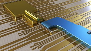
The device is made of an Indium Antemonide nanowire, covered with a Gold contact and partially covered with a Superconducting Niobium contact. The Majorana fermions are created at the end of the Nanowire. (from the TU Delft website)

At the end of the TU Delft news release, they mention more about Ettore Majorana and this is where the story gets quite intriguing,

The Italian physicist Ettore Majorana was a brilliant theorist who showed great insight into physics at a young age. He discovered a hitherto unknown solution to the equations from which quantum scientists deduce elementary particles: the Majorana fermion. Practically all theoretic particles that are predicted by quantum theory have been found in the last decades, with just a few exceptions, including the enigmatic Majorana particle and the well-known Higgs boson. But Ettore Majorana the person is every bit as mysterious as the particle. In 1938 he withdrew all his money and disappeared during a boat trip from Palermo to Naples. Whether he killed himself, was murdered or lived on under a different identity is still not known. No trace of Majorana was ever found.

Here’s the citation for the article describing the discovery of the Majorana fermion (from the TU Delft news release),

The article is published in Science Express on 12 April: Signatures of Majorana fermions in hybrid superconductor-semiconductor nanowire devices, V. Mourik, K. Zuo, S.M. Frolov, S.R. Plissard, E.P.A.M. Bakkers, L.P. Kouwenhoven

There’s more information and there are more images with the April 12, 2012 TU Deflt news release.

Nanowires, solar cells, McMaster University, Cleanfield Energy and partners

The Feb. 24, 2012 news item on Nanowerk offers an update on the solar cell project being undertaken by McMaster University (Ontario, Canada), Zhejiang University (China), Hyperion Shanghai Drive Technology Co. Ltd., and Cleanfield Energy (Ontario, Canada). From the news item,

[The four partners] were recently awarded an International Science and Technology Partnerships Program (ISTPP) grant, with an objective to further develop a new photovoltaic (PV) nanowire solar cell based on low cost substrates initially intended for the rapidly expanding concentrator photovoltaic (CPV) market.

The ISTPP funds will be used to develop a semiconductor nanowire, which will improve the efficiency and reduce fabrication costs of PV cells due to light trapping, enhanced carrier extraction, and the ability to use inexpensive substrates. This project will draw on the existing strengths of McMaster University in the fabrication of III-V compound semiconductor nanowires to advance the state-of-the-art PV and the Zhejiang University group, which have expertise in optoelectronic devices including electrode deposition and optical characterization of materials and devices.

For anyone who’s interested, here’s a description of the Canadian government’s International Science and Technology Partnerships Program (ISTPP), from their home page,

The International Science & Technology Partnerships Program (ISTPP) was announced by the Government of Canada in June 2005, to promote international collaborative research and development activities. The five-year, $20-million program will increase the international competitiveness and prosperity of Canada by building stronger science and technology relationships with Israel, India, China and Brazil. [emphasis mine]

The ISTPP will foster and support bilateral research projects which have the potential for commercialization between Canada and identified partner countries. It will also stimulate bilateral science and technology networking and matchmaking activities to further new partnerships and accelerate the commercialization of research and development. The ISTPP is a “seed fund”, meaning that various other public and private sector participants are also encouraged to bring S&T expertise and funds of their own to the bilateral relationship.

I see there’s no mention of Russia or South Africa, two members of a loose consortium of countries called the BRICS (Brazil, Russia, India, China, and South Africa).

Here are a few more technical details about the nanowires and solar cells from the news item,

The cost of PV devices can be reduced by replacing the single crystal substrates with thin film technology. However, the poly-crystalline nature of these thin film technologies generally results in reduced PV efficiency. To overcome these limitations, a substantial body of recent work in PV is beginning to exploit intentionally engineered nano-scale structures and the physics of reduced dimensionality to increase device performance. One of the leading contenders in the area of nanotechnology-based PV devices is semiconductor nanowires. .. Nanowires are easily grown using the well-known vapour-liquid-solid (VLS) process. The rapid growth rate (up to 10 microns per hour) and lower material utilization of nanowires compared to thin film PV devices implies lower fabrication costs. In addition, nanowires can be grown on less expensive substrates as compared to the expensive germanium substrates used in current concentrator PV cells.

The partners are hoping this project will lead to greater adoption of solar cells that are cheaper while maintaining their efficiency.

You can find out more about Cleanfield Energy here.

Nanowires in Turkey

Turkish researchers at Bilkent University in Ankara have recently discovered a means of reliably producing nanowires through a thermal size-reduction process that will be featured on the cover of Nature Materials July 2011 issue. From a June 17, 2011 news item in the Hürriyet Daily News (Istanbul),

A group of Turkish researchers at an Ankara university have manufactured the longest and thinnest nanowires ever produced, by employing a novel method to shrink matter 10-million fold.

The invention, discovered at Bilkent University’s National Nanotechnology Research Center, or UNAM, is set to appear on the cover of Nature Material magazine’s July edition.

“At this moment, we may not even be able to predict what things will be produced [in the future] using this method,” said Associate Professor Mehmet Bayýndýr who led the research team.

The research team was trying to obtain a patent for their invention, as well as preparing to apply to the Guinness Book of Records for producing the world’s longest and thinnest semiconductor nanowire.

Here’s a little more information about nanowires and some detail about the thermal-size reduction process from the study in Nature Materials’ (full article is behind a paywall) online publication,

Nanowires are arguably the most studied nanomaterial model to make functional devices and arrays. … Here we report a new thermal size-reduction process to produce well-ordered, globally oriented, indefinitely long nanowire and nanotube arrays with different materials. The new technique involves iterative co-drawing of hermetically sealed multimaterials in compatible polymer matrices similar to fibre drawing. Globally oriented, endlessly parallel, axially and radially uniform semiconducting and piezoelectric nanowire and nanotube arrays hundreds of metres long, with nanowire diameters less than 15 nm, are obtained. The resulting nanostructures are sealed inside a flexible substrate, facilitating the handling of and electrical contacting to the nanowires. Inexpensive, high-throughput, multimaterial nanowire arrays pave the way for applications including nanowire-based large-area flexible sensor platforms, phase-changememory, nanostructure-enhanced photovoltaics, semiconductor nanophotonics, dielectric metamaterials,linear and nonlinear photonics and nanowire-enabled high-performance composites.

For interested parties, here’s the citation:

Arrays of indefinitely long uniform nanowires and nanotubes by Mecit Yaman, Tural Khudiyev, Erol Ozur, Mehmet Kanik, Ozan Aktas, Ekin O. Ozgur, Hakan Deniz, Enes Korkut, and Mehmet Bayindir. Nature Materials July 2011. Published online June 12, 2011. doi:10.1038/nmat3038


Nanotechnology-enabled robot skin

We take it for granted most of the time. The ability to sense pressure and respond to appropriately doesn’t seem like any great gift but without it, you’d crush fragile objects or be unable to hold onto the heavy ones.

It’s this ability to sense pressure that’s a stumbling block for robotmakers who want to move robots into jobs that require some dexterity, e.g., one that could clean yours windows and your walls without damaging one or failing to clean the other.

Two research teams have recently published papers about their work on solving the ‘pressure problem’. From the article by Jason Palmer for BBC News,

The materials, which can sense pressure as sensitively and quickly as human skin, have been outlined by two groups reporting in [the journal] Nature Materials.

The skins are arrays of small pressure sensors that convert tiny changes in pressure into electrical signals.

The arrays are built into or under flexible rubber sheets that could be stretched into a variety of shapes.

The materials could be used to sheath artificial limbs or to create robots that can pick up and hold fragile objects. They could also be used to improve tools for minimally-invasive surgery.

One team is located at the University of California, Berkeley and the other at Stanford University. The Berkeley team headed by Ali Javey, associate professor of electrical engineering and computer sciences has named their artificial skin ‘e-skin’. From the article by Dan Nosowitz on the Fast Company website,

Researchers at the University of California at Berkeley, backed by DARPA funding, have come up with a thin prototype material that’s getting science nerds all in a tizzy about the future of robotics.

This material is made from germanium and silicon nanowires grown on a cylinder, then rolled around a sticky polyimide substrate. What does that get you? As CNet says, “The result was a shiny, thin, and flexible electronic material organized into a matrix of transistors, each of which with hundreds of semiconductor nanowires.”

But what takes the material to the next level is the thin layer of pressure-sensitive rubber added to the prototype’s surface, capable of measuring pressures between zero and 15 kilopascals–about the normal range of pressure for a low-intensity human activity, like, say, writing a blog post. Basically, this rubber layer turns the nanowire material into a sort of artificial skin, which is being played up as a miracle material.

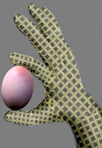
As Nosowitz points out, this is a remarkable achievement and it is a first step since skin registers pressure, pain, temperature, wetness, and more. Here’s an illustration of Berkeley’s e-skin (Source: University of California Berkeley, accessed from  http://berkeley.edu/news/media/releases/2010/09/12_eskin.shtml Sept. 14, 2010),

An artist’s illustration of an artificial e-skin with nanowire active matrix circuitry covering a hand. The fragile egg illustrates the functionality of the e-skin device for prosthetic and robotic applications.

The Stanford team’s approach has some similarities to the Berkeley’s (from Jason Palmer’s BBC article),

“Javey’s work is a nice demonstration of their capability in making a large array of nanowire TFTs [this film transistor],” said Zhenan Bao of Stanford University, whose group demonstrated the second approach.

The heart of Professor Bao’s devices is micro-structured rubber sheet in the middle of the TFT – effectively re-creating the functionality of the Berkeley group’s skins with less layers.

“Instead of laminating a pressure-sensitive resistor array on top of a nanowire TFT array, we made our transistors to be pressure sensitive,” Professor Bao explained to BBC News.

Here’s a short video about the Stanford team’s work (Source: Stanford University, accessed from http://news.stanford.edu/news/2010/september/sensitive-artificial-skin-091210.html Sept. 14, 2010),

Both approaches to the ‘pressure problem’ have at least one shortcoming. The Berkeley’s team’s e-skin has less sensitivity than Stanford’s while the Stanford team’s artificial skin is less flexible than e-skin as per Palmer’s BBC article. Also, I noticed that the Berkeley team at least is being funded by DARPA ([US Dept. of Defense] Defense Advanced Research Projects Agency) so I’m assuming a fair degree of military interest, which always gives me pause. Nonetheless, bravo to both teams.

Nanotechnology and biocompatibility; carbon nanotubes in agriculture; venture capital for nanotechnology

One of the big nanotechnology toxicity issues centers around the question of its biocompatibility i.e. what effect do the particles have on cells in human bodies, plants, and other biological organisms? Right now, the results are mixed. Two studies have recently been published which suggest that there are neutral or even positive responses to nanoparticles.

Researchers at Lund University (Sweden) have conducted tests of nanowires, which they are hoping could be used as electrodes in the future, showing that microglial cells break down the nanowires and almost completely clean them away over a period of weeks. You can read more about the work here on Nanowerk. I would expect they’ll need to do more studies confirming these results as well more tests establishing what happens to the nanowire debris over longer periods of time and what problems, if any, emerge when electrodes are introduced in succession (i.e. how many times can you implant nanowires and have them ‘mostly’ cleaned away?).

The other biocompatibility story centers on food stuffs. Apparently carbon nanotubes can have a positive effect on crops. According to researchers in Arkansas*, Mariya Khodakovskaya, Alexandru Biris, and their colleagues, the treated seeds (tomato) sprouted twice as fast and grew more than twice as much as their untreated neighbours. The news item is here on Nanowerk and there is a more in-depth article about agriculture and nanotechnology here in Nanowerk Spotlight. (Note: I have checked and both of the papers have been published although I believe they’re both behind paywalls.)

It seems be to a Nanowerk day as I’m featuring the site again for this item. They have made a guide to finding venture capital for startup nanotechnology companies available on their site. From the item,

To help potential nanotechnology start-up founders with shaping their plans, Nanowerk, the leading nanotechnology information service, and Nanostart, the world’s leading nanotechnology venture capital company, have teamed up to provide this useful guide which particularly addresses the funding aspects of nanotechnology start-ups, along with answers to some of the most commonly asked questions.

You can read more here.

*’Arkansaa’ corrected to ‘Arkansas’ on Dec. 7, 2017.

More titanium dioxide news; the 5th anniversary of the Royal Society’s Report on Nanotechnology; Copyright in Canada

While titanium dioxide particles in sunscreens are considered safe (see my blog posting here), there is a new study which suggests concerns. A study was done in Japan on pregnant mice who were injected with titanium dioxide nanoparticles. The results suggest that the particles affected brain development in the foetuses. (The media release is located at Nanowerk News here.) My questions since I haven’t looked at the study are this:  Where was the injection site? What was the concentration of  titanium dioxide nanoparticles in the solution? Where several concentrations used or only one? (After all, a lot of medicines are poison if taken in the wrong dosage or misapplied [taken internally instead of externally].)

Still on the titanium dioxide trail, there’s a study by researchers in Switzerland which suggests that nanowires and nanotubes made of titanium dixoide are toxic. There’s an article by Miichael Berger here on Nanowerks. From Berger’s article,

One of the complications of nanotoxicology is that the toxicity of a specific nanomaterial cannot be predicted from the toxicity of the same material in a different form.

“TiO2 nanoparticles are widely used as UV blockers in sunscreens” says Arnaud Magrez [researcher]. “Their cytotoxicity has been tested before and they were found to be rather non-toxic. Our new study shows that TiO2 based nanofilaments, however, can be quite toxic. The geometry of nanoparticles appears to play a crucial role in cytotoxicity. Furthermore, the toxicity can be enhanced by the presence of defects on the nanofilament surface, resulting from chemical treatment.”

Both of these studies highlight why more research needs to be done. A comment which is made in an entirely different context by Dr. Andrew Maynard in his essay commemorating the anniversary of the Royal Society/Royal Academy of Engineering 2004 report on nanotechnologies. Maynard’s essay is the foreword to a report, 5 years on – a beacon or just a landmark? Reflections on the 2004  Royal Society/Royal Academy of Engineering report into nanotechnologies – what was its impact and what is its legacy? published by the Responsible Nano Forum. Maynard’s essay can be read here on his 2020 Science blog and the report can be found here. From Maynard’s essay,

At the time, concerns were mounting over possible new risks associated with creating materials and devices at the nanoscale, and how these would affect the technology’s development.  The previous year, Michael Crichton’s book Prey had sent the nanotech community into a tizzy over a speculative public backlash against the emerging science and technology.  And researchers were beginning to reveal hints that novel nanoscale materials could also affect humans and the environment in unconventional ways—getting to places and causing harm on a scale that belied their small size.

Do read it if you have the time. Maynard’s perspective is both historical and contemporary.

And now for something which concerns me when writing this blog, copyright. Since this blog isn’t profitmaking and I give attribution and encourage people to visit the sites and blogs I quote from, I’ve considered what I do ‘fair use’. If you’ve been following the copyright discussion, you know ‘fair use’ is being debated fiercely as is intellectual property law which includes copyright, patents, and trademarks.

After a rather disastrous attempt to introduce new copyright legislation (last fall I think), the Canadian government has launched a public consultation process. (I too was surprised to find out about it.) The roundtable meeting in Vancouver took place about 10 days ago. There will be roundtable meetings  elsewhere and two town hall meetings (where the public will be invited). If you’re a member of the public who’s lucky enough to live in either Toronto or Montreal, you can have your say in real time. The rest of us can participate online here at the Copyright Counsultations website. You do have to register to participate. The Vancouver roundtable meeting has been transcribed and is available online here and the trasncript for the Calgary roundtable is here.