Tag Archives: U.S. Department of Energy

Nanoparticle snapshots with femtosecond photography

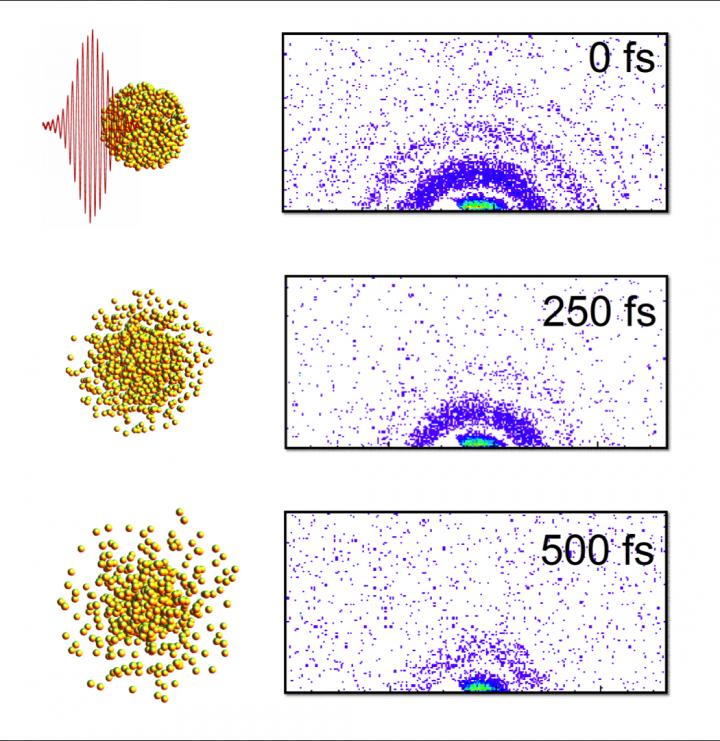
Caption: Here are "stills" from an X-ray "movie" of an exploding nanoparticle. The nanoparticle is superheated with an intense optical pulse and subsequently explodes (left). A series of ultrafast x-ray diffraction images (right) maps the process and contains information how the explosion starts with surface softening and proceeds from the outside in. Credit: Christoph Bostedt

Caption: Here are “stills” from an X-ray “movie” of an exploding nanoparticle. The nanoparticle is superheated with an intense optical pulse and subsequently explodes (left). A series of ultrafast x-ray diffraction images (right) maps the process and contains information how the explosion starts with surface softening and proceeds from the outside in. Credit: Christoph Bostedt

A Feb. 10, 2016 news item on Nanotechnology Now provides more information about the ‘snapshots,

Just as a photographer needs a camera with a split-second shutter speed to capture rapid motion, scientists looking at the behavior of tiny materials need special instruments with the capacity to see changes that happen in the blink of an eye.

An international team of researchers led by X-ray scientist Christoph Bostedt of the U.S. Department of Energy’s (DOE) Argonne National Laboratory and Tais Gorkhover of DOE’s SLAC National Accelerator Laboratory used two special lasers to observe the dynamics of a small sample of xenon as it was heated to a plasma.

A Feb. 10, 2016 Argonne National Laboratory news release (also on EurekAlert) by Jared Sagoff, which originated the news item, provides more technical details,

Bostedt and Gorkhover were able to use the Linac Coherent Light Source (LCLS) at SLAC to make observations of the sample in time steps of approximately a hundred femtoseconds – a femtosecond being one millionth of a billionth of a second [emphasis mine]. The exposure time of the individual images was so short that the quickly moving particles in the gas phase appeared frozen. “The advantage of a machine like the LCLS is that it gives us the equivalent of high-speed flash photography as opposed to a pinhole camera,” Bostedt said. The LCLS is a DOE Office of Science User Facility.

The researchers used an optical laser to heat the sample cluster and an X-ray laser to probe the dynamics of the cluster as it changed over time. As the laser heated the cluster, the photons freed electrons initially bound to the atoms; however, these electrons still remained loosely bound to the cluster.

By imaging exploding nanoparticles, the team was able to make measurements of how they change over time in extreme environments. “Ultimately, we want to understand how the energy from the light affects the system,” Gorkhover said.

“There are really no other techniques that give us this good a resolution in both time and space simultaneously,” she added. “Other methods require us to take averages over many different ‘exposures,’ which can obscure relevant details. Additionally, techniques like electron microscopy involve a substrate material that can interfere with the behavior of the sample.”

According to Bostedt, the research could also impact the study of aerosols in the environment or in combustion, as the dual-laser “pump and probe” model could be adapted to study materials in the gas phase. “Although our material goes from solid to plasma very quickly, there are other types of materials you could study with this or a similar technique,” he said.

I marvel at how very brief the time intervals are at the femtoscale and for that matter, the other subatomic scales.

Here’s a link to and a citation for the paper,

Femtosecond and nanometre visualization of structural dynamics in superheated nanoparticles by Tais Gorkhover, Sebastian Schorb, Ryan Coffee, Marcus Adolph, Lutz Foucar, Daniela Rupp, Andrew Aquila, John D. Bozek, Sascha W. Epp, Benjamin Erk, Lars Gumprecht, Lotte Holmegaard, Andreas Hartmann, Robert Hartmann, Günter Hauser, Peter Holl, Andre Hömke, Per Johnsson, Nils Kimmel, Kai-Uwe Kühnel, Marc Messerschmidt, Christian Reich, Arnaud Rouzée, Benedikt Rudek, Carlo Schmidt et al. Nature Photonics 10, 93–97 (2016) doi:10.1038/nphoton.2015.264 Published online 25 January 2016

This paper is behind a paywall.

Combining optical technology with nanocomposite films at Oregon State University (OSU)

There is a lot of pressure in the US to commercialize nanotechnology-enabled products—a perfectly understandable stance after investing over $22B since 2000. Engineers at Oregon State University (OSU) are hoping to attract industry partners to improve and commercialize their gas sensors (from an April 2, 2015 OSU news release also on EurekAlert),

Engineers have combined innovative optical technology with nanocomposite thin-films to create a new type of sensor that is inexpensive, fast, highly sensitive and able to detect and analyze a wide range of gases.

The technology might find applications in everything from environmental monitoring to airport security or testing blood alcohol levels. The sensor is particularly suited to detecting carbon dioxide, and may be useful in industrial applications or systems designed to store carbon dioxide underground, as one approach to greenhouse gas reduction.

Oregon State University has filed for a patent on the invention, developed in collaboration with scientists at the National Energy Technology Lab or the U.S. Department of Energy, and with support from that agency. The findings were just reported in the Journal of Materials Chemistry C.

University researchers are now seeking industrial collaborators to further perfect and help commercialize the system.

“Optical sensing is very effective in sensing and identifying trace-level gases, but often uses large laboratory devices that are terribly expensive and can’t be transported into the field,” said Alan Wang, a photonics expert and an assistant professor in the OSU School of Electrical Engineering and Computer Science.

“By contrast, we use optical approaches that can be small, portable and inexpensive,” Wang said. “This system used plasmonic nanocrystals that act somewhat like a tiny lens, to concentrate a light wave and increase sensitivity.”

This approach is combined with a metal-organic framework of thin films, which can rapidly adsorb gases within material pores, and be recycled by simple vacuum processes. After the thin film captures the gas molecules near the surface, the plasmonic materials act at a near-infrared range, help magnify the signal and precisely analyze the presence and amounts of different gases.

“By working at the near-infrared range and using these plasmonic nanocrystals, there’s an order of magnitude increase in sensitivity,” said Chih-hung Chang, an OSU professor of chemical engineering. “This type of sensor should be able to quickly tell exactly what gases are present and in what amount.”

That speed, precision, portability and low cost, the researchers said, should allow instruments that can be used in the field for many purposes. The food industry, for industry, uses carbon dioxide in storage of fruits and vegetables, and the gas has to be kept at certain levels.

Gas detection can be valuable in finding explosives, and new technologies such as this might find application in airport or border security. Various gases need to be monitored in environmental research, and there may be other uses in health care, optimal function of automobile engines, and prevention of natural gas leakage.

The paper can be found here,

Plasmonics-enhanced metal–organic framework nanoporous films for highly sensitive near-infrared absorption by Ki-Joong Kim, Xinyuan Chong, Peter B. Kreider, Guoheng Ma,  Paul R. Ohodnicki, John P. Baltrus, Alan X. Wang, and Chih-Hung Chang. J. Mater. Chem. C, 2015,3, 2763-2767 DOI: 10.1039/C4TC02846E First published online 09 Feb 2015

It is behind a paywall.

Buckydiamondoids steer electron flow

One doesn’t usually think about buckyballs (Buckminsterfullerenes) and diamondoids as being together in one molecule but that has not stopped scientists from trying to join them and, in this case, successfully. From a Sept. 9, 2014 news item on ScienceDaily,

Scientists have married two unconventional forms of carbon — one shaped like a soccer ball, the other a tiny diamond — to make a molecule that conducts electricity in only one direction. This tiny electronic component, known as a rectifier, could play a key role in shrinking chip components down to the size of molecules to enable faster, more powerful devices.

Here’s an illustration the scientists have provided,

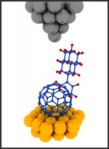
Illustration of a buckydiamondoid molecule under a scanning tunneling microscope (STM). In this study the STM made images of the buckydiamondoids and probed their electronic properties.

Illustration of a buckydiamondoid molecule under a scanning tunneling microscope (STM). In this study the STM made images of the buckydiamondoids and probed their electronic properties.

A Sept. 9, 2014 Stanford University news release by Glenda Chui (also on EurekAlert), which originated the news item, provides some information about this piece of international research along with background information on buckyballs and diamondoids (Note: Links have been removed),

“We wanted to see what new, emergent properties might come out when you put these two ingredients together to create a ‘buckydiamondoid,'” said Hari Manoharan of the Stanford Institute for Materials and Energy Sciences (SIMES) at the U.S. Department of Energy’s SLAC National Accelerator Laboratory. “What we got was basically a one-way valve for conducting electricity – clearly more than the sum of its parts.”

The research team, which included scientists from Stanford University, Belgium, Germany and Ukraine, reported its results Sept. 9 in Nature Communications.

Many electronic circuits have three basic components: a material that conducts electrons; rectifiers, which commonly take the form of diodes, to steer that flow in a single direction; and transistors to switch the flow on and off. Scientists combined two offbeat ingredients – buckyballs and diamondoids – to create the new diode-like component.

Buckyballs – short for buckminsterfullerenes – are hollow carbon spheres whose 1985 discovery earned three scientists a Nobel Prize in chemistry. Diamondoids are tiny linked cages of carbon joined, or bonded, as they are in diamonds, with hydrogen atoms linked to the surface, but weighing less than a billionth of a billionth of a carat. Both are subjects of a lot of research aimed at understanding their properties and finding ways to use them.

In 2007, a team led by researchers from SLAC and Stanford discovered that a single layer of diamondoids on a metal surface can emit and focus electrons into a tiny beam. Manoharan and his colleagues wondered: What would happen if they paired an electron-emitting diamondoid with another molecule that likes to grab electrons? Buckyballs are just that sort of electron-grabbing molecule.

Details are then provided about this specific piece of research (from the Stanford news release),

For this study, diamondoids were produced in the SLAC laboratory of SIMES researchers Jeremy Dahl and Robert Carlson, who are world experts in extracting the tiny diamonds from petroleum. The diamondoids were then shipped to Germany, where chemists at Justus-Liebig University figured out how to attach them to buckyballs.

The resulting buckydiamondoids, which are just a few nanometers long, were tested in SIMES laboratories at Stanford. A team led by graduate student Jason Randel and postdoctoral researcher Francis Niestemski used a scanning tunneling microscope to make images of the hybrid molecules and measure their electronic behavior. They discovered that the hybrid is an excellent rectifier: The electrical current flowing through the molecule was up to 50 times stronger in one direction, from electron-spitting diamondoid to electron-catching buckyball, than in the opposite direction. This is something neither component can do on its own.

While this is not the first molecular rectifier ever invented, it’s the first one made from just carbon and hydrogen, a simplicity researchers find appealing, said Manoharan, who is an associate professor of physics at Stanford. The next step, he said, is to see if transistors can be constructed from the same basic ingredients.

“Buckyballs are easy to make – they can be isolated from soot – and the type of diamondoid we used here, which consists of two tiny cages, can be purchased commercially,” he said. “And now that our colleagues in Germany have figured out how to bind them together, others can follow the recipe. So while our research was aimed at gaining fundamental insights about a novel hybrid molecule, it could lead to advances that help make molecular electronics a reality.”

Other research collaborators came from the Catholic University of Louvain in Belgium and Kiev Polytechnic Institute in Ukraine. The primary funding for the work came from U.S. the Department of Energy Office of Science (Basic Energy Sciences, Materials Sciences and Engineering Divisions).

Here’s a link to and a citation for the paper,

Unconventional molecule-resolved current rectification in diamondoid–fullerene hybrids by Jason C. Randel, Francis C. Niestemski,    Andrés R. Botello-Mendez, Warren Mar, Georges Ndabashimiye, Sorin Melinte, Jeremy E. P. Dahl, Robert M. K. Carlson, Ekaterina D. Butova, Andrey A. Fokin, Peter R. Schreiner, Jean-Christophe Charlier & Hari C. Manoharan. Nature Communications 5, Article number: 4877 doi:10.1038/ncomms5877 Published 09 September 2014

This paper is open access. The scientists provided not only a standard illustration but a pretty picture of the buckydiamondoid,

Caption: An international team led by researchers at SLAC National Accelerator Laboratory and Stanford University joined two offbeat carbon molecules -- diamondoids, the square cages at left, and buckyballs, the soccer-ball shapes at right -- to create "buckydiamondoids," center. These hybrid molecules function as rectifiers, conducting electrons in only one direction, and could help pave the way to molecular electronic devices. Credit: Manoharan Lab/Stanford University

Caption: An international team led by researchers at SLAC National Accelerator Laboratory and Stanford University joined two offbeat carbon molecules — diamondoids, the square cages at left, and buckyballs, the soccer-ball shapes at right — to create “buckydiamondoids,” center. These hybrid molecules function as rectifiers, conducting electrons in only one direction, and could help pave the way to molecular electronic devices.
Credit: Manoharan Lab/Stanford University

Mining uranium from the ocean

We are running short of uranium as terrestrial mining of this element has become more hazardous environmentally. A July 18, 2014 news item on Azonano highlights an ‘ocean mining’ uranium project at the University of Alabama (US),

The U.S. Department of Energy [DOE] selected a University of Alabama [UA] start-up company for an approximate $1.5 million award to refine an alternative material to potentially extract uranium from the ocean.

Uranium, which naturally occurs in seawater and in the Earth’s crust, is the fuel for nuclear power. For decades, scientists have sought a more economical and efficient way to remove it from the ocean, as the terrestrial supply is dwindling and environmentally unfriendly to mine.

A July 17, 2014 University of Alabama news release, which originated the news item, describe the University of Alabama’s unique approach to the problem of extracting uranium from the ocean (Note: A link has been removed),

“Every scientist in the world, except us, who is trying to do this is working with plastics,” said Dr. Gabriela Gurau, a chemist and CEO of the UA-based company, 525 Solutions.

Instead, the UA company is developing an adsorbent, biodegradable material made from the compound chitin, which is found in shrimp shells and in other crustaceans and insects. The researchers have developed transparent sheets, or mats, comprised of tiny chitin fibers, modified for the task. When suspended beneath the ocean’s surface, the mats are designed to withdraw uranium.

“Once you put it in the ocean, it will attract uranium like a magnet, and uranium will stick to it,” said Gurau, a University of Alabama alumna.

If one day implemented, the mats, with uranium attached, would be taken to an industrial plant where the nuclear fuel source would be removed.

Earlier work led by Dr. Robin Rogers, Robert Ramsay Chair of Chemistry at UA and director of UA’s Center for Green Manufacturing, initially proved the concept for extracting uranium using chitin. Rogers is an owner/founder of 525 Solutions and serves as a scientific adviser to the company’s representatives.

“The oceans are estimated to contain more than a thousand times the amount of uranium found in total in any known land deposit,” Rogers said. “Fortunately, the concentration of uranium in the ocean is very, very low, but the volume of the oceans is, of course, very, very high. Assuming we could recover only half of this resource, this much uranium could support 6,500 years of nuclear capacity.”

Removing chitin, in a pure form, from shells had previously proven difficult, but Rogers and his UA colleagues discovered a way to use a relatively new class of solvents, called ionic liquids, for removal. Ionic liquids are liquid salts which have other unique and desirable properties that traditional solvents do not. Rogers is recognized as a world-leader in the field of  ionic liquids.

UA researchers use a time-honored laboratory technique called electrospinning to produce the mats. In this process, the scientists use a specially-prepared, chitin-based, ionic liquid solution, which is loaded in the electrospinning apparatus. Some 30,000 volts of electricity are applied, spinning the fibers into a water bath. After several hours, nanofiber mats, consisting of fibers much thinner than a strand of a spider’s web, form, weaved together into a solid sheet.

The increased surface area the nanomats provide is central to the project, said Dr. Julia Shamshina, the company’s chief technology officer and also a UA alumna.

“The larger the surface area, the larger modifications we can make and the more uranium it will uptake,” Shamshina said. “If you have one very thick fiber and 10 which, when combined, equal the size of the thick fiber, the ten smaller ones will take up hundreds, or even thousands, of times more uranium.”

Rogers extolled the potential environmental benefits of  the company’s approach and addressed cost factors.

“Mining uranium from land is a very dirty, energy intensive process, with a lot of hazardous waste produced,” Rogers said. “If we eliminate land mining by mining from the ocean, we not only clean up the ocean, we eliminate all of the environmental problems with terrestrial mining.

“Research studies have shown that uranium can be extracted from the ocean, but the process remains prohibitively costly,” said Rogers, a  two-time UA graduate. “The search for more effective adsorbents — which is what we’re doing  – is under way and expected to solve this issue.”

Gurau said the two-year grant, from the DOE’s Office of Science through its Small Business Innovation Research and Small Business Technology Transfer programs, will enable the researchers to refine their processes, measure costs and conduct an environmental analysis.

“We need to know if it’s viable from an economic standpoint,” Gurau said. “I think this is a critical step in getting this to the pilot-plant stage.”

Cooling it—an application using carbon nanotubes and a theory that hotter leads to cooler

The only thing these two news items have in common is their focus on cooling down electronic devices. Well, there’s also the fact that the work is being done at the nanoscale.

First, there’s a Jan. 23, 2014 news item on Azonano about a technique using carbon nanotubes to cool down microprocessors,

“Cool it!” That’s a prime directive for microprocessor chips and a promising new solution to meeting this imperative is in the offing. Researchers with the U.S. Department of Energy (DOE)’s Lawrence Berkeley National Laboratory (Berkeley Lab) have developed a “process friendly” technique that would enable the cooling of microprocessor chips through carbon nanotubes.

Frank Ogletree, a physicist with Berkeley Lab’s Materials Sciences Division, led a study in which organic molecules were used to form strong covalent bonds between carbon nanotubes and metal surfaces. This improved by six-fold the flow of heat from the metal to the carbon nanotubes, paving the way for faster, more efficient cooling of computer chips. The technique is done through gas vapor or liquid chemistry at low temperatures, making it suitable for the manufacturing of computer chips.

The Jan. 22, 2014 Berkeley Lab news release (also on EurekAlert), which originated the news item, describes the nature  of the problem in more detail,

Overheating is the bane of microprocessors. As transistors heat up, their performance can deteriorate to the point where they no longer function as transistors. With microprocessor chips becoming more densely packed and processing speeds continuing to increase, the overheating problem looms ever larger. The first challenge is to conduct heat out of the chip and onto the circuit board where fans and other techniques can be used for cooling. Carbon nanotubes have demonstrated exceptionally high thermal conductivity but their use for cooling microprocessor chips and other devices has been hampered by high thermal interface resistances in nanostructured systems.

“The thermal conductivity of carbon nanotubes exceeds that of diamond or any other natural material but because carbon nanotubes are so chemically stable, their chemical interactions with most other materials are relatively weak, which makes for  high thermal interface resistance,” Ogletree says. “Intel came to the Molecular Foundry wanting to improve the performance of carbon nanotubes in devices. Working with Nachiket Raravikar and Ravi Prasher, who were both Intel engineers when the project was initiated, we were able to increase and strengthen the contact between carbon nanotubes and the surfaces of other materials. This reduces thermal resistance and substantially improves heat transport efficiency.”

The news release then describes the proposed solution,

Sumanjeet Kaur, lead author of the Nature Communications paper and an expert on carbon nanotubes, with assistance from co-author and Molecular Foundry chemist Brett Helms, used reactive molecules to bridge the carbon nanotube/metal interface – aminopropyl-trialkoxy-silane (APS) for oxide-forming metals, and cysteamine for noble metals. First vertically aligned carbon nanotube arrays were grown on silicon wafers, and thin films of aluminum or gold were evaporated on glass microscope cover slips. The metal films were then “functionalized” and allowed to bond with the carbon nanotube arrays. Enhanced heat flow was confirmed using a characterization technique developed by Ogletree that allows for interface-specific measurements of heat transport.

“You can think of interface resistance in steady-state heat flow as being an extra amount of distance the heat has to flow through the material,” Kaur says. “With carbon nanotubes, thermal interface resistance adds something like 40 microns of distance on each side of the actual carbon nanotube layer. With our technique, we’re able to decrease the interface resistance so that the extra distance is around seven microns at each interface.”

Although the approach used by Ogletree, Kaur and their colleagues substantially strengthened the contact between a metal and individual carbon nanotubes within an array, a majority of the nanotubes within the array may still fail to connect with the metal. The Berkeley team is now developing a way to improve the density of carbon nanotube/metal contacts. Their technique should also be applicable to single and multi-layer graphene devices, which face the same cooling issues.

For anyone who’s never heard of the Molecular Foundry before (from the news release),

The Molecular Foundry is one of five DOE [Department of Energy] Nanoscale Science Research Centers (NSRCs), national user facilities for interdisciplinary research at the nanoscale, supported by the DOE Office of Science. Together the NSRCs comprise a suite of complementary facilities that provide researchers with state-of-the-art capabilities to fabricate, process, characterize, and model nanoscale materials, and constitute the largest infrastructure investment of the National Nanotechnology Initiative. The NSRCs are located at DOE’s Argonne, Brookhaven, Lawrence Berkeley, Oak Ridge and Sandia and Los Alamos national laboratories.

My second item comes from the University of Buffalo (UB), located in the US. From a Jan. 21, 2014 University of Buffalo news release by Cory Nealon (also on EurekAlert),

Heat in electronic devices is generated by the movement of electrons through transistors, resistors and other elements of an electrical network. Depending on the network, there are a variety of ways, such as cooling fans and heat sinks, to prevent the circuits from overheating.

But as more integrated circuits and transistors are added to devices to boost their computing power, it’s becoming more difficult to keep those elements cool. Most nanoelectrics research centers are working to develop advanced materials that are capable of withstanding the extreme environment inside smartphones, laptops and other devices.

While advanced materials show tremendous potential, the UB research suggests there may still be room within the existing paradigm of electronic devices to continue developing more powerful computers.

To support their findings, the researchers fabricated nanoscale semiconductor devices in a state-of-the-art gallium arsenide crystal provided to UB by Sandia’s Reno [John L. Reno, Center for Integrated Nanotechnologies at Sandia National Laboratories]. The researchers then subjected the chip to a large voltage, squeezing an electrical current through the nanoconductors. This, in turn, increased the amount of heat circulating through the chip’s nanotransistor.

But instead of degrading the device, the nanotransistor spontaneously transformed itself into a quantum state that was protected from the effect of heating and provided a robust channel of electric current. To help explain, Bird [Jonathan Bird, UB professor of electrical engineering] offered an analogy to Niagara Falls.

“The water, or energy, comes from a source; in this case, the Great Lakes. It’s channeled into a narrow point (the Niagara River) and ultimately flows over Niagara Falls. At the bottom of waterfall is dissipated energy. But unlike the waterfall, this dissipated energy recirculates throughout the chip and changes how heat affects, or in this case doesn’t affect, the network’s operation.”

While this behavior may seem unusual, especially conceptualizing it in terms of water flowing over a waterfall, it is the direct result of the quantum mechanical nature of electronics when viewed on the nanoscale. The current is made up of electrons which spontaneously organize to form a narrow conducting filament through the nanoconductor. It is this filament that is so robust against the effects of heating.

“We’re not actually eliminating the heat, but we’ve managed to stop it from affecting the electrical network. In a way, this is an optimization of the current paradigm,” said Han [J. E. Han, UB Dept. of Physics], who developed the theoretical models which explain the findings.

What an interesting and counter-intuitive approach to managing the heat in our devices.

For those who want more, here’s a link to and citation for the carbon nanotube paper,

Enhanced thermal transport at covalently functionalized carbon nanotube array interfaces by Sumanjeet Kaur, Nachiket Raravikar, Brett A. Helms, Ravi Prasher, & D. Frank Ogletree. Nature Communications 5, Article number: 3082 doi:10.1038/ncomms4082 Published 22 January 2014

This paper is behind a paywall.

Now here’s a link to and a citation for the ‘making it hotter to make it cooler’ paper,

Formation of a protected sub-band for conduction in quantum point contacts under extreme biasing by J. Lee, J. E. Han, S. Xiao, J. Song, J. L. Reno, & J. P. Bird. Nature Nanotechnology (2014) doi:10.1038/nnano.2013.297 Published online 19 January 2014

This paper is behind a paywall although there is an option to preview it for free via ReadCube Access.

Combining bacteriorhodopsin with semiconducting nanoparticles to generate hydrogen

Scientists at the US Argonne National Laboratory have created a hybrid bio-assisted photocatalyst according to a July 19, 2013 news item on ScienceDaily,

A protein found in the membranes of ancient microorganisms that live in desert salt flats could offer a new way of using sunlight to generate environmentally friendly hydrogen fuel, according to a new study by researchers at the U.S. Department of Energy’s Argonne National Laboratory.

Argonne nanoscientist Elena Rozhkova and her colleagues combined a pigment called bacteriorhodopsin with semiconducting nanoparticles to create a system that uses light to spark a catalytic process that creates hydrogen fuel.

Before getting to the new hybrid the story starts with nano titanium dioxide (from the July 16, 2013 Argonne National Laboratory press release, which originated the news item),

Scientists have been aware of the potential of titanium dioxide nanoparticles for light-based reactions since the early 1970s, when Japanese researchers discovered that a titanium dioxide electrode exposed to bright ultraviolet light could split water molecules in a phenomenon that came to be known as the Honda-Fujishima effect. Since then, scientists have made continuous efforts to extend the light reactivity of titanium dioxide photocatalysts into the visible part of the spectrum. The promise of these photocatalysts prompted scientists to experiment with different modifications to their basic chemistry in hope of making the reaction more efficient, Rozhkova said.

“Titanium dioxide alone reacts with ultraviolet light, but not with visible light, so we used biological photoreactive molecules as a building block to create a hybrid system that could use visible light efficiently,” Rozhkova said.

Rozhkova and her colleagues turned to bacteriorhodopsin – which is responsible for the unusual purple color of a number of salt flats in California and Nevada – because it uses sunlight as an energy source that allows it to act as a “proton pump.”  Proton pumps are proteins that typically straddle a cellular membrane and transfer protons from inside the cell to the extracellular space.

Here’s an image of the purple membrane caused by bacteriorhodopsin (from University of Bari [Italy] Professor Angela Correlli’s webpage of Photorecptors and Olfactory Receptors,

Bacteriorhodopsin is the only protein of purple membranes, which contains few different lipids. [downloaded from the University of Bari: http://www.biologia.uniba.it/fisiologia/corcelli/en/ric2.html]

Bacteriorhodopsin is the only protein of purple membranes, which contains few different lipids. [downloaded from the University of Bari: http://www.biologia.uniba.it/fisiologia/corcelli/en/ric2.html]

The press release goes on to describe the hybrid system,

In the Argonne system, the protons provided by the bacteriorhodopsin are combined with free electrons at small platinum sites interspersed in the titanium dioxide matrix. “The platinum nanoparticles are essential for creating a distinct spot for the production of the hydrogen molecule,” said Peng Wang, an Argonne postdoctoral researcher in Rozhkova’s group at Argonne’s Center for Nanoscale Materials.

“It is interesting that in biology, bacteriorhodopsin does not naturally participate in these kind of reactions,” Rozhkova said. “Its natural function really doesn’t have much to do at all with creating hydrogen. But as part of this hybrid, it helps make hydrogen under white light and at environmentally friendly conditions.”

This bio-assisted hybrid photocatalyst outperforms many other similar systems in hydrogen generation and could be a good candidate for fabrication of green energy devices that consume virtually infinite sources — salt water and sunlight.

You can find the published paper with the link below,

High-Performance Bioassisted Nanophotocatalyst for Hydrogen Production by Shankar Balasubramanian, Peng Wang, Richard D. Schaller, Tijana Rajh, and Elena A. Rozhkova. Nano Lett., 2013, 13 (7), pp 3365–3371 DOI: 10.1021/nl4016655 Publication Date (Web): June 19, 2013
Copyright © 2013 American Chemical Society

The paper is behind a paywall.

*The head for this posting was corrected from Combining bacteriorhodopsin with semiconduction nanopartcles to generate hydrogen to Combining bacteriorhodopsin with semiconductor nanoparticles to generate hydrogen on July 22, 2013 at 3:03 pm PDT.

** I changed the head for this posting again from ‘semiconductor’ to ‘semiconducting’ on July 23, 2013 at 6:50 am PDT.

TRIUMF looks for new Director as Nigel S. Lockyer exits for the Fermilab (US)

The circumstances around Nigel S. Lockyer’s departure as Director of Canada’s National Laboratory for Particle and Nuclear Physics, TRIUMF,  are very interesting. Just weeks ago, TRIUMF announced a major innovation for producing medical isotopes (my June 9, 2013 posting), which should have an enormous impact on cities around the world and their access to medical isotopes. (Briefly, cities with cyclotrons could produce, using the technology developed by TRIUMF,  their own medical isotopes without using material from nuclear reactors.)

Also in the recent past, Canada’s much storied McGill University joined the TRIUMF consortium (I’m surprized it took this long), from the May 10, 2013 news release,

At its recent Board of Management meeting, TRIUMF approved McGill University as an associate member of the consortium of universities that owns and operates Canada’s national laboratory for particle and nuclear physics. McGill joins 17 other Canadian universities in leading TRIUMF.

Paul Young, Chair of the Board and Vice President for Research at the University of Toronto, said, “The addition of McGill to the TRIUMF family is a great step forward. McGill brings world-class scientists and students to TRIUMF and TRIUMF brings world-leading research tools and partnerships to McGill.”

The university’s closer association with TRIUMF will allow it to participate in discussions about setting the direction of the laboratory as well provide enhanced partnerships for new research infrastructure that strengthens efforts on McGill’s campuses. Dr. Rose Goldstein, McGill Vice-Principal (Research and International Relations), said, “We are delighted to formalize our long-standing involvement in TRIUMF. It is an important bridge to international research opportunities at CERN and elsewhere. Associate membership in TRIUMF will also help McGill advance its Strategic Research Plan, especially in the priority area of exploring the natural environment, space, and the universe.”

McGill University has been involved in TRIUMF-led activities for several decades, most notably as part of the Higgs-hunting efforts at CERN. TRIUMF constructed parts of the Large Hadron Collider that ultimately produced Higgs bosons. The co-discovery was made by the ATLAS experiment for which TRIUMF led Canadian construction of several major components, and McGill played a key role in the development of the experiment’s trigger system. McGill and TRIUMF have also worked together on particle-physics projects in Japan and the U.S.

Professor Charles Gale, chair of the Department of Physics, played a key role in formalizing the relationship between TRIUMF and McGill. He said, “Our department is one of the top in North America in research, teaching, and service. Undoubtedly our work with TRIUMF has helped contribute to that and I expect both institutions to blossom even further.” Professor of physics and Canadian Research Chair in Particle Physics Brigitte Vachon added, “TRIUMF provides key resources to my students and me that make our research at CERN possible; the discovery of the Higgs boson is a perfect example of what such collaboration can achieve.”

Nigel S. Lockyer, director of TRIUMF, commented, “The addition of McGill to the TRIUMF team is welcome and long overdue. We have been working together for decades in subatomic physics and this acknowledgment of the partnership enhances both institutions and builds stronger ties in areas such as materials science and nuclear medicine.”

A scant month after McGill joins the consortium and weeks after a major announcement about medical isotopes, Lockyer announces his departure for the Fermilabs in the US, from the May 20, 2013 TRIUMF news release,

In his capacity as Chairman of the Board of Directors of Fermi Research Alliance, LLC, University of Chicago President Robert J. Zimmer today announced that TRIUMF’s director Nigel S. Lockyer has been selected to become the next director of the U.S. Department of Energy’s Fermi National Accelerator Laboratory, located outside Chicago.  Lockyer is expected to complete his work at TRIUMF this summer and begin at Fermilab in the autumn.

Paul Young, Chair of TRIUMF’s Board of Management and Vice President of Research and Innovation at the University of Toronto said, “Nigel was selected from a truly outstanding set of international candidates for this challenging and important position.  Although it will be a short-term loss, this development is a clear recognition of Nigel’s vision and passion for science and the international leadership taken by TRIUMF and Canada in subatomic physics.  On behalf of the entire TRIUMF Board, we wish Nigel, TRIUMF, and Fermilab every success in the future.”

Lockyer set TRIUMF upon a new course when he arrived six years ago, focusing the team on “Advancing isotopes for science and medicine.”  Based on TRIUMF’s existing infrastructure and talent, this initiative ranged from expanding the nuclear-medicine program so that it is now playing a leading role in resolving the medical-isotope crisis to the formulation and funding of a new flagship facility called ARIEL that will double TRIUMF’s capabilities for producing exotic isotopes used in science and for developing tomorrow’s medical isotopes.  At the heart of ARIEL is a next-generation electron accelerator using modern superconducting radio-frequency technology.

Commenting on Nigel’s leadership of TRIUMF, Paul Young added, “One look at TRIUMF’s current trajectory and you can see that this is a man of great ambition and talent.  Working with the Board and a great team at the lab, he propelled TRIUMF to new heights.  We have all been fortunate at TRIUMF to have Nigel as a colleague and leader.”

Reflecting on his time at TRIUMF and the upcoming transition to Fermilab, Nigel Lockyer said, “Knowing that TRIUMF is in good hands with a superb leadership team and seeing its growing string of accomplishments has helped make this decision a tiny bit easier.  The laboratory’s future is secure and TRIUMF knows exactly what it is doing.  I am proud to have contributed to TRIUMF’s successes and it is my hope to ignite the same energy and enthusiasm in the U.S. by heading the team at Fermilab.”  He added, “I also expect to foster a new level of partnership between the U.S. and Canada in these key areas of science and technology.”

“Nigel has had a profound impact on TRIUMF,” said David B. MacFarlane, chair of the National Research Council’s Advisory Committee on TRIUMF and Associate Laboratory Director at the U.S. SLAC National Accelerator Laboratory.  “He articulated an ambitious new vision for the laboratory and energetically set it upon a path toward an exciting world-class program in rare-isotope beams and subatomic-physics research.  When ARIEL comes online, the lab will be fulfilling the vision that Nigel and his team boldly initiated.”  David MacFarlane added, “The TRIUMF community will certainly miss his warmth, his insatiable scientific curiosity, his creativity, and his faith in the laboratory and its entire staff.  However, I fully expect these same characteristics will serve Nigel well in his new leadership role as Fermilab director.”

As per standard practice, the TRIUMF Board of Management will announce plans and timelines for the international search process and interim leadership within the next few weeks.

Before speculating on the search process and interim leadership appointment, I have a comment of sorts about the Fermilab, which was last mentioned here in my Feb. 1, 2012 posting where I excerpted this interesting comment from a news release,

From the Feb. 1, 2012 news release on EurekAlert,

In this month’s Physics World, reviews and careers editor, Margaret Harris, visits the Fermi National Accelerator Laboratory (Fermilab) to explore what future projects are in the pipeline now that the Tevatron particle accelerator has closed for good.

After 28 years of ground-breaking discoveries, the Tevatron accelerator has finally surrendered to the mighty Large Hadron Collider (LHC) at CERN [European Laboratory for Particle Physics], placing Fermilab, in some people’s mind, on the brink of disappearing into obscurity. [emphasis mine]

It seems the Fermilab is in eclipse and Lockyer is going there to engineer a turnaround. It makes one wonder what the conditions were when he arrived at TRIUMF six years ago (2006?). Leading on from that thought, the forthcoming decisions as to whom will be the interim Director and/or the next Director should be intriguing.

Usually an interim position is filled by a current staff member, which can lead to some fraught moments amongst internal competitors.  That action, however fascinating, does not tend to become fodder for public consumption.

Frankly, I’m more interested in the board’s perspective. What happens if they pick an internal candidate while they prepare for the next stage when they’re conducting their international search? Based on absolutely no inside information whatsoever, I’m guessing that Tim Meyer, Head, Strategic Planning & Communications for TRIUMF, would be a viable internal candidate for interim director.

From a purely speculative position, let’s assume he makes a successful play to become the interim Director. At this point, the board will have to consider what direction is the right one for TRIUMF while weighing up the various candidates for the permanent position.  Assuming the interim Director is ambitious and wants to become the permanent Director, the dynamics could get very interesting indeed.

From the board’s perspective, you want the best candidate and you want to keep your staff. In Canada, there’s one TRIUMF; there are no other comparable institutions in the country.  Should an internal candidate such as Meyer get the interim position but not the permanent one (assuming he’d want to be the permanent Director) he would have very few options in Canada.

Based on this speculation, I can safety predict some very interesting times ahead for TRIUMF and its board. In the meantime, I wish Lockyer all the best as he moves back to the US to lead the Fermilab.
It takes more than research to change energy sources and use

Much of the talk about reducing or eliminating dependency on fossil fuels is focused on research to accomplish these goals or policies to support and promote new patterns of energy use as opposed to the details needed to implement a change in the infrastructures. For example, one frequently sees news about various energy research efforts such as this one at the University of Texas at Dallas featured in a Feb. 14, 2013 news item on Azonano,

University of Texas at Dallas researchers and their colleagues at other institutions are investigating ways to harvest energy from such diverse sources as mechanical vibrations, wasted heat, radio waves, light and even movements of the human body.

The goal is to develop ways to convert this unused energy into a form that can self-power the next generation of electronics, eliminating or reducing the need for bulky, limited-life batteries.

Beyond the more familiar wind and solar power, energy harvesting has a wide range of potential applications. These include: powering wireless sensor networks placed in “intelligent” buildings, or in hard-to-reach or dangerous areas; monitoring the structural health of aircraft; and biomedical implants that might transmit health data to your doctor or treat a chronic condition.

The Feb. 14, 2013 University of Texas at Dallas news release, which originated the news item, describes a recent energy research event and highlights some of the work being performed by the Center for Energy Harvesting Materials and Systems (CEHMS) consortium (Note: A link has been removed),

At a recent scientific conference held at UT Dallas, experts from academia, industry and government labs gathered to share their latest research on energy harvesting. Energy Summit 2013 focused on research initiatives at UT Dallas, Virginia Tech and Leibniz University in Germany, which form a consortium called the Center for Energy Harvesting Materials and Systems (CEHMS).

Founded in 2010, CEHMS is an Industry/University Cooperative Research Center funded in part by the National Science Foundation. It includes not only academic institutions, but also corporate members who collaborate on research projects and also provide funding for the center.  Roger Nessen, manager of sales and marketing at Exelis Inc. is chairman of the CEHMS advisory board.

Here are some examples of the research,

For example, Dr. Mario Rotea, the Erik Jonsson Chair and head of the Department of Mechanical Engineering at UT Dallas, discussed some of his work aimed at advancing the development of wind energy systems. He represents UT Dallas in a proposed new consortium of universities and companies called WindSTAR that would collaborate with CEHMS on wind energy science and technology issues.

On the chemistry front, Smith’s [Dennis Smith, co-director of CEHMS and the Robert A. Welch Distinguished Chair in Chemistry at UT Dallas] synthetic chemistry lab is working with advanced materials that use piezoelectrics. If a piezoelectric material is deformed by a mechanical stress – such as stepping on it or subjecting it to vibrations – it produces an electric current. Smith’s lab is investigating whether the addition of nanoparticles to certain piezoelectric materials can boost this so-called piezoelectric effect.

CEHMS co-director Dr. Shashank Priya, professor of mechanical engineering and the James and Elizabeth Turner Fellow of Engineering at Virginia Tech, collaborates with Smith on piezoelectric research. Among many projects, researchers at Virginia Tech are incorporating piezoelectrics into “smart” tiles that produce electricity when stepped upon, as well as into materials that might be applied like wallpaper to gather light and vibrational energy from walls.

Other university and industry projects include:

  • Investigating how to redesign systems to require less power.
  • An intelligent tire system that harvests energy from the vibrations in a rotating tire, powering embedded sensors that gather and report data on tire pressure, tire conditions and road conditions.
  • A new class of magnetoelectric materials that can simultaneously convert magnetic fields and vibrations into energy.
  • A textile-type material that converts wasted thermal energy into electricity, which could be wrapped around hot pipes or auto exhaust pipes to generate power.
  • Flexible solar cells that could be integrated into textiles, and worn by hikers or soldiers to power portable electronic devices far away from an electric socket.

It’s exciting to talk about research, startups, and policies but at some point one needs to develop an infrastructure to support these efforts as Kyle Vanhemert points out (in an elliptical fashion) in his Feb.14, 2013 article, A Deeply Thought-Out Plan for EV [electric vehicle] Charging Stations, on the Fast Company website,

Currently, the best estimates suggest that upwards of 80% of electric vehicle charging happens at home. … If we want to see wider adoption of EVs, however, one thing is obvious: We need to make it possible for drivers to charge in places other than their garage. It’s a more complex problem than it might seem, but a series of reports by the New York-based architecture and design studio WXY will at least give urban planners and prospective charging station entrepreneurs a place to start.

The studies, sponsored by the U.S. Department of Energy and the New York State Energy Research and Development Authority, address a major obstacle standing in the way of more ubiquitous charging–namely, that no one knows exactly what ubiquitous charging looks like. And in fairness, that’s because it doesn’t look like any one thing.  …

The WXY design studio has developed guidelines for these hypothetical EV charging stations,

The study identifies 22 design elements in all, divided into three categories: installation, access, and operation. The first looks at the infrastructural nuts and bolts of the site, including factors like physical dimensions of the station and its proximity to the power grid. Access deals with the factors that shape the basic user experience, things like proximity to traffic and building entrances, lighting, and signage. …

Vanhemert’s article includes some design diagrams, more details about these charging stations, and links to the design studio’s report and other reports that have been commissioned for the US Northeast Electric Vehicle Network.

Thank you to Kyle Vanhemert for a thought-provoking article, which raises questions about what kinds of changes will need to be made to infrastructure and everyday gadgets as we transition to new energy sources.

Flipping chirality at the Lawrence Berkeley National Laboratory

First, it might be a good idea to define chirality. From the Lawrence Berkeley National Laboratory (Berkeley Lab) July 10, 2012 news release by LynnYarris,

Chirality is the distinct left/right orientation or “handedness” of some types of molecules, meaning the molecule can take one of two mirror image forms. The right-handed and left-handed forms of such molecules, called “enantiomers,” can exhibit strikingly different properties. For example, one enantiomer of the chiral molecule limonene smells of lemon, the other smells of orange. The ability to observe or even switch the chirality of molecules using terahertz (trillion-cycles-per-second) electromagnetic radiation is a much coveted asset in the world of high technology.

As for why anyone would want  to flip molecules back and forth between left- and right-handedness (from the news release),

A multi-institutional team of researchers that included scientists with the U.S. Department of Energy’s Lawrence Berkeley National Laboratory (Berkeley Lab) has created the first artificial molecules whose chirality can be rapidly switched from a right-handed to a left-handed orientation with a  beam of light. This holds potentially important possibilities for the application of terahertz technologies across a wide range of fields, including reduced energy use for data-processing, homeland security and ultrahigh-speed communications.

Here’s how the technique works, from the July 10, 2012 news item on physorg.com,

Working with terahertz (THz) metamaterials engineered from nanometer-sized gold strips with air as the dielectric – Zhang [Xiang Zhang, one of the leaders of this research and a principal investigator with Berkeley Lab’s Materials Sciences Division] and his colleagues fashioned a delicate artificial chiral molecule which they then incorporated with a photoactive silicon medium. Through photoexcitation of their metamolecules with an external beam of light, the researchers observed handedness flipping in the form of circularly polarized emitted THz light. Furthermore, the photoexcitation enabled this chirality flipping and the circular polarization of THz light to be dynamically controlled.

“In contrast to previous demonstrations where chirality was merely switched on or off in metamaterials using photoelectric stimulation, we used an optical switch to actually reverse the chirality of our THz metamolecules,” Zhang says.

The researchers describe in more detail the potential for this new technique,

“The observed giant switchable chirality we can engineer into our metamaterials provides a viable approach towards creating high performance polarimetric devices that are largely not available at terahertz frequencies,” says corresponding author Antoinette Taylor. “This frequency range is particularly interesting because it uniquely reveals information about physical phenomena such as the interactions between or within biologically relevant molecules, and may enable control of electronic states in novel material systems, such as cyclotron resonances in graphene and topological insulators.”

Taylor and her co-authors say that the general design principle of their optically switchable chiral THz metamolecules is not limited to handedness switching but could also be applied to the dynamic reversing of other electromagnetic properties.

From what I understand metamaterials are very expensive and difficult to produce which means this exciting advance is likely to remain in the laboratory of at least 10 years.