Tag Archives: Zheng Liu

Gently measuring electrical signals in small animals with nano-SPEARs

This work comes from Rice University (Texas, US) according to an April 17, 2017 news item on Nanowerk,

Microscopic probes developed at Rice University have simplified the process of measuring electrical activity in individual cells of small living animals. The technique allows a single animal like a worm to be tested again and again and could revolutionize data-gathering for disease characterization and drug interactions.

The Rice lab of electrical and computer engineer Jacob Robinson has invented “nanoscale suspended electrode arrays” — aka nano-SPEARs — to give researchers access to electrophysiological signals from the cells of small animals without injuring them. Nano-SPEARs replace glass pipette electrodes that must be aligned by hand each time they are used.”

An April 17, 2017 Rice University news release (also on EurekAltert), which originated the news item, details the work,

“One of the experimental bottlenecks in studying synaptic behavior and degenerative diseases that affect the synapse is performing electrical measurements at those synapses,” Robinson said. “We set out to study large groups of animals under lots of different conditions to screen drugs or test different genetic factors that relate to errors in signaling at those synapses.”

Robinson’s early work at Rice focused on high-quality, high-throughput electrical characterization of individual cells. The new platform adapts the concept to probe the surface cells of nematodes, worms that make up 80 percent of all animals on Earth.

Most of what is known about muscle activity and synaptic transmission in the worms comes from the few studies that successfully used manually aligned glass pipettes to measure electrical activity from individual cells, Robinson said. However, this patch clamp technique requires time-consuming and invasive surgery that could negatively affect the data that is gathered from small research animals.

The platform developed by Robinson’s team works something like a toll booth for traveling worms. As each animal passes through a narrow channel, it is temporarily immobilized and pressed against one or several nano-SPEARS that penetrate its body-wall muscle and record electrical activity from nearby cells. That animal is then released, the next is captured and measured, and so on. Robinson said the device proved much faster to use than traditional electrophysiological cell measurement techniques.

The nano-SPEARs are created using standard thin-film deposition procedures and electron-beam or photolithography and can be made from less than 200 nanometers to more than 5 microns thick, depending on the size of animal to be tested. Because the nano-SPEARs can be fabricated on either silicon or glass, the technique easily combines with fluorescence microscopy, Robinson said.

The animals suitable for probing with a nano-SPEAR can be as large as several millimeters, like hydra, cousins of the jellyfish and the subject of an upcoming study. But nematodes known as Caenorhabditis elegans were practical for several reasons: First, Robinson said, they’re small enough to be compatible with microfluidic devices and nanowire electrodes. Second, there were a lot of them down the hall at the lab of Rice colleague Weiwei Zhong, who studies nematodes as transparent, easily manipulated models for signaling pathways that are common to all animals.

“I used to shy away from measuring electrophysiology because the conventional method of patch clamping is so technically challenging,” said Zhong, an assistant professor of biochemistry and cell biology and co-author of the paper. “Only a few graduate students or postdocs can do it. With Jacob’s device, even an undergraduate student can measure electrophysiology.”

“This meshes nicely with the high-throughput phenotyping she does,” Robinson said. “She can now correlate locomotive phenotypes with activity at the muscle cells. We believe that will be useful to study degenerative diseases centered around neuromuscular junctions.”

In fact, the labs have begun doing so. “We are now using this setup to profile worms with neurodegenerative disease models such as Parkinson’s and screen for drugs that reduce the symptoms,” Zhong said. “This would not be possible using the conventional method.”

Initial tests on C. elegans models for amyotrophic lateral sclerosis and Parkinson’s disease revealed for the first time clear differences in electrophysiological responses between the two, the researchers reported.

Testing the efficacy of drugs will be helped by the new ability to study small animals for long periods. “What we can do, for the first time, is look at electrical activity over a long period of time and discover interesting patterns of behavior,” Robinson said.

Some worms were studied for up to an hour, and others were tested on multiple days, said lead author Daniel Gonzales, a Rice graduate student in Robinson’s lab who took charge of herding nematodes through the microfluidic devices.

“It was in some way easier than working with isolated cells because the worms are larger and fairly sturdy,” Gonzales said. “With cells, if there’s too much pressure, they die. If they hit a wall, they die. But worms are really sturdy, so it was just a matter of getting them up against the electrodes and keeping them there.”

The team constructed microfluidic arrays with multiple channels that allowed testing of many nematodes at once. In comparison with patch-clamping techniques that limit labs to studying about one animal per hour, Robinson said his team measured as many as 16 nematodes per hour.

“Because this is a silicon-based technology, making arrays and producing recording chambers in high numbers becomes a real possibility,” he said.

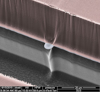
A scanning electron micrograph shows a nano-SPEAR suspended midway between layers of silicon (grey) and photoresist material (pink) that form a recording chamber for immobilized nematodes. The high-throughput technology developed at Rice University can be adapted for other small animals and could enhance data-gathering for disease characterization and drug interactions. Courtesy of the Robinson Lab

Here’s a link to and a citation for the paper,

Scalable electrophysiology in intact small animals with nanoscale suspended electrode arrays by Daniel L. Gonzales, Krishna N. Badhiwala, Daniel G. Vercosa, Benjamin W. Avants, Zheng Liu, Weiwei Zhong, & Jacob T. Robinson. Nature Nanotechnology (2017) doi:10.1038/nnano.2017.55 Published online 17 April 2017

This paper is behind a paywall.

Weaving at the nanoscale

A Jan. 21, 2016 news item on ScienceDaily announces a brand new technique,

For the first time, scientists have been able to weave a material at molecular level. The research is led by University of California Berkeley, in cooperation with Stockholm University. …

A Jan. 21, 2016 Stockholm University press release, which originated the news item, provides more information,

Weaving is a well-known way of making fabric, but has until now never been used at the molecular level. Scientists have now been able to weave organic threads into a three-dimensional material, using copper as a template. The new material is a COF, covalent organic framework, and is named COF-505. The copper ions can be removed and added without changing the underlying structure, and at the same time the elasticity can be reversibly changed.

– It almost looks like a molecular version of the Vikings chain-armour. The material is very flexible, says Peter Oleynikov, researcher at the Department of Materials and Environmental Chemistry at Stockholm University.

COF’s are like MOF’s porous three-dimensional crystals with a very large internal surface that can adsorb and store enormous quantities of molecules. A potential application is capture and storage of carbon dioxide, or using COF’s as a catalyst to make useful molecules from carbon dioxide.

Complex structure determined in Stockholm

The research is led by Professor Omar Yaghi at University of California Berkeley. At Stockholm University Professor Osamu Terasaki, PhD Student Yanhang Ma and Researcher Peter Oleynikov have contributed to determine the structure of COF-505 at atomic level from a nano-crystal, using electron crystallography methods.

– It is a difficult, complicated structure and it was very demanding to resolve. We’ve spent lot of time and efforts on the structure solution. Now we know exactly where the copper is and we can also replace the metal. This opens up many possibilities to make other materials, says Yanhang Ma, PhD Student at the Department of Materials and Environmental Chemistry at Stockholm University.

Another of the collaborating institutions, US Department of Energy Lawrence Berkeley National Laboratory issued a Jan. 21, 2016 news release on EurekAlert, providing a different perspective and some additional details,

There are many different ways to make nanomaterials but weaving, the oldest and most enduring method of making fabrics, has not been one of them – until now. An international collaboration led by scientists at the U.S. Department of Energy (DOE)’s Lawrence Berkeley National Laboratory (Berkeley Lab) and the University of California (UC) Berkeley, has woven the first three-dimensional covalent organic frameworks (COFs) from helical organic threads. The woven COFs display significant advantages in structural flexibility, resiliency and reversibility over previous COFs – materials that are highly prized for their potential to capture and store carbon dioxide then convert it into valuable chemical products.

“Weaving in chemistry has been long sought after and is unknown in biology,” Yaghi says [Omar Yaghi, chemist who holds joint appointments with Berkeley Lab’s Materials Sciences Division and UC Berkeley’s Chemistry Department and is the co-director of the Kavli Energy NanoScience Institute {Kavli-ENSI}]. “However, we have found a way of weaving organic threads that enables us to design and make complex two- and three-dimensional organic extended structures.”

COFs and their cousin materials, metal organic frameworks (MOFs), are porous three-dimensional crystals with extraordinarily large internal surface areas that can absorb and store enormous quantities of targeted molecules. Invented by Yaghi, COFs and MOFs consist of molecules (organics for COFs and metal-organics for MOFs) that are stitched into large and extended netlike frameworks whose structures are held together by strong chemical bonds. Such frameworks show great promise for, among other applications, carbon sequestration.

Through another technique developed by Yaghi, called “reticular chemistry,” these frameworks can also be embedded with catalysts to carry out desired functions: for example, reducing carbon dioxide into carbon monoxide, which serves as a primary building block for a wide range of chemical products including fuels, pharmaceuticals and plastics.

In this latest study, Yaghi and his collaborators used a copper(I) complex as a template for bringing threads of the organic compound “phenanthroline” into a woven pattern to produce an immine-based framework they dubbed COF-505. Through X-ray and electron diffraction characterizations, the researchers discovered that the copper(I) ions can be reversibly removed or restored to COF-505 without changing its woven structure. Demetalation of the COF resulted in a tenfold increase in its elasticity and remetalation restored the COF to its original stiffness.

“That our system can switch between two states of elasticity reversibly by a simple operation, the first such demonstration in an extended chemical structure, means that cycling between these states can be done repeatedly without degrading or altering the structure,” Yaghi says. “Based on these results, it is easy to imagine the creation of molecular cloths that combine unusual resiliency, strength, flexibility and chemical variability in one material.”

Yaghi says that MOFs can also be woven as can all structures based on netlike frameworks. In addition, these woven structures can also be made as nanoparticles or polymers, which means they can be fabricated into thin films and electronic devices.

“Our weaving technique allows long threads of covalently linked molecules to cross at regular intervals,” Yaghi says. “These crossings serve as points of registry, so that the threads have many degrees of freedom to move away from and back to such points without collapsing the overall structure, a boon to making materials with exceptional mechanical properties and dynamics.”

###

This research was primarily supported by BASF (Germany) and King Abdulaziz City for Science and Technology (KACST).

It’s unusual that neither Stockholm University not the Lawrence Berkeley National Laboratory list all of the institutions involved. To get a sense of this international collaboration’s size, I’m going to list them,

  • 1Department of Chemistry, University of California, Berkeley, Materials Sciences Division, Lawrence Berkeley National Laboratory, and Kavli Energy NanoSciences Institute, Berkeley, CA 94720, USA.
  • 2Department of Materials and Environmental Chemistry, Stockholm University, SE-10691 Stockholm, Sweden.
  • 3Department of New Architectures in Materials Chemistry, Materials Science Institute of Madrid, Consejo Superior de Investigaciones Científicas, Madrid 28049, Spain.
  • 4Nanomaterials Research Institute, National Institute of Advanced Industrial Science and Technology (AIST), Tsukuba 305-8565, Japan.
  • 5NSF Nanoscale Science and Engineering Center (NSEC), University of California at Berkeley, 3112 Etcheverry Hall, Berkeley, CA 94720, USA.
  • 6Advanced Light Source, Lawrence Berkeley National Laboratory, Berkeley, CA 94720, USA.
  • 7King Abdulaziz City of Science and Technology, Post Office Box 6086, Riyadh 11442, Saudi Arabia.
  • 8Material Sciences Division, Lawrence Berkeley National Laboratory, 1 Cyclotron Road, Berkeley, CA 94720, USA.
  • 9School of Physical Science and Technology, ShanghaiTech University, Shanghai 201210, China.

Given that some of the money came from a German company, I’m surprised not one German institution was involved.

Here’s a link to and citation for the paper,

Weaving of organic threads into a crystalline covalent organic framework by Yuzhong Liu, Yanhang Ma, Yingbo Zhao, Xixi Sun, Felipe Gándara, Hiroyasu Furukawa, Zheng Liu, Hanyu Zhu, Chenhui Zhu, Kazutomo Suenaga, Peter Oleynikov, Ahmad S. Alshammari, Xiang Zhang, Osamu Terasaki, Omar M. Yaghi. Science  22 Jan 2016: Vol. 351, Issue 6271, pp. 365-369 DOI: 10.1126/science.aad4011

This paper is behind a paywall.

Cute, adorable roundworms help measure nanoparticle toxicity

Caption: Low-cost experiments to test the toxicity of nanomaterials focused on populations of roundworms. Rice University scientists were able to test 20 nanomaterials in a short time, and see their method as a way to determine which nanomaterials should undergo more extensive testing. Credit: Zhong Lab/Rice University

Caption: Low-cost experiments to test the toxicity of nanomaterials focused on populations of roundworms. Rice University scientists were able to test 20 nanomaterials in a short time, and see their method as a way to determine which nanomaterials should undergo more extensive testing.
Credit: Zhong Lab/Rice University

Until now, ‘cute’ and ‘adorable’ are not words I would have associated with worms of any kind or with Rice University, for that matter. It’s amazing what a single image can do, eh?

A Feb. 3, 2015 news item on Azonano describes how roundworms have been used in research investigating the toxicity of various kinds of nanoparticles,

The lowly roundworm is the star of an ambitious Rice University project to measure the toxicity of nanoparticles.

The low-cost, high-throughput study by Rice scientists Weiwei Zhong and Qilin Li measures the effects of many types of nanoparticles not only on individual organisms but also on entire populations.

A Feb. 2, 2015 Rice University news release (also on EurekAlert), which originated the news item, provides more details about the research,

The Rice researchers tested 20 types of nanoparticles and determined that five, including the carbon-60 molecules (“buckyballs”) discovered at Rice in 1985, showed little to no toxicity.

Others were moderately or highly toxic to Caenorhabditis elegans, several generations of which the researchers observed to see the particles’ effects on their health.

The results were published by the American Chemical Society journal Environmental Sciences and Technology. They are also available on the researchers’ open-source website.

“Nanoparticles are basically new materials, and we don’t know much about what they will do to human health and the health of the ecosystem,” said Li, an associate professor of civil and environmental engineering and of materials science and nanoengineering. “There have been a lot of publications showing certain nanomaterials are more toxic than others. So before we make more products that incorporate these nanomaterials, it’s important that we understand we’re not putting anything toxic into the environment or into consumer products.

“The question is, How much cost can we bear?” she said. “It’s a long and expensive process to do a thorough toxicological study of any chemical, not just nanomaterials.” She said that due to the large variety of nanomaterials being produced at high speed and at such a large scale, there is “an urgent need for high-throughput screening techniques to prioritize which to study more extensively.”

Rice’s pilot study proves it is possible to gather a lot of toxicity data at low cost, said Zhong, an assistant professor of biosciences, who has performed extensive studies on C. elegans, particularly on their gene networks. Materials alone for each assay, including the worms and the bacteria they consumed and the culture media, cost about 50 cents, she said.

The researchers used four assays to see how worms react to nanoparticles: fitness, movement, growth and lifespan. The most sensitive assay of toxicity was fitness. In this test, the researchers mixed the nanoparticles in solutions with the bacteria that worms consume. Measuring how much bacteria they ate over time served as a measure of the worms’ “fitness.”

“If the worms’ health is affected by the nanoparticles, they reproduce less and eat less,” Zhong said. “In the fitness assay, we monitor the worms for a week. That is long enough for us to monitor toxicity effects accumulated through three generations of worms.” C. elegans has a life cycle of about three days, and since each can produce many offspring, a population that started at 50 would number more than 10,000 after a week. Such a large number of tested animals also enabled the fitness assay to be highly sensitive.

The researchers’ “QuantWorm” system allowed fast monitoring of worm fitness, movement, growth and lifespan. In fact, monitoring the worms was probably the least time-intensive part of the project. Each nanomaterial required specific preparation to make sure it was soluble and could be delivered to the worms along with the bacteria. The chemical properties of each nanomaterial also needed to be characterized in detail.

The researchers studied a representative sampling of three classes of nanoparticles: metal, metal oxides and carbon-based. “We did not do polymeric nanoparticles because the type of polymers you can possibly have is endless,” Li explained.

They examined the toxicity of each nanoparticle at four concentrations. Their results showed C-60 fullerenes, fullerol (a fullerene derivative), titanium dioxide, titanium dioxide-decorated nanotubes and cerium dioxide were the least damaging to worm populations.

Their “fitness” assay confirmed dose-dependent toxicity for carbon black, single- and multiwalled carbon nanotubes, graphene, graphene oxide, gold nanoparticles and fumed silicon dioxide.

They also determined the degree to which surface chemistry affected the toxicity of some particles. While amine-functionalized multiwalled nanotubes proved highly toxic, hydroxylated nanotubes had the least toxicity, with significant differences in fitness, body length and lifespan.

A complete and interactive toxicity chart for all of the tested materials is available online.

Zhong said the method could prove its worth as a rapid way for drug or other companies to narrow the range of nanoparticles they wish to put through more expensive, dedicated toxicology testing.

“Next, we hope to add environmental variables to the assays, for example, to mimic ultraviolet exposure or river water conditions in the solution to see how they affect toxicity,” she said. “We also want to study the biological mechanism by which some particles are toxic to worms.”

Here’s a citation for the paper and links to the paper and to the researchers’ website,

A multi-endpoint, high-throughput study of nanomaterial toxicity in Caenorhabditis elegans by Sang-Kyu Jung, Xiaolei Qu, Boanerges Aleman-Meza, Tianxiao Wang, Celeste Riepe, Zheng Liu, Qilin Li, and Weiwei Zhong. Environ. Sci. Technol., Just Accepted Manuscript DOI: 10.1021/es5056462 Publication Date (Web): January 22, 2015
Copyright © 2015 American Chemical Society

Nanomaterial effects on C. elegans

Home | Download | Tutorial | About

This heat map indicates whether a measurement for the nanomaterial-exposed worms is higher (yellow), or lower (blue) than the control worms. Black indicates no effects from nanomaterial exposure.

Clicking on colored blocks to see detailed experimental data.

The published paper is open access but you need an American Chemical Society site registration to access it. The researchers’ site is open access.

Nestling a two-element atomic chain inside a carbon nanotube

While there doesn’t seem to be a short-term application for this research from Japan, the idea of nestling a chain of two elements inside a carbon nanotube is intriguing, from an Oct. 16, 2014 news item on Nanowerk,

Kazutomo Suenaga of the Nanotube Research Center (NTRC) of the National Institute of Advanced Industrial Science and Technology (AIST) and Ryosuke Senga of the Nano-carbon Characterization Team, NTRC, AIST, have synthesized an atomic chain in which two elements are aligned alternately and have evaluated its physical properties on an atomic level.

An ionic crystalline atomic chain of cesium iodine (CsI) has been synthesized by aligning a cesium ion (Cs+), a cation and an iodine ion (I-), an anion, alternately by encapsulating CsI in the microscopic space inside a carbon nanotube. Furthermore, by using an advanced aberration-corrected electron microscope, the physical phenomena unique to the CsI atomic chain, such as the difference in dynamic behavior of its cations and anions, have been discovered. In addition, from theoretical calculation using density functional theory (DFT), this CsI atomic chain has been found to indicate different optical properties from a three-dimensional CsI crystal, and applications to new optical devices are anticipated.

An Oct. 16, 2014 National Institute of Advanced Industrial Science and Technology (AIST) press release, which originated the news item, situates the research within a social and historical context,

Social Background of Research

In the accelerating and ballooning information society, electronic devices used in computers and smartphones has constantly demanded higher performance and efficiency. The materials currently drawing expectations are low-dimensional materials with a single to few-atom width and thickness. Two-dimensional materials, typified by graphene, indicate unique physical characteristics not found in three-dimensional materials, such as its excellent electrical transport properties, and are being extensively researched.

An atomic chain, which has an even finer structure with a width of only one atom, has been predicted to display excellent electrical transport properties, like two-dimensional materials. Although expectations were higher than for two-dimensional materials from the viewpoint of integration, it had attracted little attention until now. This is because of the technological difficulties faced by the various processes of academic research from synthesis to analysis of atomic chains, and academic understanding has not progressed far (Fig. 1).

Figure 1
Figure 1 : Transition of target materials in material research

History of Research

AIST has been developing element analysis methods on a single-atom level to detect certain special structures including impurities, dopants and defects, that affect the properties of low-dimensional materials such as carbon nanotubes and graphene (AIST press releases on July 6, 2009, January 12, 2010, December 16, 2010 and July 9, 2012). In this research, efforts were made for the synthesis and analysis of the atomic chain, a low-dimensional material, using the accumulated technological expertise. This research has been supported by both the Strategic Basic Research Program of the Japan Science and Technology Agency (FY2012 to FY2016), and the Grants-in-aid for Scientific Research of the Japan Society for the Promotion of Science, “Development of elemental technology for the atomic-scale evaluation and application of low-dimensional materials using nano-space” (FY2014 to FY2016).

The press release also offers more details about the research and future applications,

Details of Research

The developed technology is the technology to expose carbon nanotubes, with a diameter of 1 nm or smaller, to CsI vapor to encapsulate CsI in the microscopic space inside the carbon nanotubes, to synthesize an atomic chain in which two elements, Cs and I, are aligned alternately. Furthermore, by combining aberration-corrected electron microscopy and an electronic spectroscopic technique known as electron energy-loss spectroscopy (EELS) detailed structural analysis of this atomic chain was conducted. In order to identify each atom aligned at a distance of 1 nm or less without destroying them, the accelerating voltage of the electron microscope was significantly lowered to 60 kV to reduce damage to the sample by electron beams, while maintaining sufficient spatial resolution of around 1 nm. Figure 2 indicates the smallest CsI crystal confirmed so far, and the CsI atomic chain synthesized in this research.

Figure 2
Figure 2 : Comparison of CsI atomic chain and CsI crystal
(Top: Actual annular dark-field images, Bottom: Corresponding models)

Figure 3 shows the annular dark-field (ADF) image of the CsI atomic chain and the element mapping for Cs and I, respectively, obtained by EELS. It can be seen that the two elements are aligned alternately. There has not been any report of this simple and ideal structure actually being produced and observed, and it can be said to be a fundamental, important finding in material science.

Normally, in an ADF image, those with larger atomic numbers appear brighter. However, in this CsI atomic chain, I (atomic number 53) appears brighter than Cs (atomic number 55). This is because Cs, being a cation, moves more actively (more accurately, the total amount of electrons scattered by the Cs atom is not very different from those of the I atom, but the electrons scattered by the moving Cs atom generate spatial expansion), indicating a difference in dynamic behavior of the cation and the anion that cannot occur in a large three-dimensional crystal. Locations where single Cs atom or I atom is absent, namely vacancies, were also found (Fig. 3, right).

The unique behavior and structure influence various physical properties. When optical absorption spectra were calculated using DFT, the response of the CsI atomic chain to light differed with the direction of incidence. Furthermore, it was found that in a CsI atomic chain with vacancies, the electron state of vacancy sites where the I atom is absent possess a donor level at which electrons were easily released, while vacancy sites where the Cs atom is absent possess a receptor level at which electrons were easily received. By making use of these physical properties, applications to new electro-optical devices, such as a micro-light source and an optical switch using light emission from a single vacancy in the CsI atomic chain, are conceivable. In addition, further research into combinations of other elements triggered by the present results may lead to the development of new materials and device applications. There are expectations for atomic chains to be the next-generation materials for devices in search of further miniaturization and integration.

Figure 3
Figure 3 : Synthesized CsI atomic chain, encapsulated in double-walled carbon nanotube
(From left: ADF image, element maps for Cs and I, model, ADF image of CsI atomic chains with vacancies)

Future Plans

Since the CsI atomic chain displays optical properties significantly different from large crystals that can be seen by the human eye, there are expectations for its application for new electro-optical devices such as a micro-light source and an optical switch using light emission from a single vacancy in the CsI atomic chain. The researchers will conduct experimental research in its application, focused on detailed study of its various physical properties, starting with its optical properties. In addition to CsI, efforts will also be made in the development of new materials that combine various elements, by applying this technology to other materials.

Furthermore, the mechanism of all adsorbents of radioactive substances (carbon nanotubes, zeolite, Prussian blue, etc.) currently being developed for commercial use are methods of encapsulating radioactive atoms inside microscopic space in the material. The researchers hope to utilize the knowledge of the behavior of the Cs atom in a microscopic space obtained in this research, to improve adsorption performance.

Here’s a link to and a citation for the research paper,

Atomic structure and dynamic behaviour of truly one-dimensional ionic chains inside ​carbon nanotubes by Ryosuke Senga, Hannu-Pekka Komsa, Zheng Liu, Kaori Hirose-Takai, Arkady V. Krasheninnikov, & Kazu Suenaga. Nature Materials (2014) doi:10.1038/nmat4069 Published online 14 September 2014

This paper is behind a paywall.

Serendipity and coaxial nanocables

I like the sound of the word coaxial especially when it’s used in conjunction with cable, as in coaxial cable. Adding the world serendipity to the mix, as they did at Rice University, made the June 7, 2012 news item by Jade Boyd on the Nanowerk website irresistible [Note: I have removed a link.],

Thanks to a little serendipity, researchers at Rice University have created a tiny coaxial cable that is about a thousand times smaller than a human hair and has higher capacitance than previously reported microcapacitors.

The nanocable, which is described this week in Nature Communications (“Anomalous high capacitance in a coaxial single nanowire capacitor” [behind paywall]), was produced with techniques pioneered in the nascent graphene research field and could be used to build next-generation energy-storage systems. It could also find use in wiring up components of lab-on-a-chip processors, but its discovery is owed partly to chance.

“We didn’t expect to create this when we started,” said study co-author Jun Lou, associate professor of mechanical engineering and materials science at Rice. “At the outset, we were just curious to see what would happen electrically and mechanically if we took small copper wires known as interconnects and covered them with a thin layer of carbon.”

Boyd’s June 7, 2012 news item can also be read in its entirety at the Rice University website [Note: I have removed some links.],

The tiny coaxial cable is remarkably similar in makeup to the ones that carry cable television signals into millions of homes and offices. The heart of the cable is a solid copper wire that is surrounded by a thin sheath of insulating copper oxide. A third layer, another conductor, surrounds that. In the case of TV cables, the third layer is copper again, but in the nanocable it is a thin layer of carbon measuring just a few atoms thick. The coax nanocable is about 100 nanometers, or 100 billionths of a meter, wide.

While the coaxial cable is a mainstay of broadband telecommunications, the three-layer, metal-insulator-metal structure can also be used to build energy-storage devices called capacitors. Unlike batteries, which rely on chemical reactions to both store and supply electricity, capacitors use electrical fields. A capacitor contains two electrical conductors, one negative and the other positive, that are separated by thin layer of insulation. Separating the oppositely charged conductors creates an electrical potential, and that potential increases as the separated charges increase and as the distance between them – occupied by the insulating layer — decreases. The proportion between the charge density and the separating distance is known as capacitance, and it’s the standard measure of efficiency of a capacitor.

The study reports that the capacitance of the nanocable is at least 10 times greater than what would be predicted with classical electrostatics.

“The increase is most likely due to quantum effects that arise because of the small size of the cable,” said study co-author Pulickel Ajayan, Rice’s Benjamin M. and Mary Greenwood Anderson Professor of Mechanical Engineering and Materials Science.

When the project began 18 months ago, Rice postdoctoral researcher Zheng Liu, the lead co-author of the study, intended to make pure copper wires covered with carbon. The techniques for making the wires, which are just a few nanometers wide, are well-established because the wires are often used as “interconnects” in state-of-the-art electronics. Liu used a technique known as chemical vapor deposition (CVD) to cover the wires with a thin coating of carbon. The CVD technique is also used to grow sheets of single-atom-thick carbon called graphene on films of copper.

“When people make graphene, they usually want to study the graphene and they aren’t very interested in the copper,” Lou said. “It’s just used a platform for making the graphene.”

When Liu ran some electronic tests on his first few samples, the results were far from what he expected.

“We eventually found that a thin layer of copper oxide — which is served as a dielectric layer — was forming between the copper and the carbon,” said Liu.

Here’s an image illustrating this process,

The three-layer coaxial nanocable contains a solid copper wire surrounded by a layer of copper oxide that is encased a layer of carbon just a few atoms thick. (Courtesy: Rice University)

The researchers don’t seem to have any particular applications in mind for their nancoaxial cable although they seem hopeful about a few possibilities (from the June 7, 2012 news item on the Rice University website,

The capacitance of the new nanocable is up to 143 microfarads per centimeter squared, better than the best previous results from microcapacitors.

Lou said it may be possible to build a large-scale energy-storage device by arranging millions of the tiny nanocables side by side in large arrays.

“The nanoscale cable might also be used as a transmission line for radio frequency signals at the nanoscale,” Liu said. “This could be useful as a fundamental building block in micro- and nano-sized electromechanical systems like lab-on-a-chip devices.”

Who knows where serendipity will take this discovery?

As for why that word made the item irresistible to me, many years ago I was at a dinner party and one of the guests (a vivid storyteller and born in Sri Lanka) explained the origin of the word, serendipity. Sadly I don’t remember the details of her story, so here’s a less rich version of the story from the Encyclopedia Britannia website,

Serendib, also spelled Serendip, Arabic Sarandīb, name for the island of Sri Lanka (Ceylon). The name, Arabic in origin, was recorded in use at least as early as ad 361 and for a time gained considerable currency in the West. It is best known to speakers of English through the word serendipity, invented in the 18th century by the English man of letters Horace Walpole on the inspiration of a Persian fairy tale, “The Three Princes of Serendip,” whose heroes often made discoveries by chance.