Category Archives: electronics

ChatGPT and a neuromorphic (brainlike) synapse

I was teaching an introductory course about nanotechnology back in 2014 and, at the end of a session, stated (more or less) that the full potential for artificial intelligence (software) wasn’t going to be perceived until the hardware (memistors) was part of the package. (It’s interesting to revisit that in light of the recent uproar around AI (covered in my May 25, 2023 posting, which offered a survey of the situation.)

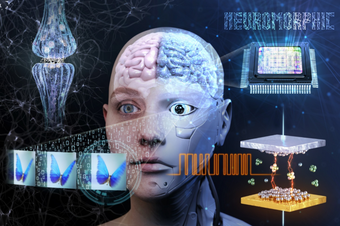
One of the major problems with artificial intelligence is its memory. The other is energy consumption. Both problems could be addressed by the integration of memristors into the hardware, giving rise to neuromorphic (brainlike) computing. (For those who don’t know, the human brain in addition to its capacity for memory is remarkably energy efficient.)

This is the first time I’ve seen research into memristors where software has been included. Disclaimer: There may be a lot more research of this type; I just haven’t seen it before. A March 24, 2023 news item on ScienceDaily announces research from Korea,

ChatGPT’s impact extends beyond the education sector and is causing significant changes in other areas. The AI language model is recognized for its ability to perform various tasks, including paper writing, translation, coding, and more, all through question-and-answer-based interactions. The AI system relies on deep learning, which requires extensive training to minimize errors, resulting in frequent data transfers between memory and processors. However, traditional digital computer systems’ von Neumann architecture separates the storage and computation of information, resulting in increased power consumption and significant delays in AI computations. Researchers have developed semiconductor technologies suitable for AI applications to address this challenge.

A March 24, 2023 Pohang University of Science & Technology (POSTECH) press release (also on EurekAlert), which originated the news item, provides more detail,

A research team at POSTECH, led by Professor Yoonyoung Chung (Department of Electrical Engineering, Department of Semiconductor Engineering), Professor Seyoung Kim (Department of Materials Science and Engineering, Department of Semiconductor Engineering), and Ph.D. candidate Seongmin Park (Department of Electrical Engineering), has developed a high-performance AI semiconductor device [emphasis mine] using indium gallium zinc oxide (IGZO), an oxide semiconductor widely used in OLED [organic light-emitting diode] displays. The new device has proven to be excellent in terms of performance and power efficiency.

Efficient AI operations, such as those of ChatGPT, require computations to occur within the memory responsible for storing information. Unfortunately, previous AI semiconductor technologies were limited in meeting all the requirements, such as linear and symmetric programming and uniformity, to improve AI accuracy.

The research team sought IGZO as a key material for AI computations that could be mass-produced and provide uniformity, durability, and computing accuracy. This compound comprises four atoms in a fixed ratio of indium, gallium, zinc, and oxygen and has excellent electron mobility and leakage current properties, which have made it a backplane of the OLED display.

Using this material, the researchers developed a novel synapse device [emphasis mine] composed of two transistors interconnected through a storage node. The precise control of this node’s charging and discharging speed has enabled the AI semiconductor to meet the diverse performance metrics required for high-level performance. Furthermore, applying synaptic devices to a large-scale AI system requires the output current of synaptic devices to be minimized. The researchers confirmed the possibility of utilizing the ultra-thin film insulators inside the transistors to control the current, making them suitable for large-scale AI.

The researchers used the newly developed synaptic device to train and classify handwritten data, achieving a high accuracy of over 98%, [emphasis mine] which verifies its potential application in high-accuracy AI systems in the future.

Professor Chung explained, “The significance of my research team’s achievement is that we overcame the limitations of conventional AI semiconductor technologies that focused solely on material development. To do this, we utilized materials already in mass production. Furthermore, Linear and symmetrical programming characteristics were obtained through a new structure using two transistors as one synaptic device. Thus, our successful development and application of this new AI semiconductor technology show great potential to improve the efficiency and accuracy of AI.”

This study was published last week [March 2023] on the inside back cover of Advanced Electronic Materials [paper edition] and was supported by the Next-Generation Intelligent Semiconductor Technology Development Program through the National Research Foundation, funded by the Ministry of Science and ICT [Information and Communication Technologies] of Korea.

Here’s a link to and a citation for the paper,

Highly Linear and Symmetric Analog Neuromorphic Synapse Based on Metal Oxide Semiconductor Transistors with Self-Assembled Monolayer for High-Precision Neural Network Computatio by Seongmin Park, Suwon Seong, Gilsu Jeon, Wonjae Ji, Kyungmi Noh, Seyoung Kim, Yoonyoung Chun. Volume 9, Issue 3 March 2023 2200554 DOI: https://doi.org/10.1002/aelm.202200554 First published online: 29 December 2022

This paper is open access.

Also, there is another approach to using materials such as indium gallium zinc oxide (IGZO) for a memristor. That would be using biological cells as my June 6, 2023 posting, which features work on biological neural networks (BNNs), suggests in relation to creating robots that can perform brainlike computing.

Future firefighters and wearable technology

I imagine this wearable technology would also be useful for the military too. However, the focus for these researchers from China is firefighting. (Given the situation with the Canadian wildfires in June 2023, we have 10x more than the average at this time in the season over the last 10 years, it’s good to see some work focused on safety for firefighters.) From a January 17, 2023 news item on phys.org,

Firefighting may look vastly different in the future thanks to intelligent fire suits and masks developed by multiple research institutions in China.

Researchers published results showing breathable electrodes woven into fabric used in fire suits have proven to be stable at temperatures over 520ºC. At these temperatures, the fabric is found to be essentially non-combustible with high rates of thermal protection time.

Caption: Scientists from multiple institutions address the challenges and limitations of current fire-fighting gear by introducing wearable, breathable sensors and electrodes to better serve firefighters. Credit: Nano Research, Tsinghua University Press

A January 17, 2023 Tsinghua University Press press release on EurekAlert, which originated the news item, provides more technical details,

The results show the efficacy and practicality of Janus graphene/poly(p-phenylene benzobisoxazole), or PBO, woven fabric in making firefighting “smarter” with the main goal being to manufacture products on an industrial scale that are flame-retardant but also intelligent enough to warn the firefighter of increased risks while traversing the flames.

“Conventional firefighting clothing and fire masks can ensure firemen’s safety to a certain extent,” said Wei Fan, professor at the School of Textile Science and Engineering at Xi’an Polytechnic University. “However, the fire scene often changes quickly, sometimes making firefighters trapped in the fire for failing to judge the risks in time. At this situation, firefighters also need to be rescued.”

The key here is the use of Janus graphene/PBO, woven fabrics. While not the first of its kind, the introduction of PBO fibers offers better strength and fire protection than other similar fibers, such as Kevlar. The PBO fibers are first woven into a fabric that is then irradiated using a CO2 infrared laser. From here, the fabric becomes the Janus graphene/PBO hybrid that is the focus of the study.   

The mask also utilizes a top and bottom layer of Janus graphene/PBO with a piezoelectric layer in between that acts as a way to convert mechanical pressures to electricity.

“The mask has a good smoke particle filtration effect, and the filtration efficiency of PM2.5 and PM3.0 reaches 95% and 100%, respectively. Meanwhile, the mask has good wearing comfort as its respiratory resistance (46.8 Pa) is lower than 49 Pa of commercial masks. Besides, the mask is sensitive to the speed and intensity of human breathing, which can dynamically monitor the health of the firemen” said Fan.

Flame-retardant electronics featured in these fire suits are flexible, heat resistant, quick to make and low-cost which makes scaling for industrial production a tangible achievement. This makes it more likely that the future of firefighting suits and masks will be able to effectively use this technology. Quick, effective responses can also reduce economic losses attributed to fires.

“The graphene/PBO woven fabrics-based sensors exhibit good repeatability and stability in human motion monitoring and NO2 gas detection, the main toxic gas in fires, which can be applied to firefighting suits to help firefighters effectively avoiding danger” Fan said. Being able to detect sharp increases in NO2 gas can help firefighters change course in an instant if needed and could be a lifesaving addition to firefighter gear.

Major improvements can be made in the firefighting field to better protect the firefighters by taking advantage of graphene/PBO woven and nonwoven fabrics. Widescale use of this technology can help the researchers reach their ultimate goal of reducing mortality and injury to those who risk their lives fighting fires.

Yu Luo and Yaping Miao of the School of Textile Science and Engineering at Xi’an Polytechnic University contributed equally to this work. Professor Wei Fan is the corresponding author. Yingying Zhang and Huimin Wang of the Department of Chemistry at Tsinghua University, Kai Dong of the Beijing Institute of Nanoenergy and Nanosystems at the Chinese Academy of Sciences, and Lin Hou and Yanyan Xu of Shaanxi Textile Research Institute Co., LTD, Weichun Chen and Yao Zhang of the School of Textile Science and Engineering at Xi’an Polytechnic University contributed to this research. 

This work was supported by the National Natural Science Foundation of China, Textile Vision Basic Research Program of China, Key Research and Development Program of Xianyang Science and Technology Bureau, Key Research and Development Program of Shaanxi Province, Natural Science Foundation of Shaanxi Province, and Scientific Research Project of Shaanxi Provincial Education Department.

Here are two links and a citation for the same paper,

Laser-induced Janus graphene/poly(p-phenylene benzobisoxazole) fabrics with intrinsic flame retardancy as flexible sensors and breathable electrodes for fire-fighting field by Yu Luo, Yaping Miao, Huimin Wang, Kai Dong, Lin Hou, Yanyan Xu, Weichun Chen, Yao Zhang, Yingying Zhang & Wei Fan. Nano Research (2023) DOI: https://doi.org/10.1007/s12274-023-5382-y Published12 January 2023

This link leads to a paywall.

Here’s the second link (to SciOpen)

Laser-induced Janus graphene/poly(p-phenylene benzobisoxazole) fabrics with intrinsic flame retardancy as flexible sensors and breathable electrodes for fire-fighting field. SciOpen Published January 12, 2023

This link leads to an open access journal published by Tsinghua University Press.

Artificial organic neuron mimics characteristics of biological nerve cells

There’s a possibility that in the future, artificial neurons could be used for medical treatment according to a January 12, 2023 news item on phys.org,

Researchers at Linköping University (LiU), Sweden, have created an artificial organic neuron that closely mimics the characteristics of biological nerve cells. This artificial neuron can stimulate natural nerves, making it a promising technology for various medical treatments in the future.

Work to develop increasingly functional artificial nerve cells continues at the Laboratory for Organic Electronics, LOE. In 2022, a team of scientists led by associate professor Simone Fabiano demonstrated how an artificial organic neuron could be integrated into a living carnivorous plant [emphasis mine] to control the opening and closing of its maw. This synthetic nerve cell met two of the 20 characteristics that differentiate it from a biological nerve cell.

I wasn’t expecting a carnivorous plant, living or otherwise. Sadly, they don’t seem to have been able to include it in this image although the ‘green mitts’ are evocative,

Caption: Artificial neurons created by the researchers at Linköping University. Credit: Thor Balkhed

A January 13, 2023 Linköping University (LiU) press release by Mikael Sönne (also on EurkeAlert but published January 12, 2023), which originated the news item, delves further into the work,

In their latest study, published in the journal Nature Materials, the same researchers at LiU have developed a new artificial nerve cell called “conductance-based organic electrochemical neuron” or c-OECN, which closely mimics 15 out of the 20 neural features that characterise biological nerve cells, making its functioning much more similar to natural nerve cells.

“One of the key challenges in creating artificial neurons that effectively mimic real biological neurons is the ability to incorporate ion modulation. Traditional artificial neurons made of silicon can emulate many neural features but cannot communicate through ions. In contrast, c-OECNs use ions to demonstrate several key features of real biological neurons”, says Simone Fabiano, principal investigator of the Organic Nanoelectronics group at LOE.

In 2018, this research group at Linköping University was one of the first to develop organic electrochemical transistors based on n-type conducting polymers, which are materials that can conduct negative charges. This made it possible to build printable complementary organic electrochemical circuits. Since then, the group has been working to optimise these transistors so that they can be printed in a printing press on a thin plastic foil. As a result, it is now possible to print thousands of transistors on a flexible substrate and use them to develop artificial nerve cells.

In the newly developed artificial neuron, ions are used to control the flow of electronic current through an n-type conducting polymer, leading to spikes in the device’s voltage. This process is similar to that which occurs in biological nerve cells. The unique material in the artificial nerve cell also allows the current to be increased and decreased in an almost perfect bell-shaped curve that resembles the activation and inactivation of sodium ion channels found in biology.

“Several other polymers show this behaviour, but only rigid polymers are resilient to disorder, enabling stable device operation”, says Simone Fabiano

In experiments carried out in collaboration with Karolinska Institute (KI), the new c-OECN neurons were connected to the vagus nerve of mice. The results show that the artificial neuron could stimulate the mice’s nerves, causing a 4.5% change in their heart rate.

The fact that the artificial neuron can stimulate the vagus nerve itself could, in the long run, pave the way for essential applications in various forms of medical treatment. In general, organic semiconductors have the advantage of being biocompatible, soft, and malleable, while the vagus nerve plays a key role, for example, in the body’s immune system and metabolism.

The next step for the researchers will be to reduce the energy consumption of the artificial neurons, which is still much higher than that of human nerve cells. Much work remains to be done to replicate nature artificially.

“There is much we still don’t fully understand about the human brain and nerve cells. In fact, we don’t know how the nerve cell makes use of many of these 15 demonstrated features. Mimicking the nerve cells can enable us to understand the brain better and build circuits capable of performing intelligent tasks. We’ve got a long road ahead, but this study is a good start,” says Padinhare Cholakkal Harikesh, postdoc and main author of the scientific paper.

Here’s a link to and a citation for the paper,

Ion-tunable antiambipolarity in mixed ion–electron conducting polymers enables biorealistic organic electrochemical neurons by Padinhare Cholakkal Harikesh, Chi-Yuan Yang, Han-Yan Wu, Silan Zhang, Mary J. Donahue, April S. Caravaca, Jun-Da Huang, Peder S. Olofsson, Magnus Berggren, Deyu Tu & Simone Fabiano. Nature Materials volume 22, pages 242–248 (2023) DOI: https://doi.org/10.1038/s41563-022-01450-8 Published online: 12 January 2023 Issue Date: February 2023

This paper is open access.

Graphene-based nanoelectronics platform, a replacement for silicon?

A December 31, 2022 news item on phys.org describes research into replacing silicon in the field of electronics, Note: Links have been removed,

A pressing quest in the field of nanoelectronics is the search for a material that could replace silicon. Graphene has seemed promising for decades. But its potential has faltered along the way, due to damaging processing methods and the lack of a new electronics paradigm to embrace it. With silicon nearly maxed out in its ability to accommodate faster computing, the next big nanoelectronics platform is needed now more than ever.

Walter de Heer, Regents’ Professor in the School of Physics at the Georgia Institute of Technology [Georgia Tech], has taken a critical step forward in making the case for a successor to silicon. De Heer and his collaborators have developed a new nanoelectronics platform based on graphene—a single sheet of carbon atoms. The technology is compatible with conventional microelectronics manufacturing, a necessity for any viable alternative to silicon.

In the course of their research, published in Nature Communications, the team may have also discovered a new quasiparticle. Their discovery could lead to manufacturing smaller, faster, more efficient and more sustainable computer chips, and has potential implications for quantum and high-performance computing.

A January 3, 2023 Georgia Institute of Technology news release (also on EurekAlert but published December 21, 2022] by Catherine Barzler, which originated the news item, delves further into the work

“Graphene’s power lies in its flat, two-dimensional structure that is held together by the strongest chemical bonds known,” de Heer said. “It was clear from the beginning that graphene can be miniaturized to a far greater extent than silicon — enabling much smaller devices, while operating at higher speeds and producing much less heat. This means that, in principle, more devices can be packed on a single chip of graphene than with silicon.”

In 2001, de Heer proposed an alternative form of electronics based on epitaxial graphene, or epigraphene — a layer of graphene that was found to spontaneously form on top of silicon carbide crystal, a semiconductor used in high power electronics. At the time, researchers found that electric currents flow without resistance along epigraphene’s edges, and that graphene devices could be seamlessly interconnected without metal wires. This combination allows for a form of electronics that relies on the unique light-like properties of graphene electrons.

“Quantum interference has been observed in carbon nanotubes at low temperatures, and we expect to see similar effects in epigraphene ribbons and networks,” de Heer said. “This important feature of graphene is not possible with silicon.”

Building the Platform

To create the new nanoelectronics platform, the researchers created a modified form of epigraphene on a silicon carbide crystal substrate. In collaboration with researchers at the Tianjin International Center for Nanoparticles and Nanosystems at the University of Tianjin, China, they produced unique silicon carbide chips from electronics-grade silicon carbide crystals. The graphene itself was grown at de Heer’s laboratory at Georgia Tech using patented furnaces.

The researchers used electron beam lithography, a method commonly used in microelectronics, to carve the graphene nanostructures and weld their edges to the silicon carbide chips. This process mechanically stabilizes and seals the graphene’s edges, which would otherwise react with oxygen and other gases that might interfere with the motion of the charges along the edge.

Finally, to measure the electronic properties of their graphene platform, the team used a cryogenic apparatus that allows them to record its properties from a near-zero temperature to room temperature.

Observing the Edge State

The electric charges the team observed in the graphene edge state were similar to photons in an optical fiber that can travel over large distances without scattering. They found that the charges traveled for tens of thousands of nanometers along the edge before scattering. Graphene electrons in previous technologies could only travel about 10 nanometers before bumping into small imperfections and scattering in different directions.

“What’s special about the electric charges in the edges is that they stay on the edge and keep on going at the same speed, even if the edges are not perfectly straight,” said Claire Berger, physics professor at Georgia Tech and director of research at the French National Center for Scientific Research in Grenoble, France.

In metals, electric currents are carried by negatively charged electrons. But contrary to the researchers’ expectations, their measurements suggested that the edge currents were not carried by electrons or by holes (a term for positive quasiparticles indicating the absence of an electron). Rather, the currents were carried by a highly unusual quasiparticle that has no charge and no energy, and yet moves without resistance. The components of the hybrid quasiparticle were observed to travel on opposite sides of the graphene’s edges, despite being a single object.

The unique properties indicate that the quasiparticle might be one that physicists have been hoping to exploit for decades — the elusive Majorana fermion predicted by Italian theoretical physicist Ettore Majorana in 1937.

“Developing electronics using this new quasiparticle in seamlessly interconnected graphene networks is game changing,” de Heer said.

It will likely be another five to 10 years before we have the first graphene-based electronics, according to de Heer. But thanks to the team’s new epitaxial graphene platform, technology is closer than ever to crowning graphene as a successor to silicon.

Here’s a link to and a citation for the paper,

An epitaxial graphene platform for zero-energy edge state nanoelectronics by Vladimir S. Prudkovskiy, Yiran Hu, Kaimin Zhang, Yue Hu, Peixuan Ji, Grant Nunn, Jian Zhao, Chenqian Shi, Antonio Tejeda, David Wander, Alessandro De Cecco, Clemens B. Winkelmann, Yuxuan Jiang, Tianhao Zhao, Katsunori Wakabayashi, Zhigang Jiang, Lei Ma, Claire Berger & Walt A. de Heer. Nature Communications volume 13, Article number: 7814 (2022) DOI: https://doi.org/10.1038/s41467-022-34369-4 Published 19 December 2022

This paper is open access.

Analogue memristor for next-generation brain-mimicking (neuromorphic) computing

This research into an analogue memristor comes from The Korea Institute of Science and Technology (KIST) according to a September 20, 2022 news item on Nanowerk, Note: A link has been removed,

Neuromorphic computing system technology mimicking the human brain has emerged and overcome the limitation of excessive power consumption regarding the existing von Neumann computing method. A high-performance, analog artificial synapse device, capable of expressing various synapse connection strengths, is required to implement a semiconductor device that uses a brain information transmission method. This method uses signals transmitted between neurons when a neuron generates a spike signal.

However, considering conventional resistance-variable memory devices widely used as artificial synapses, as the filament grows with varying resistance, the electric field increases, causing a feedback phenomenon, resulting in rapid filament growth. Therefore, it is challenging to implement considerable plasticity while maintaining analog (gradual) resistance variation concerning the filament type.

The Korea Institute of Science and Technology (KIST), led by Dr. YeonJoo Jeong’s team at the Center for Neuromorphic Engineering, solved the limitations of analog synaptic characteristics, plasticity and information preservation, which are chronic obstacles regarding memristors, neuromorphic semiconductor devices. He announced the development of an artificial synaptic semiconductor device capable of highly reliable neuromorphic computing (Nature Communications, “Cluster-type analogue memristor by engineering redox dynamics for high-performance neuromorphic computing”).

Caption: Concept image of the article Credit: Korea Institute of Science and Technology (KIST)

A September 20, 2022 (Korea) National Research Council of Science & Technology press release on EurekAlert, which originated the news item, delves further into the research,

The KIST research team fine-tuned the redox properties of active electrode ions to solve small synaptic plasticity hindering the performance of existing neuromorphic semiconductor devices. Furthermore, various transition metals were doped and used in the synaptic device, controlling the reduction probability of active electrode ions. It was discovered that the high reduction probability of ions is a critical variable in the development of high-performance artificial synaptic devices.

Therefore, a titanium transition metal, having a high ion reduction probability, was introduced by the research team into an existing artificial synaptic device. This maintains the synapse’s analog characteristics and the device plasticity at the synapse of the biological brain, approximately five times the difference between high and low resistances. Furthermore, they developed a high-performance neuromorphic semiconductor that is approximately 50 times more efficient.

Additionally, due to the high alloy formation reaction concerning the doped titanium transition metal, the information retention increased up to 63 times compared with the existing artificial synaptic device. Furthermore, brain functions, including long-term potentiation and long-term depression, could be more precisely simulated.

The team implemented an artificial neural network learning pattern using the developed artificial synaptic device and attempted artificial intelligence image recognition learning. As a result, the error rate was reduced by more than 60% compared with the existing artificial synaptic device; additionally, the handwriting image pattern (MNIST) recognition accuracy increased by more than 69%. The research team confirmed the feasibility of a high-performance neuromorphic computing system through this improved the artificial synaptic device.

Dr. Jeong of KIST stated, “This study drastically improved the synaptic range of motion and information preservation, which were the greatest technical barriers of existing synaptic mimics.” “In the developed artificial synapse device, the device’s analog operation area to express the synapse’s various connection strengths has been maximized, so the performance of brain simulation-based artificial intelligence computing will be improved.” Additionally, he mentioned, “In the follow-up research, we will manufacture a neuromorphic semiconductor chip based on the developed artificial synapse device to realize a high-performance artificial intelligence system, thereby further enhancing competitiveness in the domestic system and artificial intelligence semiconductor field.”

Here’s a link to and a citation for the paper,

Cluster-type analogue memristor by engineering redox dynamics for high-performance neuromorphic computing by Jaehyun Kang, Taeyoon Kim, Suman Hu, Jaewook Kim, Joon Young Kwak, Jongkil Park, Jong Keuk Park, Inho Kim, Suyoun Lee, Sangbum Kim & YeonJoo Jeong. Nature Communications volume 13, Article number: 4040 (2022) DOI: https://doi.org/10.1038/s41467-022-31804-4 Published: 12 July 2022

This paper is open access.

Dynamic molecular switches for brainlike computing at the University of Limerick

Aren’t memristors proof that brainlike computing at the molecular and atomic levels is possible? It seems I have misunderstood memristors according to this November 21, 2022 news item on ScienceDaily,

A breakthrough discovery at University of Limerick in Ireland has revealed for the first time that unconventional brain-like computing at the tiniest scale of atoms and molecules is possible.

Researchers at University of Limerick’s Bernal Institute worked with an international team of scientists to create a new type of organic material that learns from its past behaviour.

The discovery of the ‘dynamic molecular switch’ that emulate[s] synaptic behaviour is revealed in a new study in the international journal Nature Materials.

The study was led by Damien Thompson, Professor of Molecular Modelling in UL’s Department of Physics and Director of SSPC, the UL-hosted Science Foundation Ireland Research Centre for Pharmaceuticals, together with Christian Nijhuis at the Centre for Molecules and Brain-Inspired Nano Systems in University of Twente [Netherlands] and Enrique del Barco from University of Central Florida.

A November 21, 2022 University of Limerick press release (also on EurekAlert), which originated the news item, provides more technical details about the research,

Working during lockdowns, the team developed a two-nanometre thick layer of molecules, which is 50,000 times thinner than a strand of hair and remembers its history as electrons pass through it.

Professor Thompson explained that the “switching probability and the values of the on/off states continually change in the molecular material, which provides a disruptive new alternative to conventional silicon-based digital switches that can only ever be either on or off”.

The newly discovered dynamic organic switch displays all the mathematical logic functions necessary for deep learning, successfully emulating Pavlovian ‘call and response’ synaptic brain-like behaviour.

The researchers demonstrated the new materials properties using extensive experimental characterisation and electrical measurements supported by multi-scale modelling spanning from predictive modelling of the molecular structures at the quantum level to analytical mathematical modelling of the electrical data.

To emulate the dynamical behaviour of synapses at the molecular level, the researchers combined fast electron transfer (akin to action potentials and fast depolarization processes in biology) with slow proton coupling limited by diffusion (akin to the role of biological calcium ions or neurotransmitters).

Since the electron transfer and proton coupling steps inside the material occur at very different time scales, the transformation can emulate the plastic behaviour of synapse neuronal junctions, Pavlovian learning, and all logic gates for digital circuits, simply by changing the applied voltage and the duration of voltage pulses during the synthesis, they explained.

“This was a great lockdown project, with Chris, Enrique and I pushing each other through zoom meetings and gargantuan email threads to bring our teams combined skills in materials modelling, synthesis and characterisation to the point where we could demonstrate these new brain-like computing properties,” explained Professor Thompson.

“The community has long known that silicon technology works completely differently to how our brains work and so we used new types of electronic materials based on soft molecules to emulate brain-like computing networks.”

The researchers explained that the method can in the future be applied to dynamic molecular systems driven by other stimuli such as light and coupled to different types of dynamic covalent bond formation.

This breakthrough opens up a whole new range of adaptive and reconfigurable systems, creating new opportunities in sustainable and green chemistry, from more efficient flow chemistry production of drug products and other value-added chemicals to development of new organic materials for high density computing and memory storage in big data centres.

“This is just the start. We are already busy expanding this next generation of intelligent molecular materials, which is enabling development of sustainable alternative technologies to tackle grand challenges in energy, environment, and health,” explained Professor Thompson.

Professor Norelee Kennedy, Vice President Research at UL, said: “Our researchers are continuously finding new ways of making more effective, more sustainable materials. This latest finding is very exciting, demonstrating the reach and ambition of our international collaborations and showcasing our world-leading ability at UL to encode useful properties into organic materials.”

Here’s a link to and a citation for the paper,

Dynamic molecular switches with hysteretic negative differential conductance emulating synaptic behaviour by Yulong Wang, Qian Zhang, Hippolyte P. A. G. Astier, Cameron Nickle, Saurabh Soni, Fuad A. Alami, Alessandro Borrini, Ziyu Zhang, Christian Honnigfort, Björn Braunschweig, Andrea Leoncini, Dong-Cheng Qi, Yingmei Han, Enrique del Barco, Damien Thompson & Christian A. Nijhuis. Nature Materials volume 21, pages 1403–1411 (2022) DOI: https://doi.org/10.1038/s41563-022-01402-2 Published: 21 November 2022 Issue Date: December 2022

This paper is behind a paywall.

Transforming bacterial cells into living computers

If this were a movie instead of a press release, we’d have some ominous music playing over a scene in a pristine white lab. Instead, we have a November 13, 2022 Technion-Israel Institute of Technology press release (also on EurekAlert) where the writer tries to highlight the achievement while downplaying the sort of research (in synthetic biology) that could have people running for the exits,

Bringing together concepts from electrical engineering and bioengineering tools, Technion and MIT [Massachusetts Institute of Technology] scientists collaborated to produce cells engineered to compute sophisticated functions – “biocomputers” of sorts. Graduate students and researchers from Technion – Israel Institute of Technology Professor Ramez Daniel’s Laboratory for Synthetic Biology & Bioelectronics worked together with Professor Ron Weiss from the Massachusetts Institute of Technology to create genetic “devices” designed to perform computations like artificial neural circuits. Their results were recently published in Nature Communications.

The genetic material was inserted into the bacterial cell in the form of a plasmid: a relatively short DNA molecule that remains separate from the bacteria’s “natural” genome. Plasmids also exist in nature, and serve various functions. The research group designed the plasmid’s genetic sequence to function as a simple computer, or more specifically, a simple artificial neural network. This was done by means of several genes on the plasmid regulating each other’s activation and deactivation according to outside stimuli.

What does it mean that a cell is a circuit? How can a computer be biological?

At its most basic level, a computer consists of 0s and 1s, of switches. Operations are performed on these switches: summing them, picking the maximal or minimal value between them, etc. More advanced operations rely on the basic ones, allowing a computer to play chess or fly a rocket to the moon.

In the electronic computers we know, the 0/1 switches take the form of transistors. But our cells are also computers, of a different sort. There, the presence or absence of a molecule can act as a switch. Genes activate, trigger or suppress other genes, forming, modifying, or removing molecules. Synthetic biology aims (among other goals) to harness these processes, to synthesize the switches and program the genes that would make a bacterial cell perform complex tasks. Cells are naturally equipped to sense chemicals and to produce organic molecules. Being able to “computerize” these processes within the cell could have major implications for biomanufacturing and have multiple medical applications.

The Ph.D students (now doctors) Luna Rizik and Loai Danial, together with Dr. Mouna Habib, under the guidance of Prof. Ramez Daniel from the Faculty of Biomedical Engineering at the Technion, and in collaboration with Prof. Ron Weiss from the Synthetic Biology Center, MIT,  were inspired by how artificial neural networks function. They created synthetic computation circuits by combining existing genetic “parts,” or engineered genes, in novel ways, and implemented concepts from neuromorphic electronics into bacterial cells. The result was the creation of bacterial cells that can be trained using artificial intelligence algorithms.

The group were able to create flexible bacterial cells that can be dynamically reprogrammed to switch between reporting whether at least one of a test chemicals, or two, are present (that is, the cells were able to switch between performing the OR and the AND functions). Cells that can change their programming dynamically are capable of performing different operations under different conditions. (Indeed, our cells do this naturally.) Being able to create and control this process paves the way for more complex programming, making the engineered cells suitable for more advanced tasks. Artificial Intelligence algorithms allowed the scientists to produce the required genetic modifications to the bacterial cells at a significantly reduced time and cost.

Going further, the group made use of another natural property of living cells: they are capable of responding to gradients. Using artificial intelligence algorithms, the group succeeded in harnessing this natural ability to make an analog-to-digital converter – a cell capable of reporting whether the concentration of a particular molecule is “low”, “medium”, or “high.” Such a sensor could be used to deliver the correct dosage of medicaments, including cancer immunotherapy and diabetes drugs.

Of the researchers working on this study, Dr. Luna Rizik and Dr. Mouna Habib hail from the Department of Biomedical Engineering, while Dr. Loai Danial is from the Andrew and Erna Viterbi Faculty of Electrical Engineering. It is bringing the two fields together that allowed the group to make the progress they did in the field of synthetic biology.

This work was partially funded by the Neubauer Family Foundation, the Israel Science Foundation (ISF), European Union’s Horizon 2020 Research and Innovation Programme, the Technion’s Lorry I. Lokey interdisciplinary Center for Life Sciences and Engineering, and the [US Department of Defense] Defense Advanced Research Projects Agency [DARPA].

Here’s a link to and a citation for the paper,

Synthetic neuromorphic computing in living cells by Luna Rizik, Loai Danial, Mouna Habib, Ron Weiss & Ramez Daniel. Nature Communications volume 13, Article number: 5602 (2022) DOIL https://doi.org/10.1038/s41467-022-33288-8 Published: 24 September 2022

This paper is open access.

Graphene can be used in quantum components

A November 3, 2022 news item on phys.org provides a brief history of graphene before announcing the latest work from ETH Zurich,

Less than 20 years ago, Konstantin Novoselov and Andre Geim first created two-dimensional crystals consisting of just one layer of carbon atoms. Known as graphene, this material has had quite a career since then.

Due to its exceptional strength, graphene is used today to reinforce products such as tennis rackets, car tires or aircraft wings. But it is also an interesting subject for fundamental research, as physicists keep discovering new, astonishing phenomena that have not been observed in other materials.

The right twist

Bilayer graphene crystals, in which the two atomic layers are slightly rotated relative to each other, are particularly interesting for researchers. About one year ago, a team of researchers led by Klaus Ensslin and Thomas Ihn at ETH Zurich’s Laboratory for Solid State Physics was able to demonstrate that twisted graphene could be used to create Josephson junctions, the fundamental building blocks of superconducting devices.

Based on this work, researchers were now able to produce the first superconducting quantum interference device, or SQUID, from twisted graphene for the purpose of demonstrating the interference of superconducting quasiparticles. Conventional SQUIDs are already being used, for instance in medicine, geology and archaeology. Their sensitive sensors are capable of measuring even the smallest changes in magnetic fields. However, SQUIDs work only in conjunction with superconducting materials, so they require cooling with liquid helium or nitrogen when in operation.

In quantum technology, SQUIDs can host quantum bits (qubits); that is, as elements for carrying out quantum operations. “SQUIDs are to superconductivity what transistors are to semiconductor technology—the fundamental building blocks for more complex circuits,” Ensslin explains.

A November 3, 2022 ETH Zurich news release by Felix Würsten, which originated the news item, delves further into the work,

The spectrum is widening

The graphene SQUIDs created by doctoral student Elías Portolés are not more sensitive than their conventional counterparts made from aluminium and also have to be cooled down to temperatures lower than 2 degrees above absolute zero. “So it’s not a breakthrough for SQUID technology as such,” Ensslin says. However, it does broaden graphene’s application spectrum significantly. “Five years ago, we were already able to show that graphene could be used to build single-electron transistors. Now we’ve added superconductivity,” Ensslin says.

What is remarkable is that the graphene’s behaviour can be controlled in a targeted manner by biasing an electrode. Depending on the voltage applied, the material can be insulating, conducting or superconducting. “The rich spectrum of opportunities offered by solid-state physics is at our disposal,” Ensslin says.

Also interesting is that the two fundamental building blocks of a semiconductor (transistor) and a superconductor (SQUID) can now be combined in a single material. This makes it possible to build novel control operations. “Normally, the transistor is made from silicon and the SQUID from aluminium,” Ensslin says. “These are different materials requiring different processing technologies.”

An extremely challenging production process

Superconductivity in graphene was discovered by an MIT [Massachusetts Institute of Technology] research group five years ago, yet there are only a dozen or so experimental groups worldwide that look at this phenomenon. Even fewer are capable of converting superconducting graphene into a functioning component.

The challenge is that scientists have to carry out several delicate work steps one after the other: First, they have to align the graphene sheets at the exact right angle relative to each other. The next steps then include connecting electrodes and etching holes. If the graphene were to be heated up, as happens often during cleanroom processing, the two layers re-align the twist angle vanishes. “The entire standard semiconductor technology has to be readjusted, making this an extremely challenging job,” Portolés says.

The vision of hybrid systems

Ensslin is thinking one step ahead. Quite a variety of different qubit technologies are currently being assessed, each with its own advantages and disadvantages. For the most part, this is being done by various research groups within the National Center of Competence in Quantum Science and Technology (QSIT). If scientists succeed in coupling two of these systems using graphene, it might be possible to combine their benefits as well. “The result would be two different quantum systems on the same crystal,” Ensslin says.

This would also generate new possibilities for research on superconductivity. “With these components, we might be better able to understand how superconductivity in graphene comes about in the first place,” he adds. “All we know today is that there are different phases of superconductivity in this material, but we do not yet have a theoretical model to explain them.”

Here’s a link to and a citation for the paper,

A tunable monolithic SQUID in twisted bilayer graphene by Elías Portolés, Shuichi Iwakiri, Giulia Zheng, Peter Rickhaus, Takashi Taniguchi, Kenji Watanabe, Thomas Ihn, Klaus Ensslin & Folkert K. de Vries. Nature Nanotechnology volume 17, pages 1159–1164 (2022) Issue Date: November 2022 DOI: https://doi.org/10.1038/s41565-022-01222-0 Published online: 24 October 2022

This paper is behind a paywall.

Plant fibers (nanocellulose) for more sustainable devices

Thank you to Junichiro Shiomi and the University of Tokyo for this image,

Caption: An artist’s interpretation of the way natural cellulose fibers are combined to form the CNF [cellulose nanofiber] yarn, and a magnified section showing the nanoscopic rod-shaped filaments within the yarn bundle. Credit: ©2022 Junichiro Shiomi

The research into cellulose nanofibers (CNFs) announced in this November 4, 2022 news item on ScienceDaily comes from the University of Tokyo,

Plant-derived materials such as cellulose often exhibit thermally insulating properties. A new material made from nanoscale cellulose fibers shows the reverse, high thermal conductivity. This makes it useful in areas previously dominated by synthetic polymer materials. Materials based on cellulose have environmental benefits over polymers, so research on this could lead to greener technological applications where thermal conductivity is needed.

Both cellulose nanofibers/nanofibres and cellulose nanofibrils are abbreviated to CNFs. This seems a bit confusing so I went looking for an explanation and found this September 22, 2020 posting (scroll down about 35% of the way) by professor Hatsuo Ishida, Department of Macromolecular Science and Engineering at Case Western Reserve University,

Both fiber and fibril indicate long thread-like materials and their meanings are essentially the same. However, the word,”fibril,” emphasizes a thin fiber. Therefore, the use of the word, “nano fibril,” is rather redundant. The word,”fibril” is often used for distinguishing high temperature water vapor treated cellulose fibers that are spread into very thin fibers from the whiskers prepared by the acid treatment of cellulosic materials. The word,” microfibril” is more often used than “nano fibril.” Some also use the word,”cellulose nanocrystal.” Cellulose whiskers are single crystals of materials and a typical length is less than a micrometer (one of the longest cellulose whiskers can be prepared from a sea creature called tunicate), whereas the cellulose nano fibril has much longer length. This material is much easier to scale up whereas cellulose whiskers are not as easily scale up as the nano fibrils. The word fiber has no implication and it is simply a thread like object. Thus, even if the diameter is more than hundred micrometers, as long as the length is much longer (high aspect ratio), you may call it a fiber, whereas such a thick fiber is seldom called a fibril.

Thank you professor Ishida!

A November 4, 2022 University of Tokyo press release (also on EurekAlert), which originated the news item, explains the interest in nanocellulose and its thermal properties,

Cellulose is a key structural component of plant cell walls and is the reason why trees can grow to such heights. But the secret of its material strength actually lies in its overlapping nanoscopic fibers. In recent years, many commercial products have used cellulose nanofiber (CNF) materials because their strength and durability make them a good replacement for polymer-based materials such as plastics that can be detrimental to the environment. But now and for the first time, a research team led by Professor Junichiro Shiomi from the University of Tokyo’s Graduate School of Engineering has investigated previously unknown thermal properties of CNF, and their findings show these materials could be even more useful still.

“If you see plant-derived materials such as cellulose or woody biomass used in applications, it’s typically mechanical or thermally insulating properties that are being employed,” said Shiomi. “When we explored the thermal properties of a yarn made from CNF, however, we found that they show a different kind of thermal behavior, thermal conduction, and it’s very significant, around 100 times higher than that of typical woody biomass or cellulose paper.”

The reason yarn made from CNF can conduct heat so well is due to the way it’s made. Cellulose fibers in nature are very disorganized, but a process called the flow-focusing method combines cellulose fibers, orientating them in the same way, to create CNF. It’s this tightly bound and aligned bundle of rod-shaped fibers that allows heat to transfer along the bundle, whereas in a more chaotic structure it would dissipate heat more readily.

“Our main challenge was how to measure the thermal conductivity of such small physical samples and with great accuracy,” said Shiomi. “For this, we turned to a technique called T-type thermal conductivity measurement. It allowed us to measure the thermal conductivity of the rod-shaped CNF yarn samples which are only micrometers (a micrometer equaling one-thousandth of a millimeter) in diameter. But the next step for us is to perform accurate thermal tests on two-dimensional textilelike samples.”

Shiomi and his team hope that their investigation and future explorations into the use of CNF as a thermally conductive material could give engineers an alternative to some environmentally damaging polymers. In applications where heat transfer is important, such as certain electronic or computational components, it could greatly reduce the consequences of discarded electronic equipment, or e-waste, thanks to the biodegradable nature of CNF and other plant-based materials.

Here’s a link to and a citation for the paper,

Enhanced High Thermal Conductivity Cellulose Filaments via Hydrodynamic Focusing by Guantong Wang, Masaki Kudo, Kazuho Daicho, Sivasankaran Harish, Bin Xu, Cheng Shao, Yaerim Lee, Yuxuan Liao, Naoto Matsushima, Takashi Kodama, Fredrik Lundell, L. Daniel Söderberg, Tsuguyuki Saito, and Junichiro Shiomi. Nano Lett. 2022, 22, 21, 8406–8412 DOI: https://doi.org/10.1021/acs.nanolett.2c02057 Publication Date:October 25, 2022 Copyright © 2022 The Authors. Published by American Chemical Society

This paper is open access.

Bioinspired ‘smart’ materials a step towards soft robotics and electronics

An October 13, 2022 news item on Nanowerk describes some new work from the University of Texas at Austin,

Inspired by living things from trees to shellfish, researchers at The University of Texas at Austin set out to create a plastic much like many life forms that are hard and rigid in some places and soft and stretchy in others.

Their success — a first, using only light and a catalyst to change properties such as hardness and elasticity in molecules of the same type — has brought about a new material that is 10 times as tough as natural rubber and could lead to more flexible electronics and robotics.

An October 13, 2022 University of Texas at Austin news release (also on EurekAlert), which originated the news item, delves further into the work,

“This is the first material of its type,” said Zachariah Page, assistant professor of chemistry and corresponding author on the paper. “The ability to control crystallization, and therefore the physical properties of the material, with the application of light is potentially transformative for wearable electronics or actuators in soft robotics.”

Scientists have long sought to mimic the properties of living structures, like skin and muscle, with synthetic materials. In living organisms, structures often combine attributes such as strength and flexibility with ease. When using a mix of different synthetic materials to mimic these attributes, materials often fail, coming apart and ripping at the junctures between different materials.

Oftentimes, when bringing materials together, particularly if they have very different mechanical properties, they want to come apart,” Page said. Page and his team were able to control and change the structure of a plastic-like material, using light to alter how firm or stretchy the material would be.

Chemists started with a monomer, a small molecule that binds with others like it to form the building blocks for larger structures called polymers that were similar to the polymer found in the most commonly used plastic. After testing a dozen catalysts, they found one that, when added to their monomer and shown visible light, resulted in a semicrystalline polymer similar to those found in existing synthetic rubber. A harder and more rigid material was formed in the areas the light touched, while the unlit areas retained their soft, stretchy properties.

Because the substance is made of one material with different properties, it was stronger and could be stretched farther than most mixed materials.

The reaction takes place at room temperature, the monomer and catalyst are commercially available, and researchers used inexpensive blue LEDs as the light source in the experiment. The reaction also takes less than an hour and minimizes use of any hazardous waste, which makes the process rapid, inexpensive, energy efficient and environmentally benign.

The researchers will next seek to develop more objects with the material to continue to test its usability.

“We are looking forward to exploring methods of applying this chemistry towards making 3D objects containing both hard and soft components,” said first author Adrian Rylski, a doctoral student at UT Austin.

The team envisions the material could be used as a flexible foundation to anchor electronic components in medical devices or wearable tech. In robotics, strong and flexible materials are desirable to improve movement and durability.

Here’s a link to and a citation for the paper,

Polymeric multimaterials by photochemical patterning of crystallinity by Adrian K. Rylski, Henry L. Cater, Keldy S. Mason, Marshall J. Allen, Anthony J. Arrowood, Benny D. Freeman, Gabriel E. Sanoja, and Zachariah A. Page. Science 13 Oct 2022 Vol 378, Issue 6616 pp. 211-215 DOI: 10.1126/science.add6975

This paper is behind a paywall.