Monthly Archives: June 2019

Non-viral ocular gene therapy with gold nanoparticles and femtosecond lasers

I love the stylistic choice the writer made (pay special attention to the second paragraph) when producing this November 19, 2018 Polytechnique Montréal news release (also on EurekAlert),

A scientific breakthrough by Professor Michel Meunier of Polytechnique Montréal and his collaborators offers hope for people with glaucoma, retinitis or macular degeneration.

In January 2009, the life of engineer Michel Meunier, a professor at Polytechnique Montréal, changed dramatically. Like others, he had observed that the extremely short pulse of a femtosecond laser (0.000000000000001 second) could make nanometre-sized holes appear in silicon when it was covered by gold nanoparticles. But this researcher, recognized internationally for his skills in laser and nanotechnology, decided to go a step further with what was then just a laboratory curiosity. He wondered if it was possible to go from silicon to living matter, from inorganic to organic. Could the gold nanoparticles and the femtosecond laser, this “light scalpel,” reproduce the same phenomenon with living cells?

A very pretty image illustrating the work,

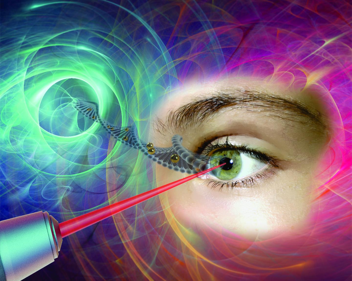
Caption: Gold nanoparticles, which act like “nanolenses,” concentrate the energy produced by the extremely short pulse of a femtosecond laser to create a nanoscale incision on the surface of the eye’s retina cells. This technology, which preserves cell integrity, can be used to effectively inject drugs or genes into specific areas of the eye, offering new hope to people with glaucoma, retinitis or macular degeneration. Credit and Copyright: Polytechnique Montréal

The news release goes on to describe the technology in more detail,

Professor Meunier started working on cells in vitro in his Polytechnique laboratory. The challenge was to make a nanometric incision in the cells’ extracellular membrane without damaging it. Using gold nanoparticles that acted as “nanolenses,” Professor Meunier realized that it was possible to concentrate the light energy coming from the laser at a wavelength of 800 nanometres. Since there is very little energy absorption by the cells at this wavelength, their integrity is preserved. Mission accomplished!

Based on this finding, Professor Meunier decided to work on cells in vivo, cells that are part of a complex living cell structure, such as the eye for example.

The eye and the light scalpel

In April 2012, Professor Meunier met Przemyslaw Sapieha, an internationally renowned eye specialist, particularly recognized for his work on the retina. “Mike”, as he goes by, is a professor in the Department of Ophthalmology at Université de Montréal and a researcher at Centre intégré universitaire de santé et de services sociaux (CIUSSS) de l’Est-de-l’Île-de-Montréal. He immediately saw the potential of this new technology and everything that could be done in the eye if you could block the ripple effect that occurs following a trigger that leads to glaucoma or macular degeneration, for example, by injecting drugs, proteins or even genes.

Using a femtosecond laser to treat the eye–a highly specialized and fragile organ–is very complex, however. The eye is part of the central nervous system, and therefore many of the cells or families of cells that compose it are neurons. And when a neuron dies, it does not regenerate like other cells do. Mike Sapieha’s first task was therefore to ensure that a femtosecond laser could be used on one or several neurons without affecting them. This is what is referred to as “proof of concept.”

Proof of concept

Mike and Michel called on biochemistry researcher Ariel Wilson, an expert in eye structures and vision mechanisms, as well as Professor Santiago Costantino and his team from the Department of Ophthalmology at Université de Montréal and the CIUSSS de l’Est-de-l’Île-de-Montréal for their expertise in biophotonics. The team first decided to work on healthy cells, because they are better understood than sick cells. They injected gold nanoparticles combined with antibodies to target specific neuronal cells in the eye, and then waited for the nanoparticles to settle around the various neurons or families of neurons, such as the retina. Following the bright flash generated by the femtosecond laser, the expected phenomenon occurred: small holes appeared in the cells of the eye’s retina, making it possible to effectively inject drugs or genes in specific areas of the eye. It was another victory for Michel Meunier and his collaborators, with these conclusive results now opening the path to new treatments.

The key feature of the technology developed by the researchers from Polytechnique and CIUSSS de l’Est-de-l’Île-de-Montréal is its extreme precision. With the use of functionalized gold nanoparticles, the light scalpel makes it possible to precisely locate the family of cells where the doctor will have to intervene.

Having successfully demonstrated proof of concept, Professor Meunier and his team filed a patent application in the United States. This tremendous work was also the subject of a paper reviewed by an impressive reading committee and published in the renowned journal Nano Letters in October 2018.

While there is still a lot of research to be done–at least 10 years’ worth, first on animals and then on humans–this technology could make all the difference in an aging population suffering from eye deterioration for which there are still no effective long-term treatments. It also has the advantage of avoiding the use of viruses commonly employed in gene therapy. These researchers are looking at applications of this technology in all eye diseases, but more particularly in glaucoma, retinitis and macular degeneration.

This light scalpel is unprecedented.

Here’s a link to and a citation for the paper,

In Vivo Laser-Mediated Retinal Ganglion Cell Optoporation Using KV1.1 Conjugated Gold Nanoparticles by Ariel M. Wilson, Javier Mazzaferri, Éric Bergeron, Sergiy Patskovsky, Paule Marcoux-Valiquette, Santiago Costantino, Przemyslaw Sapieha, Michel Meunier. Nano Lett.201818116981-6988 DOI: https://doi.org/10.1021/acs.nanolett.8b02896 Publication Date: October 4, 2018  Copyright © 2018 American Chemical Society

This paper is behind a paywall.

Brief note about changes

June 19,2019: Hello! I apologize for this site’s unavailability over the last 10 days or so (June 7 – 18, 2019). Moving to a new web hosting service meant that the ‘law of unintended consequences’ came into play. Fingers crossed that all the problems have been resolved.

On another matter, I’ve accumulated quite a backlog of postings, which I will be resizing (publishing) over the next few months. I’ve been trying to bring that backlog down to a reasonable size for quite some time now but I see more drastic, focused action is required. I will continue posting some more recent news items along with my older pieces.

Two-dimensional arsenic (arsenene) for electronics

Another day, another ‘ene’ (e.g., graphene, borene, germanene, etc.). This ‘ene’ is arsenene, from an October 15, 2018 Wiley (Publications) news release (also on EurekAlert),

The discovery of graphene, a material made of one or very few atomic layers of carbon, started a boom. Today, such two-dimensional materials are no longer limited to carbon and are hot prospects for many applications, especially in microelectronics. In the journal Angewandte Chemie, scientists have now introduced a new 2D material: they successfully modified arsenene (arsenic in a graphene-like structure) with chloromethylene groups.

Two-dimensional materials are crystalline materials made of just a single or very few layers of atoms that often display unusual properties. However, the use of graphene for applications such as transistors is limited because it behaves more like a conductor than a semiconductor. Modified graphene and 2D materials based on other chemical elements with semiconducting properties have now been developed. One such material is β-arsenene, a two-dimensional arsenic in a buckled honeycomb structure derived from gray arsenic. Researchers hope that modification of this previously seldom-studied material could improve its semiconducting properties and lead the way to new applications in fields such as sensing, catalysis, optoelectronics, and other semiconductor technologies.

A team at the University of Chemistry and Technology Prague (Czech Republic) and Nanyang Technical University (Singapore), led by Zdenek Sofer and Martin Pumera has now successfully produced a highly promising covalent modification of β-arsenene.

The arsenene was produced by milling gray arsenic in tetrahydrofuran. The shear forces cause two-dimensional layers to split off and disperse into the solvent. The researchers then introduce dichloromethane and add an organic lithium compound (butyllithium). These two reagents form an intermediate called chlorocarbene, a molecule made of one carbon atom, one hydrogen atom, and one chlorine atom. The carbon atom is short two bonding partners, a state that makes the whole class of carbene molecules highly reactive. Arsenene contains free electron pairs that “stick out” from the surface and can easily enter into bonds to chlorocarbene.

This approach leads to high coverage of the arsenene surface with chloromethylene groups, as confirmed by a variety of analysis methods (X-ray photoelectron spectroscopy, FT-IR spectroscopy, elemental analysis by transmission electron microscopy). The modified arsenene is more stable than pure arsenene and exhibits strong luminescence and electronic properties that make it attractive for optoelectronic applications. In addition, the chloromethylene units could serve as a starting point for further interesting modifications.

As always with an ‘ene’, the major focus is on electronics. Here’s a link to and a citation for the paper,

Covalent Functionalization of Exfoliated Arsenic with Chlorocarbene by Jiri Sturala, Adriano Ambrosi, Zdeněk Sofer, Martin Pumera. Angewandte Chimie International Edition Volume 57, Issue 45 November 5, 2018 Pages 14837-14840 DOI: https://doi.org/10.1002/anie.201809341 First published: 31 August 2018

This paper is behind a paywall.

Making nanoscale transistor chips out of thin air—sort of

Caption: The nano-gap transistors operating in air. As gaps become smaller than the mean-free path of electrons in air, there is ballistic electron transport. Credit: RMIT University

A November 19, 2018 news item on Nanowerk describes the ‘airy’ work ( Note: A link has been removed),

Researchers at RMIT University [Ausralia] have engineered a new type of transistor, the building block for all electronics. Instead of sending electrical currents through silicon, these transistors send electrons through narrow air gaps, where they can travel unimpeded as if in space.

The device unveiled in material sciences journal Nano Letters (“Metal–Air Transistors: Semiconductor-free field-emission air-channel nanoelectronics”), eliminates the use of any semiconductor at all, making it faster and less prone to heating up.

A November 19, 2018 RMIT University news release on EurkeAlert, which originated the news item, describes the work and possibilities in more detail,

Lead author and PhD candidate in RMIT’s Functional Materials and Microsystems Research Group, Ms Shruti Nirantar, said this promising proof-of-concept design for nanochips as a combination of metal and air gaps could revolutionise electronics.

“Every computer and phone has millions to billions of electronic transistors made from silicon, but this technology is reaching its physical limits where the silicon atoms get in the way of the current flow, limiting speed and causing heat,” Nirantar said.

“Our air channel transistor technology has the current flowing through air, so there are no collisions to slow it down and no resistance in the material to produce heat.”

The power of computer chips – or number of transistors squeezed onto a silicon chip – has increased on a predictable path for decades, roughly doubling every two years. But this rate of progress, known as Moore’s Law, has slowed in recent years as engineers struggle to make transistor parts, which are already smaller than the tiniest viruses, smaller still.

Nirantar says their research is a promising way forward for nano electronics in response to the limitation of silicon-based electronics.

“This technology simply takes a different pathway to the miniaturisation of a transistor in an effort to uphold Moore’s Law for several more decades,” Shruti said.

Research team leader Associate Professor Sharath Sriram said the design solved a major flaw in traditional solid channel transistors – they are packed with atoms – which meant electrons passing through them collided, slowed down and wasted energy as heat.

“Imagine walking on a densely crowded street in an effort to get from point A to B. The crowd slows your progress and drains your energy,” Sriram said.

“Travelling in a vacuum on the other hand is like an empty highway where you can drive faster with higher energy efficiency.”

But while this concept is obvious, vacuum packaging solutions around transistors to make them faster would also make them much bigger, so are not viable.

“We address this by creating a nanoscale gap between two metal points. The gap is only a few tens of nanometers, or 50,000 times smaller than the width of a human hair, but it’s enough to fool electrons into thinking that they are travelling through a vacuum and re-create a virtual outer-space for electrons within the nanoscale air gap,” he said.

The nanoscale device is designed to be compatible with modern industry fabrication and development processes. It also has applications in space – both as electronics resistant to radiation and to use electron emission for steering and positioning ‘nano-satellites’.

“This is a step towards an exciting technology which aims to create something out of nothing to significantly increase speed of electronics and maintain pace of rapid technological progress,” Sriram said.

Here’s a link to and a citation for the paper,

Metal–Air Transistors: Semiconductor-free field-emission air-channel nanoelectronics by
Shruti Nirantar, Taimur Ahmed, Guanghui Ren, Philipp Gutruf, Chenglong Xu, Madhu Bhaskaran, Sumeet Walia, and Sharath Sriram. Nano Lett., DOI: 10.1021/acs.nanolett.8b02849 Publication Date (Web): November 16, 2018

Copyright © 2018 American Chemical Society

This paper is behind a paywall.

Whispering in the Dark: Updates from Underground Science a June 12, 2019 talk in Vancouver (Canada)

The Society of Italian Researchers and Professionals in Western Canada (ARPICO) is hosting the intriguing ‘Whispering in the Dark …’ talk about underground science being held prior to the organization’s annual general meeting. From a May 21, 2019 ARPICO announcement (received via email),

… on June 12th, 2019 at the Italian Cultural Centre. ARPICO is proud to host Dr. Silvia Scorza, who will be presenting on the topic of underground science (literally underground) at SNOLAB, where research is conducted in fields of fundamental science that require shielding from external radiation such as cosmic rays. SNOLAB (SNO stands for Sudbury Neutrino Observatory) is a Canadian research laboratory located 2 km underground in Sudbury, Ontario. This presentation will give a unique and interesting perspective into the research that is conducted mostly out of the public view and discussion, but contributes critically to our scientific advances. Applications found in medicine, national security, industry, computing, science, and workforce development, illustrate a long and growing list of beneficial practical applications with contributions from particle physics.

Please read below to learn more about our speaker and topic.

Ahead of the speaking event, ARPICO will be holding its 2019 Annual General Meeting in the same location. We encourage everyone to participate in the AGM, have their say on ARPICO’s matters and possibly volunteer for the Board of Directors. ARPICO is made by all of its members, not just the Board, and it is therefore paramount that you all come, let us know what your wishes are for the Society and tell us how we can do better together as we go forward.

If you are driving to the venue, there is plenty of free parking space.  Please refer to the attached parking map for information on where not to park however, just to be sure.

We look forward to seeing everyone there.

The evening agenda is as follows:
6:00 pm to 6:45 pm – Annual General Meeting  [ Doors Open for Registration at 5:50 pm ]
7:00 pm – Start of the evening event with introductions & lecture by Dr. Silvia Scorza [ Doors Open for Registration at 6:45 pm ]
~8:00 pm – Q & A Period
to follow – Mingling & Refreshments until about 9:30 pm
If you have not already done so, please register for the event by visiting the EventBrite link or RSVPing to info@arpico.ca.

Further details are also available at arpico.ca and Eventbrite.

Whispering in the Dark: Updates from Underground Scienc

Based at a depth of 2 km in the Vale Creighton mine near Sudbury, Ontario, SNOLAB is an underground scientific environment that provides the conditions necessary for experiments dealing with rare interactions that have to be shielded from external radiation. The lab hosts an international community involved in a number of fundamental physics (neutrino and dark matter) as well as new biology and genomic experiments making use of the unique facility. In this lecture, Dr. Scorza will offer an overview on the life of an “underground scientist” and the immense possibilities of discovery that facilities like SNOLAB make available to our society.

Dr. Silvia Scorza was born and raised in Genoa, Italy. She received her B.Sc. and M.Sc. in Physics from the University of Genoa in 2003 and 2006, respectively. She then moved to the University Claude Bernard Lyon1 (UCBL1), France, where she obtained her Ph.D. in 2009. She has then held postdoctoral positions in France at the Institut de Physique Nucléaire de Lyon, in the U.S. at the Southern Methodist University in Dallas (TX) and later in Germany at the Karlsruhe Institute of Technology. Silvia is currently a research scientist at SNOLAB and adjunct professor at Laurentian University working on the SuperCDMS SNOLAB direct dark matter search experiment and the cryogenic test facility CUTE.
 
WHEN (AGM): Wednesday, June 12th, 2019 at 6:00pm (doors open at 5:50pm)
WHEN (EVENT): Wednesday, June 12th, 2019 at 7:00pm (doors open at 6:45pm)
WHERE: Italian Cultural Centre – Museum & Art Gallery – 3075 Slocan St, Vancouver, BC, V5M 3E4

RSVP: Please RSVP at EventBrite (http://whispersinthedark.eventbrite.ca/) or email info@arpico.ca
 
Tickets are Neede

Tickets are FREE, but all individuals are requested to obtain “free-admission” tickets on EventBrite site due to limited seating at the venue. Organizers need accurate registration numbers to manage wait lists and prepare name tags.

All ARPICO events are 100% staffed by volunteer organizers and helpers, however, room rental, stationery, and guest refreshments are costs incurred and underwritten by members of ARPICO. Therefore to be fair, all audience participants are asked to donate to the best of their ability at the door or via EventBrite to “help” defray costs of the event.
 
FAQs
Where can I contact the organizer with any questions? info@arpico.ca
Do I have to bring my printed ticket to the event? No, you do not. Your name will be on our Registration List at the Check-in Desk.
Is my registration/ticket transferrable? If you are unable to attend, another person may use your ticket. Please send us an email at info@arpico.ca of this substitution to correct our audience Registration List and to prepare guest name tags.
Can I update my registration information? Yes. If you have any questions, contact us at info@arpico.ca
I am having trouble using EventBrite and cannot reserve my ticket(s). Can someone at ARPICO help me with my ticket reservation? Of course, simply send your ticket request to us at info@arpico.ca so we help you.
 
What are my transport/parking options?
Bus/Train: The Millenium Line Renfrew Skytrain station is a 5 minute walk from the Italian Cultural Centre.
Parking: Free Parking is vastly available at the ICC’s own parking lot.  …

We look forward to seeing you there.

ARPICO
www.arpico.ca

You can find out more about SNOLAB here. There’s even a virtual tour.

Lifesaving moths and nanomagnets

Rice University bioengineers use a magnetic field to activate nanoparticle-attached baculoviruses in a tissue. The viruses, which normally infect alfalfa looper moths, are modified to deliver gene-editing DNA code only to cells that are targeted with magnetic field-induced local transduction. Courtesy of the Laboratory of Biomolecular Engineering and Nanomedicine

Kudos to whomever put that diagram together! That’s a lot of well conveyed information.

Now for the details about how this technology might save lives. From a November 13, 2018 news item on Nanowerk,

A new technology that relies on a moth-infecting virus and nanomagnets could be used to edit defective genes that give rise to diseases like sickle cell, muscular dystrophy and cystic fibrosis.

Rice University bioengineer Gang Bao has combined magnetic nanoparticles with a viral container drawn from a particular species of moth to deliver CRISPR/Cas9 payloads that modify genes in a specific tissue or organ with spatial control.

A November 12, 2018 Rice University news release (also on EurekAlert published on November 13, 2018), which originated the news item, provides detail,

Because magnetic fields are simple to manipulate and, unlike light, pass easily through tissue, Bao and his colleagues want to use them to control the expression of viral payloads in target tissues by activating the virus that is otherwise inactivated in blood.

The research appears in Nature Biomedical Engineering. In nature, CRISPR/Cas9 bolsters microbes’ immune systems by recording the DNA of invaders. That gives microbes the ability to recognize and attack returning invaders, but scientists have been racing to adapt CRISPR/Cas9 to repair mutations that cause genetic diseases and to manipulate DNA in laboratory experiments.

CRISPR/Cas9 has the potential to halt hereditary disease – if scientists can get the genome-editing machinery to the right cells inside the body. But roadblocks remain, especially in delivering the gene-editing payloads with high efficiency.

Bao said it will be necessary to edit cells in the body to treat many diseases. “But efficiently delivering genome-editing machinery into target tissue in the body with spatial control remains a major challenge,” Bao said. “Even if you inject the viral vector locally, it can leak to other tissues and organs, and that could be dangerous.”

The delivery vehicle developed by Bao’s group is based on a virus that infects Autographa californica, aka the alfalfa looper, a moth native to North America. The cylindrical baculovirus vector (BV), the payload-carrying part of the virus, is considered large at up to 60 nanometers in diameter and 200-300 nanometers in length. That’s big enough to transport more than 38,000 base pairs of DNA, which is enough to supply multiple gene-editing units to a target cell, Bao said.

He said the inspiration to combine BV and magnetic nanoparticles came from discussions with Rice postdoctoral researcher and co-lead author Haibao Zhu, who learned about the virus during a postdoctoral stint in Singapore but knew nothing about magnetic nanoparticles until he joined the Bao lab. The Rice team had previous experience using iron oxide nanoparticles and an applied magnetic field to open blood vessel walls just enough to let large-molecule drugs pass through.

“We really didn’t know if this would work for gene editing or not, but we thought, ‘worth a shot,'” Bao said.

The researchers use the magnetic nanoparticles to activate BV and deliver gene-editing payloads only where they’re needed. To do this, they take advantage of an immune-system protein called C3 that normally inactivates baculoviruses.

“If we combine BV with magnetic nanoparticles, we can overcome this deactivation by applying the magnetic field,” Bao said. “The beauty is that when we deliver it, gene editing occurs only at the tissue, or the part of the tissue, where we apply the magnetic field.”

Application of the magnetic field allows BV transduction, the payload-delivery process that introduces gene-editing cargo into the target cell. The payload is also DNA, which encodes both a reporter gene and the CRISPR/Cas9 system.

In tests, the BV was loaded with green fluorescent proteins or firefly luciferase. Cells with the protein glowed brightly under a microscope, and experiments showed the magnets were highly effective at targeted delivery of BV cargoes in both cell cultures and lab animals.

Bao noted his and other labs are working on the delivery of CRISPR/Cas9 with adeno-associated viruses (AAV), but he said BV’s capacity for therapeutic cargo is roughly eight times larger. “However, it is necessary to make BV transduction into target cells more efficient,” he said.

Here’s a link to and a citation for the paper,

Spatial control of in vivo CRISPR–Cas9 genome editing via nanomagnets by Haibao Zhu, Linlin Zhang, Sheng Tong, Ciaran M. Lee, Harshavardhan Deshmukh, & Gang Bao. Nature Biomedical Engineering (2018) DOI: https://doi.org/10.1038/s41551-018-0318-7 Published: 12 November 2018

This paper is behind a paywall.

Defending nanoelectronics from cyber attacks

There’s a new program at the University of Stuttgart (Germany) and their call for projects was recently announced. First, here’s a description of the program in a May 30, 2019 news item on Nanowerk,

Today’s societies critically depend on electronic systems. Past spectacular cyber-attacks have clearly demonstrated the vulnerability of existing systems and the need to prevent such attacks in the future. The majority of available cyber-defenses concentrate on protecting the software part of electronic systems or their communication interfaces.

However, manufacturing technology advancements and the increasing hardware complexity provide a large number of challenges so that the focus of attackers has shifted towards the hardware level. We saw already evidence for powerful and successful hardware-level attacks, including Rowhammer, Meltdown and Spectre.

These attacks happened on products built using state-of-the-art microelectronic technology, however, we are facing completely new security challenges due to the ongoing transition to radically new types of nanoelectronic devices, such as memristors, spintronics, or carbon nanotubes and graphene based transistors.

The use of such emerging nanotechnologies is inevitable to address the key challenges related to energy efficiency, computing power and performance. Therefore, the entire industry, are switching to emerging nano-electronics alongside scaled CMOS technologies in heterogeneous integrated systems.

These technologies come with new properties and also facilitate the development of radically different computer architectures. The new technologies and architectures provide new opportunities for achieving security targets, but also raise questions about their vulnerabilities to new types of hardware attacks.

A May 28, 2019 University of Stuttgart press release provides more information about the program and the call for projects,

Whether it’s cars, industrial plants or the government network, spectacular cyber attacks over the past few months have shown how vulnerable modern electronic systems are. The aim of the new Priority Program “Nano Security”, which is coordinated by the University of Stuttgart, is protecting you and preventing the cyber attacks of the future. The program, which is funded by the German Research Foundation (DFG), emphasizes making the hardware into a reliable foundation of a system or a layer of security.

The challenges of nanoelectronics

Completely new challenges also emerge as a result of the switch to radically new nanoelectronic components, which for example are used to master the challenges of the future in terms of energy efficiency, computing power and secure data transmission. For example, memristors (components which are not just used to store information but also function as logic modules), the spintronics, which exploit quantum-mechanical effects, or carbon nanotubes.

The new technologies, as well as the fundamentally different computer architecture associated with them, offer new opportunities for cryptographic primitives in order to achieve an even more secure data transmission. However, they also raise questions about their vulnerability to new types of hardware attacks.

The problem is part of the solution

In this context, a better understanding should be developed of what consequences the new nanoelectronic technologies have for the security of circuits and systems as part of the new Priority Program. Here, the hardware is not just thought of as part of the problem but also as an important and necessary part of the solution to security problems. The starting points here for example are the hardware-based generation of cryptographic keys, the secure storage and processing of sensitive data, and the isolation of system components which is guaranteed by the hardware. Lastly, it should be ensured that an attack cannot be spread further by the system.

In this process, the scientists want to assess the possible security risks and weaknesses which stem from the new type of nanoelectronics. Furthermore, they want to develop innovative approaches for system security which are based on nanoelectronics as a security anchor.

The Priority Program promotes cooperation between scientists, who develop innovative security solutions for the computer systems of the future on different levels of abstraction. Likewise, it makes methods available to system designers to keep ahead in the race between attackers and security measures over the next few decades.

The call has started

The DFG Priority Program “Nano Security. From Nano-Electronics to Secure Systems“ (SPP 2253) is scheduled to last for a period of six years. The call for projects for the first three-year funding period was advertised a few days ago, and the first projects are set to start at the beginning of 2020.

For more information go to the Nano Security: From Nano-Electronics to Secure Systems webpage on the University of Stuttgart website.