Tag Archives: US National Aeronautics and Space Administration

NASA calling for submissions (poetry, video, art, music, etc.) for space travel

The US National Aeronautics and Space Administration (NASA) has made an open call for art works that could be part of the the Origins, Spectral Interpretation, Resource Identification, Security-Regolith Explorer (OSIRIS-REx) spacecraft mission bound for Bennu (an asteroid). From a Feb. 23, 2016 NASA news release on EurekAlert,

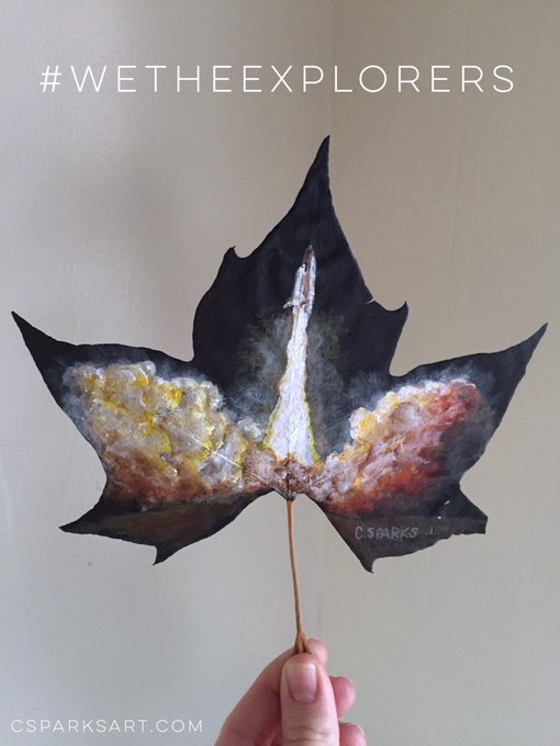
OSIRIS-REx is scheduled to launch in September and travel to the asteroid Bennu. The #WeTheExplorers campaign invites the public to take part in this mission by expressing, through art, how the mission’s spirit of exploration is reflected in their own lives. Submitted works of art will be saved on a chip on the spacecraft. The spacecraft already carries a chip with more than 442,000 names submitted through the 2014 “Messages to Bennu” campaign.

“The development of the spacecraft and instruments has been a hugely creative process, where ultimately the canvas is the machined metal and composites preparing for launch in September,” said Jason Dworkin, OSIRIS-REx project scientist at NASA’s Goddard Space Flight Center in Greenbelt, Maryland. “It is fitting that this endeavor can inspire the public to express their creativity to be carried by OSIRIS-REx into space.”

A submission may take the form of a sketch, photograph, graphic, poem, song, short video or other creative or artistic expression that reflects what it means to be an explorer. Submissions will be accepted via Twitter and Instagram until March 20, 2016. For details on how to include your submission on the mission to Bennu, go to:

http://www.asteroidmission.org/WeTheExplorers

“Space exploration is an inherently creative activity,” said Dante Lauretta, principal investigator for OSIRIS-REx at the University of Arizona, Tucson. “We are inviting the world to join us on this great adventure by placing their art work on the OSIRIS-REx spacecraft, where it will stay in space for millennia.”

The spacecraft will voyage to the near-Earth asteroid Bennu to collect a sample of at least 60 grams (2.1 ounces) and return it to Earth for study. Scientists expect Bennu may hold clues to the origin of the solar system and the source of the water and organic molecules that may have made their way to Earth.

Goddard provides overall mission management, systems engineering and safety and mission assurance for OSIRIS-REx. The University of Arizona, Tucson leads the science team and observation planning and processing. Lockheed Martin Space Systems in Denver is building the spacecraft. OSIRIS-REx is the third mission in NASA’s New Frontiers Program. NASA’s Marshall Space Flight Center in Huntsville, Alabama, manages New Frontiers for the agency’s Science Mission Directorate in Washington.

I wonder why the Egyptian mythology as in Osiris and Bennu. For those who need a refresher on the topic, here’s more from the Osiris entry on Wikipedia (Note: Links have been removed),

Osiris (/oʊˈsaɪərᵻs/, alternatively Ausir, Asiri or Ausar, among other spellings), was an Egyptian god, usually identified as the god of the afterlife, the underworld, and the dead, but more appropriately as the god of transition, resurrection, and regeneration.

Then there’s this from the Bennu entry on Wikipedia (Note: Links have been removed),

The Bennu is an ancient Egyptian deity linked with the sun, creation, and rebirth. It may have been the inspiration for the phoenix in Greek mythology.

You can find out more about Bennu, the asteriod, on its webpage, The long Strange Trip of Bennu on the NASA website (which also features a video animation), Note: A link has been removed,

… Born from the rubble of a violent collision, hurled through space for millions of years and dismembered by the gravity of planets, asteroid Bennu had a tough life in a rough neighborhood: the early solar system. …

“We are going to Bennu because we want to know what it has witnessed over the course of its evolution,” said Edward Beshore of the University of Arizona, Deputy Principal Investigator for NASA’s asteroid-sample-return mission OSIRIS-REx (Origins, Spectral Interpretation, Resource Identification, Security – Regolith Explorer). The mission will be launched toward Bennu in late 2016, arrive at the asteroid in 2018, and return a sample of Bennu’s surface to Earth in 2023.

“Bennu’s experiences will tell us more about where our solar system came from and how it evolved. Like the detectives in a crime show episode, we’ll examine bits of evidence from Bennu to understand more completely the story of the solar system, which is ultimately the story of our origin.”

As for the spacecraft, you can find out more about OSIRIS-REx here.

Getting back to the artwork, Sarah Cascone has written a Feb. 22, 2016 posting for artnet news, which features the call for submissions and some work which already been submitted (Note: Links have been removed),

The near-Earth asteroid Bennu will become the first extra-terrestrial art gallery, with the space agency inviting the public to contribute works of art that are inspired by the spirit of exploration.

The project will follow other important moments in space art history, which include work by Invader traveling aboard the International Space Station, conceptual artwork on the UKube-1 satellite, and even a bonsai tree launched into space.

Here’s a selection of the artworks being embedded in Cascone’s posting,

Daughter’s is spacebound! Fitting tribute to a pioneering, star-loving musician @OSIRISREx

For more inspiration, check out Cascone’s Feb. 22, 2016 posting.

Good luck!

NISE Net, the acronym remains the same but the name changes

NISE Net, the US Nanoscale Informal Science Education Network is winding down the nano and refocussing on STEM (science, technology, engineering, and mathematics). In short, NISE Net will now stand for National Informal STEM Education Network. Here’s more from the Jan. 7, 2016 NISE Net announcement in the January 2016 issue of the Nano Bite,

COMMUNITY NEWS

NISE Network is Transitioning to the National Informal STEM Education Network

Thank you for all the great work you have done over the past decade. It has opened up totally new possibilities for the decade ahead.

We are excited to let you know that with the completion of NSF funding for the Nanoscale Informal Science Education Network, and the soon-to-be-announced NASA [US National Aeronautics and Space Administration]-funded Space and Earth Informal STEM Education project, the NISE Network is transitioning to a new, ongoing identity as the National Informal STEM Education Network! While we’ll still be known as the NISE Net, network partners will now engage audiences across the United States in a range of STEM topics. Several new projects are already underway and others are in discussion for the future.

Current NISE Net projects include:

  • The original Nanoscale Informal Science Education Network (NISE Net), focusing on nanoscale science, engineering, and technology (funded by NSF and led by the Museum of Science, Boston)
  • Building with Biology, focusing on synthetic biology (funded by NSF and led by the Museum of Science with AAAS [American Association for the Advancement of Science], BioBuilder, and SynBerc [emphases mine])
  • Sustainability in Science Museums (funded by Walton Sustainability Solutions Initiatives and led by Arizona State University)
  • Transmedia Museum, focusing on science and society issues raised by Mary Shelley’s Frankenstein (funded by NSF and led by Arizona State University)
  • Space and Earth Informal STEM Education (funded by NASA and led by the Science Museum of Minnesota)

The “new” NISE Net will be led by the Science Museum of Minnesota in collaboration with the Museum of Science and Arizona State University. Network leadership, infrastructure, and participating organizations will include existing Network partners, and others attracted to the new topics. We will be in touch through the newsletter, blog, and website in the coming months to share more about our plans for the Network and its projects.

In the mean time, work is continuing with partners within the Nanoscale Informal Science Education Network throughout 2016, with an award end date of February 28, 2017. Although there will not be a new NanoDays 2016 kit, we encourage our partners to continue to engage audiences in nano by hosting NanoDays events in 2016 (March 26 – April 3) and in the years ahead using their existing kit materials. The Network will continue to host and update nisenet.org and the online catalog that includes 627 products of which 366 are NISE Net products (public and professional), 261 are Linked products, and 55 are Evaluation and Research reports. The Evaluation and Research team is continuing to work on final Network reports, and the Museum and Community Partnerships project has awarded 100 Explore Science physical kits to partners to create new or expanded collaborations with local community organizations to reach new underserved audiences not currently engaged in nano. These collaborative projects are taking place spring-summer 2016.

Thank you again for making this possible through your great work.

Best regards,

Larry Bell, Museum of Science
Paul Martin, Science Museum of Minnesota and
Rae Ostman, Arizona State University

As noted in previous posts, I’m quite interested in the synthetic biology focus the network has established in the last several months starting in late Spring 2015 and the mention of two (new-to-me) organizations, BioBuilder and Synberc piqued my interest.

I found this on the About the foundation page of the BioBuilder website,

What’s the best way to solve today’s health problems? Or hunger challenges? Address climate change concerns? Or keep the environment cleaner? These are big questions. And everyone can be part of the solutions. Everyone. Middle school students, teens, high school teachers.

At BioBuilder, we teach problem solving.
We bring current science to the classroom.
We engage our students to become real scientists — the problem solvers who will change the world.
At BioBuilder, we empower educators to be agents of educational reform by reconnecting teachers all across the country with their love of teaching and their own love of learning.

Synthetic biology programs living cells to tackle today’s challenges. Biofuels, safer foods, anti-malarial drugs, less toxic cancer treatment, biodegradable adhesives — all fuel young students’ imaginations. At BioBuilder, we empower students to tackle these big questions. BioBuilder’s curricula and teacher training capitalize on students’ need to know, to explore and to be part of solving real world problems. Developed by an award winning team out of MIT [Massachusetts Institute of Technology], BioBuilder is taught in schools across the country and supported by thought leaders in the STEM community.

BioBuilder proves that learning by doing works. And inspires.

As for Synberc, it is the Synthetic Biology Engineering Research Center and they has this to say about themselves on their About us page (Note: Links have been removed),

Synberc is a multi-university research center established in 2006 with a grant from the National Science Foundation (NSF) to help lay the foundation for synthetic biology Our mission is threefold:

develop the foundational understanding and technologies to build biological components and assemble them into integrated systems to accomplish many particular tasks;
train a new cadre of engineers who will specialize in engineering biology; and
engage the public about the opportunities and challenges of engineering biology.

Just as electrical engineers have made it possible for us to assemble computers from standardized parts (hard drives, memory cards, motherboards, and so on), we envision a day when biological engineers will be able to systematically assemble biological components such as sensors, signals, pathways, and logic gates in order to build bio-based systems that solve real-world problems in health, energy, and the environment.

In our work, we apply engineering principles to biology to develop tools that improve how fast — and how well — we can go through the design-test-build cycle. These include smart fermentation organisms that can sense their environment and adjust accordingly, and multiplex automated genome engineering, or MAGE, designed for large-scale programming and evolution of cells. We also pursue the discovery of applications that can lead to significant public benefit, such as synthetic artemisinin [emphasis mine], an anti-malaria drug that costs less and is more effective than the current plant-derived treatment.

The reference to ‘synthetic artemisinin’ caught my eye as I wrote an April 12, 2013 posting featuring this “… anti-malaria drug …” and the claim that the synthetic “… costs less and is more effective than the current plant-derived treatment” wasn’t quite the conclusion journalist, Brendan Borrell arrived at. Perhaps there’s been new research? If so, please let me know.

Royal Institution, science, and nanotechnology 101 and #RE_IMAGINE at the London College of Fashion

I’m featuring two upcoming events in London (UK).

Nanotechnology 101: The biggest thing you’ve never seen

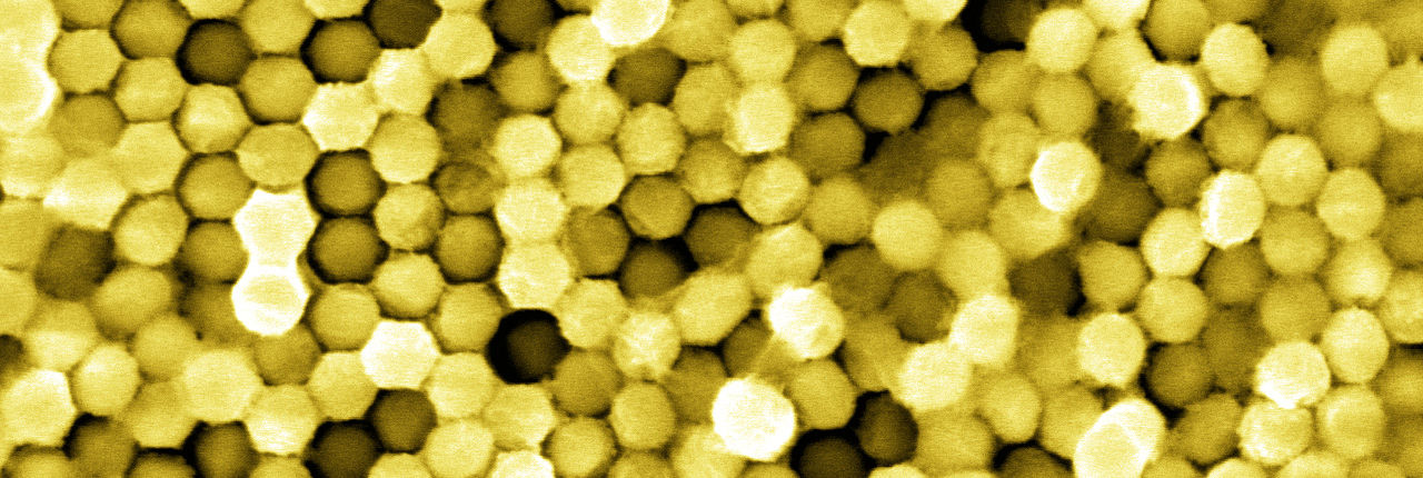
 Gold Nanowire Array Credit: lacomj via Flickr: www.flickr.com/photos/40137058@N07/3790862760

Gold Nanowire Array
Credit: lacomj via Flickr: www.flickr.com/photos/40137058@N07/3790862760 [downloaded from http://www.rigb.org/whats-on/events-2015/october/public-nanotechnology-101-the-biggest-thing-you]

Already sold out, this event is scheduled for Oct. 20, 2015. Here’s why you might want to put yourself on a waiting list, from the Royal Institution’s Nanotechnology 101 event page,

How could nanotechnology be used to create smart and extremely resilient materials? Or to boil water three times faster? Join former NASA Nanotechnology Project Manager Michael Meador to learn about the fundamentals of nanotechnology—what it is and why it’s unique—and how this emerging, disruptive technology will change the world. From invisibility cloaks to lightweight fuel-efficient vehicles and a cure for cancer, nanotechnology might just be the biggest thing you can’t see.

About the speaker

Michael Meador is currently Director of the U.S. National Nanotechnology Coordination Office, on secondment from NASA where he had been managing the Nanotechnology Project in the Game Changing Technology Program, working to mature nanotechnologies with high potential for impact on NASA missions. One part of his current job is to communicate nanotechnology research to policy-makers and the public.

Here’s some logistical information from the event page,

7.00pm to 8.30pm, Tuesday 20 October
The Theatre

Standard £12
Concession £8
Associate £6
Free to Members, Faraday Members and Fellows

For anyone who may not know offhand where the Royal Institution and its theatre is located,

The Royal Institution of Great Britain
21 Albemarle Street
London
W1S 4BS

+44 (0) 20 7409 2992
(9.00am – 6.00pm Mon – Fri)

Here’s a description of the Royal Institution from its Wikipedia entry (Note: Links have been removed),

The Royal Institution of Great Britain (often abbreviated as the Royal Institution or RI) is an organisation devoted to scientific education and research, based in London.

The Royal Institution was founded in 1799 by the leading British scientists of the age, including Henry Cavendish and its first president, George Finch, the 9th Earl of Winchilsea,[1] for

diffusing the knowledge, and facilitating the general introduction, of useful mechanical inventions and improvements; and for teaching, by courses of philosophical lectures and experiments, the application of science to the common purposes of life.
— [2]

Much of its initial funding and the initial proposal for its founding were given by the Society for Bettering the Conditions and Improving the Comforts of the Poor, under the guidance of philanthropist Sir Thomas Bernard and American-born British scientist Sir Benjamin Thompson, Count Rumford. Since its founding it has been based at 21 Albemarle Street in Mayfair. Its Royal Charter was granted in 1800. The Institution announced in January 2013 that it was considering sale of its Mayfair headquarters to meet its mounting debts.[3]

#RE_IMAGINE

While this isn’t a nanotechnology event, it does touch on topics discussed here many times: wearable technology, futuristic fashion, and the integration of technology into the body. The Digital Anthropology Lab (of the  London College of Fashion, which is part of the University of the Arts London) is being officially launched with a special event on Oct. 16, 2015. Before describing the event, here’s more about the Digital Anthropology Lab from its homepage,

Crafting fashion experience digitally

The Digital Anthropology Lab, launching in Autumn 2015, London College of Fashion, University of the Arts London is a research studio bringing industry and academia together to develop a new way of making smarter with technology.

The Digital Anthropology Lab, London College of Fashion, experiments with artefacts, communities, consumption and making in the digital space, using 3D printing, body scanning, code and electronics. We focus on an experimental approach to digital anthropology, allowing us to practically examine future ways in which digital collides with the human experience. We connect commercial partners to leading research academics and graduate students, exploring seed ideas for fashion tech.

Now

WEARABLES
We radically re-imagine this emerging fashion- tech space, exploring both the beautification of technology for wearables and critically explore the ‘why.’

Near

IoT BIG DATA
Join us to experiment with, ‘The Internet of Fashion Things.’ Where the Internet of Things, invisible big data technologies, virtual fit and meta-data collide.

Future

DESIGN FICTIONS
With the luxury of the imagination, we aim to re- wire our digital ambitions and think again about designing future digital fashion experiences for generation 2050.

Here’s information I received from the Sept. 30, 2015 announcement I received via email,

The Digital Anthropology Lab at London College of Fashion, UAL invites you to #RE_IMAGINE: A forum exploring the now, near and future of fashion technology.

#RE_IMAGINE, the Digital Anthropology Lab’s launch event, will present a fantastically diverse range of digital speakers and ask them to respond to the question – ‘Where are our digital selves heading?’

Join us to hear from pioneers, risk takers, entrepreneurs, designers and inventors including Ian Livingston CBE, Luke Robert Mason from New Bionics, Katie Baron from Stylus, J. Meejin Yoon from MIT among others. Also come to see what happened when we made fashion collide with the Internet of Things, they are wearable but not as you know it…

#RE_IMAGINE aims to be an informative, networked and enlightening brainstorm of a day. To book your place please follow this link.

To coincide with the exhibition Digital Disturbances, Fashion Space Gallery presents a late night opening event. Alongside a curator tour will be a series of interactive demonstrations and displays which bring together practitioners working across design, science and technology to investigate possible human and material futures. We’d encourage you to stay and enjoy this networking opportunity.

Friday 16th October 2015

9.30am – 5pm – Forum event 

5pm – 8.30pm – Digital Disturbances networking event

London College of Fashion

20 John Princes Street
London
W1G 0BJ 

Ticket prices are £75.00 for a standard ticket and £35.00 for concession tickets (more details here).

For more #RE_IMAGINE specifics, there’s the event’s Agenda page. As for Digital Disturbances, here’s more from the Fashion Space Gallery’s Exhibition homepage,

Digital Disturbances

11th September – 12th December 2015

Digital Disturbances examines the influence of digital concepts and tools on fashion. It provides a lens onto the often strange effects that emerge from interactions across material and virtual platforms – information both lost and gained in the process of translation. It presents the work of seven designers and creative teams whose work documents these interactions and effects, both in the design and representation of fashion. They can be traced across the surfaces of garments, through the realisation of new silhouettes, in the remixing of images and bodies in photography and film, and into the nuances of identity projected into social and commercial spaces.

Designers include: ANREALAGE, Bart Hess, POSTmatter, Simone C. Niquille and Alexander Porter, Flora Miranda, Texturall and Tigran Avetisyan.

Digital Disturbances is curated by Leanne Wierzba.

Two events—two peeks into the future.

D-Wave upgrades Google’s quantum computing capabilities

Vancouver-based (more accurately, Burnaby-based) D-Wave systems has scored a coup as key customers have upgraded from a 512-qubit system to a system with over 1,000 qubits. (The technical breakthrough and concomitant interest from the business community was mentioned here in a June 26, 2015 posting.) As for the latest business breakthrough, here’s more from a Sept. 28, 2015 D-Wave press release,

D-Wave Systems Inc., the world’s first quantum computing company, announced that it has entered into a new agreement covering the installation of a succession of D-Wave systems located at NASA’s Ames Research Center in Moffett Field, California. This agreement supports collaboration among Google, NASA and USRA (Universities Space Research Association) that is dedicated to studying how quantum computing can advance artificial intelligence and machine learning, and the solution of difficult optimization problems. The new agreement enables Google and its partners to keep their D-Wave system at the state-of-the-art for up to seven years, with new generations of D-Wave systems to be installed at NASA Ames as they become available.

“The new agreement is the largest order in D-Wave’s history, and indicative of the importance of quantum computing in its evolution toward solving problems that are difficult for even the largest supercomputers,” said D-Wave CEO Vern Brownell. “We highly value the commitment that our partners have made to D-Wave and our technology, and are excited about the potential use of our systems for machine learning and complex optimization problems.”

Cade Wetz’s Sept. 28, 2015 article for Wired magazine provides some interesting observations about D-Wave computers along with some explanations of quantum computing (Note: Links have been removed),

Though the D-Wave machine is less powerful than many scientists hope quantum computers will one day be, the leap to 1000 qubits represents an exponential improvement in what the machine is capable of. What is it capable of? Google and its partners are still trying to figure that out. But Google has said it’s confident there are situations where the D-Wave can outperform today’s non-quantum machines, and scientists at the University of Southern California [USC] have published research suggesting that the D-Wave exhibits behavior beyond classical physics.

A quantum computer operates according to the principles of quantum mechanics, the physics of very small things, such as electrons and photons. In a classical computer, a transistor stores a single “bit” of information. If the transistor is “on,” it holds a 1, and if it’s “off,” it holds a 0. But in quantum computer, thanks to what’s called the superposition principle, information is held in a quantum system that can exist in two states at the same time. This “qubit” can store a 0 and 1 simultaneously.

Two qubits, then, can hold four values at any given time (00, 01, 10, and 11). And as you keep increasing the number of qubits, you exponentially increase the power of the system. The problem is that building a qubit is a extreme difficult thing. If you read information from a quantum system, it “decoheres.” Basically, it turns into a classical bit that houses only a single value.

D-Wave claims to have a found a solution to the decoherence problem and that appears to be borne out by the USC researchers. Still, it isn’t a general quantum computer (from Wetz’s article),

… researchers at USC say that the system appears to display a phenomenon called “quantum annealing” that suggests it’s truly operating in the quantum realm. Regardless, the D-Wave is not a general quantum computer—that is, it’s not a computer for just any task. But D-Wave says the machine is well-suited to “optimization” problems, where you’re facing many, many different ways forward and must pick the best option, and to machine learning, where computers teach themselves tasks by analyzing large amount of data.

It takes a lot of innovation before you make big strides forward and I think D-Wave is to be congratulated on producing what is to my knowledge the only commercially available form of quantum computing of any sort in the world.

ETA Oct. 6, 2015* at 1230 hours PST: Minutes after publishing about D-Wave I came across this item (h/t Quirks & Quarks twitter) about Australian researchers and their quantum computing breakthrough. From an Oct. 6, 2015 article by Hannah Francis for the Sydney (Australia) Morning Herald,

For decades scientists have been trying to turn quantum computing — which allows for multiple calculations to happen at once, making it immeasurably faster than standard computing — into a practical reality rather than a moonshot theory. Until now, they have largely relied on “exotic” materials to construct quantum computers, making them unsuitable for commercial production.

But researchers at the University of New South Wales have patented a new design, published in the scientific journal Nature on Tuesday, created specifically with computer industry manufacturing standards in mind and using affordable silicon, which is found in regular computer chips like those we use every day in smartphones or tablets.

“Our team at UNSW has just cleared a major hurdle to making quantum computing a reality,” the director of the university’s Australian National Fabrication Facility, Andrew Dzurak, the project’s leader, said.

“As well as demonstrating the first quantum logic gate in silicon, we’ve also designed and patented a way to scale this technology to millions of qubits using standard industrial manufacturing techniques to build the world’s first quantum processor chip.”

According to the article, the university is looking for industrial partners to help them exploit this breakthrough. Fisher’s article features an embedded video, as well as, more detail.

*It was Oct. 6, 2015 in Australia but Oct. 5, 2015 my side of the international date line.

ETA Oct. 6, 2015 (my side of the international date line): An Oct. 5, 2015 University of New South Wales news release on EurekAlert provides additional details.

Here’s a link to and a citation for the paper,

A two-qubit logic gate in silicon by M. Veldhorst, C. H. Yang, J. C. C. Hwang, W. Huang,    J. P. Dehollain, J. T. Muhonen, S. Simmons, A. Laucht, F. E. Hudson, K. M. Itoh, A. Morello    & A. S. Dzurak. Nature (2015 doi:10.1038/nature15263 Published online 05 October 2015

This paper is behind a paywall.

3D imaging biological cells with picosecond ultrasonics (acoustic imaging)

An April 22, 2015 news item on Nanowerk describes an acoustic imaging technique that’s been newly applied to biological cells,

Much like magnetic resonance imaging (MRI) is able to scan the interior of the human body, the emerging technique of “picosecond ultrasonics,” a type of acoustic imaging, can be used to make virtual slices of biological tissues without destroying them.

Now a team of researchers in Japan and Thailand has shown that picosecond ultrasonics can achieve micron resolution of single cells, imaging their interiors in slices separated by 150 nanometers — in stark contrast to the typical 0.5-millimeter spatial resolution of a standard medical MRI scan. This work is a proof-of-principle that may open the door to new ways of studying the physical properties of living cells by imaging them in vivo.

An April 20, 2015 American Institute of Physics news release, which originated the news item, provides a description of picosecond ultrasonics and more details about the research,

Picosecond ultrasonics has been used for decades as a method to explore the mechanical and thermal properties of materials like metals and semiconductors at submicron scales, and in recent years it has been applied to biological systems as well. The technique is suited for biology because it’s sensitive to sound velocity, density, acoustic impedance and the bulk modulus of cells.

This week, in a story appearing on the cover of the journal Applied Physics Letters, from AIP Publishing, researchers from Walailak University in Thailand and Hokkaido University in Japan describe the first known demonstration of 3-D cell imaging using picosecond ultrasonics.

Their work centers on imaging two types of mammalian biological tissue — a bovine aortic endothelial cell, a type of cell that lines a cow’s main artery blood vessel, and a mouse “adipose” fat cell. Endothelial cells were chosen because they play a key role in the physiology of blood cells and are useful in the study of biomechanics. Fat cells, on the other hand, were studied to provide an interesting comparison with varying cell geometries and contents.

How the Work was Done

The team accomplished the imaging by first placing a cell in solution on a titanium-coated sapphire substrate and then scanning a point source of high-frequency sound generated by using a beam of focused ultrashort laser pulses over the titanium film. This was followed by focusing another beam of laser pulses on the same point to pick up tiny changes in optical reflectance caused by the sound traveling through the cell tissue.

“By scanning both beams together, we’re able to build up an acoustic image of the cell that represents one slice of it,” explained co-author Professor Oliver B. Wright, who teaches in the Division of Applied Physics, Faculty of Engineering at Hokkaido University. “We can view a selected slice of the cell at a given depth by changing the timing between the two beams of laser pulses.”

The team’s work is particularly noteworthy because “in spite of much work imaging cells with more conventional acoustic microscopes, the time required for 3-D imaging probably remains too long to be practical,” Wright said. “Building up a 3-D acoustic image, in principle, allows you to see the 3-D relative positions of cell organelles without killing the cell. In our experiments in vitro, while we haven’t yet resolved the cell contents — possibly because cell nuclei weren’t contained within the slices we viewed — it should be possible in the future with various improvements to the technique.”

: Fluorescence micrographs of fat and endothelial cells superimposed on differential-interference and phase-contrast images, respectively.

Fluorescence micrographs of fat and endothelial cells superimposed on differential-interference and phase-contrast images, respectively. The nuclei are stained blue in the micrographs. The image on the right is a picosecond-ultrasonic image of a single endothelial cell with approximately 1-micron lateral and 150-nanometer depth resolutions. Deep blue corresponds to the lowest ultrasonic amplitude.
CREDIT: O. Wright/Hokkaido University

So far, the team has used infrared light to generate sound waves within the cell, “limiting the lateral spatial resolution to about one micron,” Wright explains. “By using an ultraviolet-pulsed laser, we could improve the lateral resolution by about a factor of three — and greatly improve the image quality. And, switching to a diamond substrate instead of sapphire would allow better heat conduction away from the probed area, which, in turn, would enable us to increase the laser power and image quality.”

So lowering the laser power or using substrates with higher thermal conductivity may soon open the door to in vivo imaging, which would be invaluable for investigating the mechanical properties of cell organelles within both vegetal and animal cells.

What’s next for the team? “The method we use to image the cells now actually involves a combination of optical and elastic parameters of the cell, which can’t be easily distinguished,” Wright said. “But we’ve thought of a way to separate them, which will allow us to measure the cell mechanical properties more accurately. So we’ll try this method in the near future, and we’d also like to try our method on single-celled organisms or even bacteria.”

Here’s a link to and a citation for the paper,

Three-dimensional imaging of biological cells with picosecond ultrasonics by Sorasak Danworaphong, Motonobu Tomoda, Yuki Matsumoto, Osamu Matsuda, Toshiro Ohashi, Hiromu Watanabe, Masafumi Nagayama, Kazutoshi Gohara, Paul H. Otsuka, and Oliver B. Wright. Appl. Phys. Lett. 106, 163701 (2015); http://dx.doi.org/10.1063/1.4918275

This paper is open access.

This research reminded me of a data sonification project that I featured in a Feb. 7, 2014 post which includes an embedded sound file of symphonic music based on data from NASA’s (US National Aeronautics and Space Administration) Voyager spacecraft.

Carbon nanotube commercialization report from the US National Nanotechnology Initiative

Apparently a workshop on the topic commercializing carbon nanotubes was held in Washington, DC. in Sept. 2014. A March 12, 2015 news item on Nanowerk (originated by  March 12, 2015 US National Nanotechnology Initiative news release on EurekAlert) announces the outcome of that workshop (Note: Links have been removed),

The National Nanotechnology Initiative today published the proceedings of a technical interchange meeting on “Realizing the Promise of Carbon Nanotubes: Challenges, Opportunities, and the Pathway to Commercialization” (pdf), held at the National Aeronautics and Space Administration (NASA) Headquarters on September 15, 2014. This meeting brought together some of the Nation’s leading experts in carbon nanotube materials to identify, discuss, and report on technical barriers to the production of carbon nanotube (CNT)-based bulk and composite materials with properties that more closely match those of individual CNTs and to explore ways to overcome these barriers.

The outcomes of this meeting, as detailed in this report, will help inform the future directions of the NNI Nanotechnology Signature Initiative “Sustainable Nanomanufacturing: Creating the Industries of the Future”, which was launched in 2010 to accelerate the development of industrial-scale methods for manufacturing functional nanoscale systems.

The Technical Interchange Proceedings ‘Realizing the Promise of Carbon Nanotubes: Challenges, Opportunities, and the Pathway to Commercialization‘ (30 pp. PDF) describes areas for improvement in its executive summary,

A number of common themes and areas requiring focused attention were identified:

● Increased efforts devoted to manufacturing, quality control, and scale-up are needed. The development of a robust supply of CNT bulk materials with well-controlled properties would greatly enhance commercialization and spur use in a broad range of applications.
● Improvements are needed in the mechanical and electrical properties of CNT-based bulk materials (composites, sheets, and fibers) to approach the properties of individual CNTs. The development of bulk materials with properties nearing ideal CNT values would accelerate widespread adoption of these materials.
● More effective use of simulation and modeling is needed to provide insight into the fundamentals of the CNT growth process. Theoretical insight into the fundamentals of the growth process will inform the development of processes capable of producing high-quality material in quantity.
● Work is needed to help develop an understanding of the properties of bulk CNT-containing materials at longer length scales. Longer length scale understanding will enable the development of predictive models of structure–process–properties relationships and structural design technology tailored to take advantage of CNT properties.
● Standard materials and protocols are needed to guide the testing of CNT-based products for commercial applications. Advances in measurement methods are also required to characterize bulk CNT material properties and to understand the mechanism(s) of failure to help ensure material reliability.
● Life cycle assessments are needed for gauging commercial readiness. Life cycle assessments should include energy usage, performance lifetime, and degradation or disposal of CNT-based products.
● Collaboration to leverage resources and expertise is needed to advance commercialization of CNT-based products. Coordinated, focused efforts across academia, government laboratories, and industry to target grand challenges with support from public–private partnerships would accelerate efforts to provide solutions to overcome these technical barriers.

This meeting identified a number of the technical barriers that need to be overcome to make the promise of carbon nanotubes a reality. A more concerted effort is needed to focus R&D activities towards addressing these barriers and accelerating commercialization. The outcomes from this meeting will inform the future directions of the NNI Nanomanufacturing Signature Initiative and provide specific areas that warrant broader focus in the CNT research community. [p. vii print; p. 9 PDF]

This report, in its final section, explains the basis for the interest in and the hopes for carbon nanotubes,

Improving the electrical and mechanical properties of bulk carbon nanotube materials (yarns, fibers, wires, sheets, and composites) to more closely match those of individual carbon nanotubes will enable a revolution in materials that will have a broad impact on U.S. industries, global competitiveness, and the environment. Use of composites reinforced with high-strength carbon nanotube fibers in terrestrial and air transportation vehicles could enable a 25% reduction in their overall weight, reduce U.S. oil consumption by nearly 6 million barrels per day by 2035 [42], and reduce worldwide consumption of petroleum and other liquid fuels by 25%. This would result in the reduction of CO2 emissions by as much as 3.75 billion metric tons per year. Use of carbon nanotube-based data and power cables would lead to further reductions in vehicle weight, fuel consumption, and CO2 emissions. For example, replacement of the copper wiring in a Boeing 777 with CNT data and power cables that are 50% lighter would enable a 2,000-pound reduction in airplane weight. Use of carbon nanotube wiring in power distribution lines would reduce transmission losses by approximately 41 billion kilowatt hours annually [42], leading to significant savings in coal and gas consumption and reductions in the electric power industry’s carbon footprint.

The impact of developing these materials on U.S. global competitiveness is also significant. For example, global demand for carbon fibers is expected to grow from 46,000 metric tons per year in 2011 to more than 153,000 metric tons in 2020 due to the exponential growth in the use of composites in commercial aircraft, automobiles, aerospace, and wind energy [43]. Ultrahigh-strength CNT fibers would be highly attractive in each of these applications because they offer the advantage of reduced weight and improved performance over conventional carbon fibers. [p. 10 print; p. 20 PDF]

As these things go, this is a very short document, which makes it a fast read, and it has a reference list, something I always find useful.

My colleague, Dexter Johnson in a March 17, 2015 posting on his Nanoclast blog (on the IEEE [Institute for Electrical and Electronics Engineers] website) provides some background information before launching into an analysis of the report’s recommendations (Note: Links have been removed),

In the last half-a-decade we have witnessed once-beloved carbon nanotubes (CNTs) slowly being eclipsed by graphene as the “wonder material” of the nanomaterial universe.

This changing of the guard has occurred primarily within the research community, where the amount of papers being published about graphene seems to be steadily increasing. But in terms of commercial development, CNTs still have a leg up on graphene, finding increasing use in creating light but strong composites. Nonetheless, the commercial prospects for CNTs have been taking hits recently, with some producers scaling down capacity because of lack of demand.

With this as the backdrop, the National Nanotechnology Initiative (NNI), famous for its estimate back in 2001 that the market for nanotechnology will be worth $1 trillion by 2015,  has released a report based on a meeting held last September. …

I recommend reading Dexter’s analysis.

Outer space telescopes made of micro- and nanoparticles (smart dust)

Scientists at Rochester Institute of Technology (RIT is located in New York state) are working on a project that would see ‘smart dust’ used as a telescope in outer space. From a Dec. 1, 2014 news item on phys.org,

Telescope lenses someday might come in aerosol cans. Scientists at Rochester Institute of Technology and the NASA [ National Aeronautics and Space Administration] Jet Propulsion Laboratory are exploring a new type of space telescope with an aperture made of swarms of particles released from a canister and controlled by a laser.

These floating lenses would be larger, cheaper and lighter than apertures on conventional space-based imaging systems like NASA’s Hubble and James Webb space telescopes, said Grover Swartzlander, associate professor at RIT’s Chester F. Carlson Center for Imaging Science and Fellow of the Optical Society of America. Swartzlander is a co-investigator on the Jet Propulsion team led by Marco Quadrelli.

A Dec. 1, 2014 RIT news release by Susan Gawlowicz, which originated the news item, describes the NASA project and provides more details about the technology,

NASA’s Innovative Advanced Concepts Program is funding the second phase of the “orbiting rainbows” project that attempts to combine space optics and “smart dust,” or autonomous robotic system technology. The smart dust is made of a photo-polymer, or a light-sensitive plastic, covered with a metallic coating.

“Our motivation is to make a very large aperture telescope in space and that’s typically very expensive and difficult to do,” Swartzlander said. “You don’t have to have one continuous mass telescope in order to do astronomy—it can be distributed over a wide distance. Our proposed concept could be a very cheap, easy way to achieve large coverage, something you couldn’t do with the James Webb-type of approach.”

An adaptive optical imaging sensor comprised of tiny floating mirrors could support large-scale NASA missions and lead to new technology in astrophysical imaging and remote sensing.

Swarms of smart dust forming single or multiple lenses could grow to reach tens of meters to thousands of kilometers in diameter. According to Swartzlander, the unprecedented resolution and detail might be great enough to spot clouds on exoplanets, or planets beyond our solar system.

“This is really next generation,” Swartzlander said. “It’s 20, 30 years out. We’re at the very first step.”

Previous scientists have envisioned orbiting apertures but not the control mechanism. This new concept relies upon Swartzlander’s expertise in the use of light, or photons, to manipulate micro- or nano-particles like smart dust. He developed and patented the techniques known as “optical lift,” in which light from a laser produces radiation pressure that controls the position and orientation of small objects.

In this application, radiation pressure positions the smart dust in a coherent pattern oriented toward an astronomical object. The reflective particles form a lens and channel light to a sensor, or a large array of detectors, on a satellite. Controlling the smart dust to reflect enough light to the sensor to make it work will be a technological hurdle, Swartzlander said.

Two RIT graduate students on Swartzlander’s team are working on different aspects of the project. Alexandra Artusio-Glimpse, a doctoral student in imaging science, is designing experiments in low-gravity environments to explore techniques for controlling swarms of particle and to determine the merits of using a single or multiple beams of light.

Swartzlander expects the telescope will produce speckled and grainy images. Xiaopeng Peng, a doctoral student in imaging science, is developing software algorithms for extracting information from the blurred image the sensor captures. The laser that will shape the smart dust into a lens also will measure the optical distortion caused by the imaging system. Peng will use this information to develop advanced image processing techniques to reverse the distortion and recover detailed images.

“Our goal at this point is to marry advanced computational photography with radiation-pressure control techniques to achieve a rough image,” Swartzlander said. “Then we can establish a roadmap for improving both the algorithms and the control system to achieve ‘out of this world’ images.”

You can find out more about NASA’s Orbiting Rainbows project here.

I just mentioned rainbows and optics with regard to Robert Grosseteste, a 13th century cleric who ‘unwove’ rainbows, in a Dec. 1, 2014 posting (scroll down about 60% of the way).

NASA, super-black nanotechnology, and an International Space Station livestreamed event

A super-black nanotechnology-enabled coating (first mentioned here in a July 18, 2013 posting featuring work by John Hagopian, an optics engineer at the US National Aeronautics and Space Administration [NASA’s] Goddard Space Flight Center on this project) is about to be tested in outer space. From an Oct. 23, 2014 news item on Nanowerk,

An emerging super-black nanotechnology that is to be tested for the first time this fall on the International Space Station will be applied to a complex, 3-D component critical for suppressing stray light in a new, smaller, less-expensive solar coronagraph designed to ultimately fly on the orbiting outpost or as a hosted payload on a commercial satellite.

The super-black carbon-nanotube coating, whose development is six years in the making, is a thin, highly uniform coating of multi-walled nanotubes made of pure carbon about 10,000 times thinner than a strand of human hair. Recently delivered to the International Space Station for testing, the coating is considered especially promising as a technology to reduce stray light, which can overwhelm faint signals that sensitive detectors are supposed to retrieve.

An Oct. 24, 2014 NASA news release by Lori Keesey, which originated the news item, further describes the work being done on the ground simultaneous to the tests on the International Space Station,

While the coating undergoes testing to determine its robustness in space, a team at NASA’s Goddard Space Flight Center in Greenbelt, Maryland, will apply the carbon-nanotube coating to a complex, cylindrically shaped baffle — a component that helps reduce stray light in telescopes.

Goddard optical engineer Qian Gong designed the baffle for a compact solar coronagraph that Principal Investigator Nat Gopalswamy is now developing. The goal is [to] build a solar coronagraph that could deploy on the International Space Station or as a hosted payload on a commercial satellite — a much-needed capability that could guarantee the continuation of important space weather-related measurements.

The effort will help determine whether the carbon nanotubes are as effective as black paint, the current state-of-the-art technology, for absorbing stray light in complex space instruments and components.

Preventing errant light is an especially tricky challenge for Gopalswamy’s team. “We have to have the right optical system and the best baffles going,” said Doug Rabin, a Goddard heliophysicist who studies diffraction and stray light in coronagraphs.

The new compact coronagraph — designed to reduce the mass, volume, and cost of traditional coronagraphs by about 50 percent — will use a single set of lenses, rather than a conventional three-stage system, to image the solar corona, and more particularly, coronal mass ejections (CMEs). These powerful bursts of solar material erupt and hurdle across the solar system, sometimes colliding with Earth’s protective magnetosphere and posing significant hazards to spacecraft and astronauts.

“Compact coronagraphs make greater demands on controlling stray light and diffraction,” Rabin explained, adding that the corona is a million times fainter than the sun’s photosphere. Coating the baffle or occulter with the carbon-nanotube material should improve the component’s overall performance by preventing stray light from reaching the focal plane and contaminating measurements.

The project is well timed and much needed, Rabin added.

Currently, the heliophysics community receives coronagraphic measurements from the Solar and Heliospheric Observatory (SOHO) and the Solar Terrestrial Relations Observatory (STEREO).

“SOHO, which we launched in 1995, is one of our Great Observatories,” Rabin said. “But it won’t last forever.” Although somewhat newer, STEREO has operated in space since 2006. “If one of these systems fails, it will affect a lot of people inside and outside NASA, who study the sun and forecast space weather. Right now, we have no scheduled mission that will carry a solar coronagraph. We would like to get a compact coronagraph up there as soon as possible,” Rabin added.

Ground-based laboratory testing indicates it could be a good fit. Testing has proven that the coating absorbs 99.5 percent of the light in the ultraviolet and visible and 99.8 percent in the longer infrared bands due to the fact that the carbon atoms occupying the tiny nested tubes absorb the light and prevent it from reflecting off surfaces, said Goddard optics engineer John Hagopian, who is leading the technology’s advancement. Because only a tiny fraction of light reflects off the coating, the human eye and sensitive detectors see the material as black — in this case, extremely black.

“We’ve made great progress on the coating,” Hagopian said. “The fact the coatings have survived the trip to the space station already has raised the maturity of the technology to a level that qualifies them for flight use. In many ways the external exposure of the samples on the space station subjects them to a much harsher environment than components will ever see inside of an instrument.”

Given the need for a compact solar coronagraph, Hagopian said he’s especially excited about working with the instrument team. “This is an important instrument-development effort, and, of course, one that could showcase the effectiveness of our technology on 3-D parts,” he said, adding that the lion’s share of his work so far has concentrated on 2-D applications.

By teaming with Goddard technologist Vivek Dwivedi, Hagopian believes the baffle project now is within reach. Dwivedi is advancing a technique called atomic layer deposition (ALD) that lays down a catalyst layer necessary for carbon-nanotube growth on complex, 3-D parts. “Previous ALD chambers could only hold objects a few millimeters high, while the chamber Vivek has developed for us can accommodate objects 20 times bigger; a necessary step for baffles of this type,” Hagopian said.

Other NASA researchers have flown carbon nanotubes on the space station, but their samples were designed for structural applications, not stray-light suppression — a completely different use requiring that the material demonstrate greater absorption properties, Hagopian said.

“We have extreme stray light requirements. Let’s see how this turns out,” Rabin said.

The researchers from NASA have kindly made available an image of a baffle prior to receiving its super-black coating,

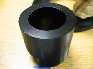
This is a close-up view of a baffle that will be coated with a carbon-nanotube coating. Image Credit:  NASA Goddard/Paul Nikulla

This is a close-up view of a baffle that will be coated with a carbon-nanotube coating.
Image Credit: NASA Goddard/Paul Nikulla

There’s more information about the project in this August 12, 2014 NASA news release first announcing the upcoming test.

Serendipitously or not, NASA is hosting an interactive Space Technology Forum on Oct. 27, 2014 (this coming Monday) focusing on technologies being demonstrated on the International Space Station (ISS) according to an Oct. 20, 2014 NASA media advisory,

Media are invited to interact with NASA experts who will answer questions about technologies being demonstrated on the International Space Station (ISS) during “Destination Station: ISS Technology Forum” from 10 to 11 a.m. EDT (9 to 10 a.m. CDT [7 to 8 am PDT]) Monday, Oct. 27, at the U.S. Space & Rocket Center in Huntsville, Alabama.

The forum will be broadcast live on NASA Television and the agency’s website.

The Destination Station forums are a series of live, interactive panel discussions about the space station. This is the second in the series, and it will feature a discussion on how technologies are tested aboard the orbiting laboratory. Thousands of investigations have been performed on the space station, and although they provide benefits to people on Earth, they also prepare NASA to send humans farther into the solar system than ever before.

Forum panelists and exhibits will focus on space station environmental and life support systems; 3-D printing; Space Communications and Navigation (SCaN) systems; and Synchronized Position Hold, Engage, Reorient, Experimental Satellites (SPHERES).

The forum’s panelists are:
– Jeffrey Sheehy, senior technologist in NASA’s Space Technology Mission Directorate
– Robyn Gatens, manager for space station System and Technology Demonstration, and Environmental Control Life Support System expert
– Jose Benavides, SPHERES chief engineer
– Rich Reinhart, principal investigator for the SCaN Testbed
– Niki Werkeiser, project manager for the space station 3-D printer

During the forum, questions will be taken from the audience, including media, students and social media participants. Online followers may submit questions via social media using the hashtag, #asknasa. [emphasis mine] …

The “Destination Station: ISS Technology Forum” coincides with the 7th Annual Von Braun Memorial Symposium at the University of Alabama in Huntsville Oct. 27-29. Media can attend the three-day symposium, which features NASA officials, including NASA Administrator Charles Bolden, Associate Administrator for Human Exploration and Operation William Gerstenmaier and Assistant Deputy Associate Administrator for Exploration Systems Development Bill Hill. Jean-Jacques Dordain, director general of the European Space Agency, will be a special guest speaker. Representatives from industry and academia also will be participating.

For NASA TV streaming video, scheduling and downlink information, visit:

http://www.nasa.gov/nasatv

For more information on the International Space Station and its crews, visit:

http://www.nasa.gov/station

I have checked out the livestreaming/tv site and it appears that registration is not required for access. Sadly, I don’t see any the ‘super-black’ coating team members mentioned in the news release on the list of forum participants.

ETA Oct. 27, 2014: You can check out Dexter Johnson’s Oct. 24, 2014 posting on the Nanoclast blog (on the IEEE [Institute of Electrical and Electronics Engineers] website for a little more information