A Feb. 24, 2015 news item on Nanowerk describes nanoantenna research coming out of Australia (Note: A link has been removed),
Newly developed tiny antennas, likened to spotlights on the nanoscale, offer the potential to measure food safety, identify pollutants in the air and even quickly diagnose and treat cancer, according to the Australian scientists who created them. The new antennas are cubic in shape. They do a better job than previous spherical ones at directing an ultra-narrow beam of light where it is needed, with little or no loss due to heating and scattering, they say.
In a paper published in the Journal of Applied Physics (“Optically resonant magneto-electric cubic nanoantennas for ultra-directional light scattering”), Debabrata Sikdar of Monash University in Victoria, Australia, and colleagues describe these and other envisioned applications for their nanocubes in “laboratories-on-a-chip.” …
… The cubes, composed of insulating, rather than conducting or semiconducting materials as were the spherical versions, are easier to fabricate as well as more effective, he [Sikdar] says.
Sikdar’s paper presents analysis and simulation of 200-nanometer dielectric (nonconductive) nanoncubes placed in the path of visible and near-infrared light sources. The nanocubes are arranged in a chain, and the space between them can be adjusted to fine-tune the light beam as needed for various applications. As the separation between cubes increases, the angular width of the beam narrows and directionality improves, the researchers say.
“Unidirectional nanoantennas induce directionality to any omnidirectional light emitters like microlasers, nanolasers or spasers, and even quantum dots,” Sikdar said in an interview. Spasers are similar to lasers, but employ minute oscillations of electrons rather than light. Quantum dots are tiny crystals that produce specific colors, based on their size, and are widely used in color televisions. “Analogous to nanoscale spotlights, the cubic antennas focus light with precise control over direction and beam width,” he said. [emphasis mine]
The new cubic nanoantennas have the potential to revolutionize the infant field of nano-electromechanical systems (NEMS). “These unidirectional nanoantennas are most suitable for integrated optics-based biosensors to detect proteins, DNA, antibodies, enzymes, etc., in truly portable lab-on-a-chip platforms of the future,” Sikdar said. “They can also potentially replace the lossy on-chip IC (integrated circuit) interconnects, via transmitting optical signals within and among ICs, to ensure ultrafast data processing while minimizing device heating,” he added. [emphasis mine]
Sikdar and his colleagues plan to begin constructing unidirectional cubic NEMS antennas in the near future at the Melbourne Center for Nanofabrication. “We would like to collaborate with other research groups across the world, making all these wonders possible,” he said.
I’m glad the writer included Sikdar’s explanation of spasers and quantum dots and thank them both for a new word, “lossy.” Here’s a link to and a citation for the paper,
There’s a very interesting Jan. 8, 2015 essay by Dr. Andrew Maynard, being hosted on Nanowerk, about the effects that quantum dot televisions could have on the environment (Note: A link has been removed),
Earlier this week, The Conversation reported that, “The future is bright, the future is … quantum dot televisions”. And judging by the buzz coming from this week’s annual Consumer Electronics Show (CES) that’s right – the technology is providing manufacturers with a cheap and efficient way of producing the next generation of brilliant, high-definition TV screens.
But the quantum dots in these displays also use materials and technologies – including engineered nanoparticles and the heavy metal cadmium – that have been a magnet for health and environmental concerns. Will the dazzling pictures this technology allow blind us to new health and environmental challenges, or do their benefits outweigh the potential risks?
If I understand things rightly, cadmium is toxic at both the macroscale and the nanoscale and Andrew goes on to describe quantum dots (cadmium at the nanoscale) and the problem they could present in his Jan. 7, 2015 essay on The Conversation,also hosted by Nanowerk, (Note: Link have been removed),
Quantum dots are a product of the emerging field of nanotechnology. They are made of nanometer-sized particles of a semiconducting material – often cadmium selenide. About 2,000 to 20,000 times smaller than the width of a single human hair, they’re designed to absorb light of one color and emit it as another color – to fluoresce. This property makes them particularly well-suited for use in products like tablets and TVs that need bright, white, uniform backlights.
… What is unique about quantum dots is that the color of the emitted light can be modified by simply changing the size of the quantum dot particles. And because this color-shifting is a physical phenomenon, quantum dots far outperform their chemical counterparts in brightness, color and durability.
Unfortunately, the heavy metal cadmium used in the production of many quantum dots is a health and environmental hazard.
…
On top of this, the potential health and environmental impacts of engineered nanoparticles like quantum dots have been raising concerns with toxicologists and regulators for over a decade now. Research has shown that the size, shape and surface properties of some particles influence the harm they are capable of causing in humans and the environment; smaller particles are often more toxic than their larger counterparts. That said, this is an area where scientific understanding is still developing.
Together, these factors would suggest caution is warranted in adopting quantum dot technologies. Yet taken in isolation they are misleading.
The essay describes the risk factors for various sectors (Note: A link has been removed),
The quantum dots currently being used in TVs are firmly embedded in the screens – usually enclosed behind multiple layers of glass and plastic. As a result, the chances of users being exposed to them during normal operation are pretty much nil.
The situation is potentially different during manufacturing, when there is a chance that someone could be inadvertently exposed to these nanoscopic particles. Scenarios like this have led to agencies like the US National Institute for Occupational Safety and Health taking a close look at safety when working with nanoparticles. While the potential risks are not negligible, good working practices are effective at reducing or eliminating potentially harmful exposures.
End-of-life disposal raises additional concerns. While the nanoparticles are likely to remain firmly embedded within a trashed TV’s screen, the toxic materials they contain, including cadmium, could well be released into the environment. Cadmium is certainly a health and environmental issue with poorly regulated e-waste disposal and recycling. However, when appropriate procedures are used, exposures should be negligible.
It seems quantum dot televisions impose a smaller burden than their cousins on the environment,
Although it seems counter-intuitive, analysis by the company that was made available to the EPA [US Environmental Protection Agency] showed QD Vision’s products lead to a net decrease in environmental cadmium releases compared to conventional TVs. Cadmium is one of the pollutants emitted from coal-fired electrical power plants. Because TVs using the company’s quantum dots use substantially less power than their non-quantum counterparts, the combined cadmium in QD Vision TVs and the power plant emissions associated with their use is actually lower than that associated with conventional flat screen TVs. In other words, using cadmium in quantum dots for production of more energy-efficient displays can actually results in a net reduction in cadmium emissions.
A research team at the Okinawa Institute of Science and Technology Graduate University (OIST) in Japan has developed and patented a new more precise production technique for nanoparticles, specifically quantum dots. From a Jan. 5, 2014 news item on Nanowerk, (Note: A link has been removed),
The Nanoparticles by Design Unit at the Okinawa Institute of Science and Technology Graduate University is constantly finding new ways to endow the tiniest of particles with more specific properties. They have developed methods to control the size and chemical composition of nanoparticles, and now they have found a way to control the degree of crystallinity, or the way that atoms align inside the nanoparticles. A nanoparticle’s crystallinity impacts its optical, magnetic, and electrical properties. Professor Mukhles Sowwan and the researchers in his unit Dr. Cathal Cassidy and Vidyadhar Singh have applied for a patent for their method, which describes exactly how to create semiconductor nanoparticles of varying crystallinity.
“Most scientists and even companies nowadays are using nanoparticles not optimized for their applications or devices,” explains Sowwan. “We hope, at a certain time, we will optimize the nanoparticles for specific applications.” To start though, the researchers in the Nanoparticles by Design Unit must figure out how to control a few basic characteristics of nanoparticles, such as crystallinity. A crystalline nanoparticle will have all of its atoms aligned in neat rows, while an amorphous nanoparticle will have more disordered atoms. A polycrystalline structure has atoms aligned in groups, which are also known as grains. Crystallinity is responsible for profound differences between products made of the same material. For example, soot is amorphous carbon, or carbon without any crystal grains, while diamonds are crystalline carbon.
“It’s the first time to control the crystallinity and the number of crystallites of very small semiconductor nanoparticle,” Sowwan says, explaining that people have long known how to induce crystallinity in bulk semiconductor materials. But part of the reason why Sowwan can control certain characteristics is because of the experimental method he and his researchers use, based on a modified nanoparticle deposition system. One of the most important features of this system is the possibility to interact with or modify freshly formed semiconductor nanoparticles in flight before reaching a substrate. “That substrate is problematic,” explains Sowwan, “because it is always impacting the properties of the nanoparticle.” Following the steps described in the newly suggested method, nanoscientists expose these nanoparticles in flight to a beam of metal atoms. The metal atoms diffuse onto the surface of the nanoparticles and form metal nanoclusters, just a few nanometers wide, inducing crystallization in the product. The researchers can then selectively remove the metal nanoclusters with plasma cleaning, a fairly simple physical procedure, retaining only the intact semiconductor nanoparticles of desired crystallinity.
The new patent will credit this method to OIST. “To use this method for commercial purposes, such as engineered nanoparticles in solar cells or for medical bio-imaging, the technology will have to be licensed from OIST,and academic researchers will have to credit us in their research.” Sowwan says this is one of many characteristics he would like to control in order to produce more specialized nanoparticles. At the end of the day, this is one new set of directions in the rulebook of how to customize a nanoparticle.
It’s not clear how much money, if any, OIST will be charging should other researchers choose to avail themselves of this technology. At present, you can take a look at the patent application which makes for some very interesting reading,
The present invention relates to metal induced crystallization of amorphous semiconductor, and in particular, to metal induced crystallization of amorphous semiconductor small dots and quantum dots.
Control of crystallinity and grain structure has been a central component of advanced materials engineering and metallurgy for centuries, ranging from forging of ancient Japanese katana or swords (Non-Patent Literature No. 1) to modern nano-engineered transistor gate electrodes (Non-patent Literature Nos. 2 and 3). …
Rice University (Texas, US) researchers have published a study which follows quantum dot nanoparticles as they enter the water supply and are taken up by plant roots and leaves and eaten by caterpillars. From a Dec. 16, 2014 news item on ScienceDaily,
In one of the most comprehensive laboratory studies of its kind, Rice University scientists traced the uptake and accumulation of quantum dot nanoparticles from water to plant roots, plant leaves and leaf-eating caterpillars.
The study, one of the first to examine how nanoparticles move through human-relevant food chains, found that nanoparticle accumulation in both plants and animals varied significantly depending upon the type of surface coating applied to the particles. The research is available online in the American Chemical Society’s journal Environmental Science & Technology.
“With industrial use of nanoparticles on the rise, there are increasing questions about how they move through the environment and whether they may accumulate in high levels in plants and animals that people eat,” said study co-author Janet Braam, professor and chair of the Department of BioSciences at Rice.
Braam and colleagues studied the uptake of fluorescent quantum dots by Arabidopsis thaliana, an oft-studied plant species that is a relative of mustard, broccoli and kale. In particular, the team looked at how various surface coatings affected how quantum dots moved from roots to leaves as well as how the particles accumulated in leaves. The team also studied how quantum dots behaved when caterpillars called cabbage loopers (Trichoplusia ni) fed upon plant leaves containing quantum dots.
“The impact of nanoparticle uptake on plants themselves and on the herbivores that feed upon them is an open question,” said study first author Yeonjong Koo, a postdoctoral research associate in Braam’s lab. “Very little work has been done in this area, especially in terrestrial plants, which are the cornerstone of human food webs.”
Some toxins, like mercury and DDT, tend to accumulate in higher concentrations as they move up the food chain from plants to animals. It is unknown whether nanoparticles may also be subject to this process, known as biomagnification.
While there are hundreds of types of nanoparticles in use, Koo chose to study quantum dots, submicroscopic bits of semiconductors that glow brightly under ultraviolet light. The fluorescent particles — which contained cadmium, selenium, zinc and sulfur — could easily be measured and imaged in the tests. In addition, the team treated the surface of the quantum dots with three different polymer coatings — one positively charged, one negatively charged and one neutral.
“In industrial applications, nanoparticles are often coated with a polymer to increase solubility, improve stability, enhance properties and for other reasons,” said study co-author Pedro Alvarez, professor and chair of Rice’s Department of Civil and Environmental Engineering. “We expect surface coatings to play a significant role in whether and how nanomaterials may accumulate in food webs.”
Previous lab studies had suggested that the neutral coatings might cause the nanoparticles to aggregate and form clumps that were so large that they would not readily move from a plant’s roots to its leaves. The experiments bore this out. Of the three particle types, only those with charged coatings moved readily through the plants, and only the negatively charged particles avoided clumping altogether. The study also found that the type of coating impacted the plants’ ability to biodegrade, or break down, the quantum dots.
Koo and colleagues found caterpillars that fed on plants containing quantum dots gained less weight and grew more slowly than caterpillars that fed on untainted leaves. By examining the caterpillar’s excrement, the scientists were also able to estimate whether cadmium, selenium and intact quantum dots might be accumulating in the animals. Again, the coating played an important role.
“Our tests were not specifically designed to measure bioaccumulation in caterpillars, but the data we collected suggest that particles with positively charged coatings may accumulate in cells and pose a risk of bioaccumulation,” Koo said. “Based on our findings, more tests should be conducted to determine the extent of this risk under a broader set of ecological conditions.”
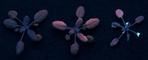
The researchers have a couple of images illustrating their work,
The buildup of fluorescent quantum dots in the leaves of Arabidopsis plants is apparent in this photograph of the plants under ultraviolet light. Credit: Y. Koo/Rice University
This paper is open access but you must be registered on the website.
One final thought about the research, it did take place in a laboratory environment and there doesn’t seem to have been any soil involved so the uptake can not be directly compared (as I understand matters) to the uptake characteristics where plant cultivation requires soil. This seems to have been a study involving hydroponic framing practices.
Researchers, Ingrid Bergin in the Unit for Laboratory Animal Medicine, at the University of Michigan in Ann Arbor and Frank Witzmann in the Department of Cellular and Integrative Physiology, at Indiana University School of Medicine, in Indianapolis, have stated that ingesting food and beverage (translated by me from the more scientific description) with nanoparticles (at today’s current levels) is unlikely to prove toxic. A June 26, 2013 Inderscience news release on EurekAlert describes the researchers’ research and their conclusions,
Writing in a forthcoming issue of the International Journal of Biomedical Nanoscience and Nanotechnology, researchers have compared existing laboratory and experimental animal studies pertaining to the toxicity of nanoparticles most likely to be intentionally or accidentally ingested. Based on their review, the researchers determined ingestion of nanoparticles at likely exposure levels is unlikely to cause health problems, at least with respect to acute toxicity. Furthermore, in vitro laboratory testing, which often shows toxicity at a cellular level, does not correspond well with in vivo testing, which tends to show less adverse effects.
Ingrid Bergin in the Unit for Laboratory Animal Medicine, at the University of Michigan in Ann Arbor and Frank Witzmann in the Department of Cellular and Integrative Physiology, at Indiana University School of Medicine, in Indianapolis, explain that the use of particles that are in the nano size range (from 1 billionth to 100 billionths of a meter in diameter, 1-100 nm, other thereabouts) are finding applications in consumer products and medicine. These include particles such as nano-silver, which is increasingly used in consumer products and dietary supplements for its purported antimicrobial properties. Nanoparticles can have some intriguing and useful properties because they do not necessarily behave in the same chemical and physical ways as non-nanoparticle versions of the same material.
Nanoparticles are now used as natural flavor enhancers in the form of liposomes and related materials, food pigments and in some so-called “health supplements”. They are also used in antibacterial toothbrushes coated with silver nanoparticles, for instance in food and drink containers and in hygienic infant feeding equipment. They are also used to carry pharmaceuticals to specific disease sites in the body to reduce side effects. Nanoparticles actually encompass a very wide range of materials from pure metals and alloys, to metal oxide nanoparticles, and carbon-based and plastic nanoparticles. Because of their increasing utilization in consumer products, there has been concern over whether these small scale materials could have unique toxicity effects when compared to more traditional versions of the same materials.
Difficulties in assessing the health risks of nanoparticles include the fact that particles of differing materials and shapes can have different properties. Furthermore, the route of exposure (e.g. ingestion vs. inhalation) affects the likelihood of toxicity. The U.S. researchers evaluated the current literature specifically with respect to toxicity of ingested nanoparticles. They point out that, in addition to intentional ingestion as with dietary supplements, unintentional ingestion can occur due to nanoparticle presence in water or as a breakdown product from coated consumer goods. Inhaled nanoparticles also represent an ingestion hazard since they are coughed up, swallowed, and eliminated through the intestinal tract.
Based on their review, the team concludes that, “Ingested nanoparticles appear unlikely to have acute or severe toxic effects at typical levels of exposure.” Nevertheless, they add that the current literature is inadequate to assess whether nanoparticles can accumulate in tissues and have long-term effects or whether they might cause subtle alterations in gut microbial populations. The researchers stress that better methods are needed for correlating particle concentrations used for cell-based assessment of toxicity with the actual likely exposure levels to body cells. Such methods may lead to better predictive value for laboratory in vitro testing, which currently over-predicts toxicity of ingested nanoparticles as compared to in vivo testing.
The researchers focused specifically on ingestion via the gastrointestinal tract which I take to mean that they focused largely on nanoparticles in food (eaten) and liquid (swallowed).
I think the abstract further helps to understand the research focus,
The increasing interest in nanoparticles for advanced technologies, consumer products, and biomedical applications has led to great excitement about potential benefits but also concern over the potential for adverse human health effects. The gastrointestinal tract represents a likely route of entry for many nanomaterials, both directly through intentional ingestion or indirectly via nanoparticle dissolution from food containers or by secondary ingestion of inhaled particles. Additionally, increased utilisation of nanoparticles may lead to increased environmental contamination and unintentional ingestion via water, food animals, or fish. The gastrointestinal tract is a site of complex, symbiotic interactions between host cells and the resident microbiome. Accordingly, evaluation of nanoparticles must take into consideration not only absorption and extraintestinal organ accumulation but also the potential for altered gut microbes and the effects of this perturbation on the host. The existing literature was evaluated for evidence of toxicity based on these considerations. Focus was placed on three categories of nanomaterials: nanometals and metal oxides, carbon-based nanoparticles, and polymer/dendrimers with emphasis on those particles of greatest relevance to gastrointestinal exposures.
3M is promising more color on your liquid crystal display (LCD) as a consequence of its new deal with Nanosys Inc. From the June 5, 2012 news item on Nanowerk,
Nanosys Inc. and the Optical Systems Division of 3M Company are joining technologies to provide wide color gamut technology for consumer electronic displays, allowing Liquid Crystal Displays (“LCDs”) to display 50 percent more color.
3M and Nanosys will work together to commercialize Nanosys’ Quantum Dot Enhancement Film(TM) (“QDEF”) technology. QDEF is a drop-in film that LCD manufacturers can integrate with existing production processes. It utilizes the light emitting properties of quantum dots to create an ideal backlight for LCDs — one of the most critical factors in the color and efficiency performance of LCDs.
“Combining the world class-technology and materials expertise of Nanosys with the engineering, design and supply chain capabilities of 3M will unlock a powerful new color viewing experience for consumers,” said Jim Bauman, Vice President of the Optical Systems Division at 3M.
Over the years, 3M technologies have enabled better LCD performance. However, color performance of LCD’s has gone largely unchanged. Current LCDs are limited to displaying 35 percent or less of the visible color spectrum. This means the viewing experience on an LCD is vastly different than what a person sees in the real world. Wide color gamut displays will allow consumers to enjoy more visceral, more immersive and truer to life color.
I was going to post this a few days ago but, luckily, I held back. Dexter Johnson in his June 7, 2012 posting on the Nanoclast blog on the IEEE (Institute of Electrical and Electronics Engineers) website offers an interesting perspective on this deal based on his 2010 interview with Nanosys Inc.’s then Vice President of World Wide Sales and Marketing, Victor Hsia who explained,
Current LED backlights use conventional white LEDs (which are BLUE LEDs with YAG phosphor) that cannot produce saturated GREEN or RED colors. In contrast Nanosys’ Quantum Rail produces a pure white light by using a BLUE LED with Green and Red Quantum Dot phosphors, which results in a tuned white light source that enables over 100 percent NTSC color gamut using the same high volume LCD display manufacturing flow that exists today.”
I’m finding the percentages a little confusing. In 2010, Nanosys could offer over 100% more color for conventional LCD displays. In 2012 and presumably in 2010, the consumer viewing experience offers 35% or less of the color spectrum.
The deal with 3M assures consumers 50% more color than the current 35% we can see. Doesn’t that mean we’d get 52% of the color spectrum with this 3M/Nanosys deal? Please let me know if I got the numbers wrong or made some mistaken assumptions. In the meantime, I suggest taking a look at Dexter’s post for more technical information about the Nanosys technology and more background about LCDs.
I have two items on quantum dots today. The first concerns a toxicity study performed on primates at the University of Buffalo (NY, USA). From the May 22, 2012 news item by Will Soutter for Azonano,
A multi-institute toxicity study on quantum dots in primates has discovered that these nanocrystals are safe for a period of one year.
This finding is encouraging for researchers and physicians looking for novel techniques to treat diseases such as cancer using nanomedicine. The organizations involved in the study included the University at Buffalo, Nanyang Technological University, ChangChun University of Science and Technology, and the Chinese PLA General Hospital.
On digging a little further, I found this information on the University of Buffalo website, from their May 21, 2012 news release,
— Tiny luminescent crystals called quantum dots hold great promise as tools for treating and detecting diseases like cancer.
— A pioneering study to gauge the toxicity of quantum dots in primates has found cadmium-selenide quantum dots to be safe over intervals of time ranging from three months to a year. The study is likely the first to test the safety of quantum dots in primates.
— The authors say more research is needed to determine quantum dots’ long-term effect on health; elevated levels of cadmium from the quantum dots were found in the primates even after 90 days.
The research, which appeared on May 20 in Nature Nanotechnology online , is likely the first to test the safety of quantum dots in primates.
In the study, scientists found that four rhesus monkeys injected with cadmium-selenide quantum dots remained in normal health over 90 days. Blood and biochemical markers stayed in typical ranges, and major organs developed no abnormalities. The animals didn’t lose weight.
Two monkeys observed for an additional year also showed no signs of illness.
The first results are hopeful but there are some concerns,
The new toxicity study — completed by the University at Buffalo, the Chinese PLA General Hospital, China’s ChangChun University of Science and Technology, and Singapore’s Nanyang Technological University — begins to address the concern of health professionals who worry that quantum dots may be dangerous to humans.
The authors caution, however, that more research is needed to determine the nanocrystals’ long-term effects in primates; most of the potentially toxic cadmium from the quantum dots stayed in the liver, spleen and kidneys of the animals studied over the 90-day period.
…
The cadmium build-up, in particular, is a serious concern that warrants further investigation, said Ken-Tye Yong, a Nanyang Technological University assistant professor who began working with Prasad [Paras N. Prasad] on the study as a postdoctoral researcher at UB.
Unusually, this article seems to be open access at Nature Nanotechnology,
Ling Ye, Ken-Tye Yong, Liwei Liu, Indrajit Roy, Rui Hu, Jing Zhu, Hongxing Cai, Wing-Cheung Law, Jianwei Liu, Kai Wang, Jing Liu, Yaqian Liu, Yazhuo Hu, Xihe Zhang, Mark T. Swihart, and Paras N. Prasad
The acquisition of an Israeli quantum dot company by Merck is my second bit of quantum dot news, from the May 22, 2012 news item on Nanowerk,
Merck announced today that within the scope of a capital increase by the Israeli start-up company QLight Nanotech, it is acquiring an interest in the Jerusalem-based company. QLight Nanotech is a spin-off subsidiary of Yissum, the technology transfer company of the Hebrew University of Jerusalem. QLight Nanotech develops products for use in displays and energy-efficient light sources based on semiconductor nanoparticles known as quantum dots.
I understood that Merck was a pharmaceutical company so I was bit surprised to see this (from the May 22, 2012 news item on the Solid State Technology website)
“I am excited that our basic science discoveries on semiconductor nanocrystals are now being realized in innovative technological applications. The partnership with Merck, a world leader in materials for display applications, is a synergistic one allowing us at Qlight Nanotech to implement advanced chemicals manufacturing and applications’ know-how,” said the scientific founder of QLight Nanotech, Professor Uri Banin of the Hebrew University of Jerusalem, who will continue to support the company as a shareholder and advisor alongside of Yissum.
In fact, Merck bills itself as a pharmaceuticals and a s chemicals company.
I’ve done very little writing about quantum dots (so much nano, so little time) but there’s been a fair amount of activity lately which has piqued my interest. In the last few days researchers at Kansas State University have been getting noticed for being able to control the size and shape of the graphene quantum dots they produce. This one has gotten extensive coverage online including this May 17, 2012 news item on physorg.com,
Vikas Berry, William H. Honstead professor of chemical engineering, has developed a novel process that uses a diamond knife to cleave graphite into graphite nanoblocks, which are precursors for graphene quantum dots. These nanoblocks are then exfoliated to produce ultrasmall sheets of carbon atoms of controlled shape and size.
By controlling the size and shape, the researchers can control graphene’s properties over a wide range for varied applications, such as solar cells, electronics, optical dyes, biomarkers, composites and particulate systems. Their work has been published in Nature Communications and supports the university’s vision to become a top 50 public research university by 2025. The article is available online.
Here’s an image of graphene being cut by a diamond knife from the May 16, 2012 posting by jtorline on the K-State News blog,
Molecular dynamics snapshot of stretched graphene being nanotomed via a diamond knife.
Here’s why standardizing the size is so important,
While other researchers have been able to make quantum dots, Berry’s research team can make quantum dots with a controlled structure in large quantities, which may allow these optically active quantum dots to be used in solar cell and other optoelectronic applications. [emphasis mine]
While all this is happening in Kansas, the Econ0mist magazine published a May 12, 2012 article about some important quantum dot optoelectronic developments in Spain (an excellent description for relative beginners is given and, if this area interests you, I’d suggest reading it in full),
Actually converting the wonders of graphene into products has been tough. But Frank Koppens and his colleagues at the Institute of Photonic Sciences in Barcelona think they have found a way to do so. As they describe in Nature Nanotechnology, they believe graphene can be used to make ultra-sensitive, low-cost photodetectors.
…
A typical photodetector is made of a silicon chip a few millimetres across onto which light is focused by a small lens. Light striking the chip knocks electrons free from some of the silicon atoms, producing a signal that the chip’s electronics convert into a picture or other useful information. …
Silicon photodetectors suffer, though, from a handicap: they are inflexible. Nor are they particularly cheap. And they are not that sensitive. They absorb only 10-20% of the light that falls on to them. For years, therefore, engineers have been on the lookout for a cheap, bendable, sensitive photodetector. …
By itself, graphene is worse than silicon at absorbing light. According to Dr Koppens only 2.7% of the photons falling on it are captured. But he and his colleague Gerasimos Konstantatos have managed to increase this to more than 50% by spraying tiny crystals of lead sulphide onto the surface of the material.
So combining the ability to size quantum dots uniformly with this discovery on how to make graphene more sensitive (and more useful in potential products) with quantum dots suggests some very exciting possibilities including this one mentioned by Dexter Johnson (who’s living in Spain these days) in his May 16, 2012 posting on Nanoclast (on the Institute of Electrical and Electronics Engineers [IEEE] website),
The researchers offer a range of applications for the graphene-and-quantum-dot combination, including digital cameras and sensors. [emphasis mine] But it seems the researchers seem particularly excited about one application in particular. They expect the material will be used for night-vision technologies in automobiles—an application I have never heard trotted out before in relation to nanotech.
You can get more insights, more precise descriptions if you want to follow up from the Econ0mist article, and Dexter’s links to more information about the research in his posting.
In my final roundup piece, I received a news release (dated April 24, 2012) about a quantum dot commercialization project at the University of Utah,
One of the biggest challenges for advancing quantum dots is the manufacturing process. Conventional processes are expensive, require high temperatures and produce low yields. However, researchers at the University of Utah believe they have a solution. They recently formed a startup company called Navillum Nanotechnologies, and their efforts are gaining national attention with help from a team of M.B.A. students from the David Eccles School of Business.
The students recently won first place and $100,000 at the regional CU Cleantech New Venture Challenge. The student competition concluded at the University of Colorado in Boulder on Friday, April 20. The student team advances to the national championship, which will be held in June in Washington, D.C. Student teams from six regions will compete for additional prizes and recognition at the prestigious event. Other regional competitions were held at MIT, Cal Tech, the University of Maryland, Clean Energy Trust (Chicago) and Rice University. All the competitions are financed by the U.S. Department of Energy.
The students will be competing in the national Clean Energy Business Plan Competition taking place June 12-13, 2012 in Washington, D.C. Here are a few more details from the national competition webpage,
Winners of the six regional competitions will represent their home universities and regions as they vie for the honor of presenting the best clean energy business plan before a distinguished panel of expert judges and invited guests from federal agencies, industry, national labs and the venture capital community.
Confirmed Attendees include:
The Honorable Steven Chu Energy Secretary [US federal government]
Dr. David Danielson Assistant Secretary, EERE [US Dept. of Energy, energy efficiency and renewable energy technologies)
Dr. Karina Edmonds Technology Transfer Coordinator [US Dept. of Energy]
Mr. Todd Park Chief Technology Officer, White House
Professors Shana Kelley and Ted Sargent (he was last mentioned in my June 28, 2011 posting on colloidal quantum dots) have published their findings on quantum dots, self-assembly, and luninescence in Nature Nanotechnology. From the July 10, 2011 news item on Nanowerk,
“Nanotechnologists have for many years been captivated by quantum dots – particles of semiconductor that can absorb and emit light efficiently, and at custom-chosen wavelengths,” explained co-author Kelley, a Professor at the Leslie Dan Faculty of Pharmacy, the Department of Biochemistry in the Faculty of Medicine, and the Department of Chemistry in the Faculty of Arts & Science. “What the community has lacked – until now – is a strategy to build higher-order structures, or complexes, out of multiple different types of quantum dots. This discovery fills that gap.”
The team combined its expertise in DNA and in semiconductors to invent a generalized strategy to bind certain classes of nanoparticles to one another.
“The credit for this remarkable result actually goes to DNA: its high degree of specificity – its willingness to bind only to a complementary sequence – enabled us to build rationally-engineered, designer structures out of nanomaterials,” said Sargent, a Professor in The Edward S. Rogers Sr. Department of Electrical & Computer Engineering at the University of Toronto, who is also the Canada Research Chair in Nanotechnology. “The amazing thing is that our antennas built themselves – we coated different classes of nanoparticles with selected sequences of DNA, combined the different families in one beaker, and nature took its course. The result is a beautiful new set of self-assembled materials with exciting properties.”
For anyone who can get past Nature Nanotechnology’s paywall, the article is titled, “DNA-based programming of quantum dot valency, self-assembly and luminescence”, and it was released on July 10, 2011.
A flat layer of carbon atoms packed into a two-dimensional honeycomb arrangement, graphene is being touted as a miracle (it seems) material which will enable new kinds of electronic products. Recently, there have been a number of news items and articles featuring graphene research.
Here’s my roundup of the latest and greatest graphene news. I’m starting with an application that is the closest to commercialization: IBM recently announced the creation of the first graphene-based integrated circuit. From the Bob Yirka article dated June 10, 2011 on physorg.com,
Taking a giant step forward in the creation and production of graphene based integrated circuits, IBM has announced in Science, the fabrication of a graphene based integrated circuit [IC] on a single chip. The demonstration chip, known as a radio frequency “mixer” is capable of producing frequencies up to 10 GHz, and demonstrates that it is possible to overcome the adhesion problems that have stymied researchers efforts in creating graphene based IC’s that can be used in analog applications such as cell phones or more likely military communications.
The graphene circuits were started by growing a two or three layer graphene film on a silicon surface which was then heated to 1400°C. The graphene IC was then fabricated by employing top gated, dual fingered graphene FET’s (field-effect transistors) which were then integrated with inductors. The active channels were made by spin-coating the wafer with a thin polymer and then applying a layer of hydrogen silsequioxane. The channels were then carved by e-beam lithography. Next, the excess graphene was removed with an oxygen plasma laser, and then the whole works was cleaned with acetone. The result is an integrated circuit that is less than 1mm2 in total size.
Meanwhile, there’s a graphene research project in contention for a major research prize in Europe. Worth 1B Euros, the European Union’s 2011 pathfinder programme (Future and Emerging Technologies [Fet11]) in information technology) will select two from six pilot actions currently under way to be awarded a Flagship Initiative prize. From the Fet11 flagships project page,
FET Flagships are large-scale, science-driven and mission oriented initiatives that aim to achieve a visionary technological goal. The scale of ambition is over 10 years of coordinated effort, and a budget of up to one billion Euro for each Flagship. They initiatives are coordinated between national and EU programmes and present global dimensions to foster European leadership and excellence in frontier research.
To prepare the launch of the FET Flagships, 6 Pilot Actions are funded for a 12-month period starting in May 2011. In the second half of 2012 two of the Pilots will be selected and launched as full FET Flagship Initiatives in 2013.
Here’s the description of the Graphene Science and technology for ICT and beyond pilot action,
Graphene, a new substance from the world of atomic and molecular scale manipulation of matter, could be the wonder material of the 21st century. Discovering just how important this material will be for Information and Communication Technologies is the long term focus of the Flagship Initiative, simply called, GRAPHENE. This aims to explore revolutionary potentials, in terms of both conventional as well as radically new fields of Information and Communication Technologies applications.
Bringing together multiple disciplines and addressing research across a whole range of issues, from fundamental understandings of material properties to Graphene production, the Flagship will provide the platform for establishing European scientific and technological leadership in the application of Graphene to Information and Communication Technologies. The proposed research includes coverage of electronics, spintronics, photonics, plasmonics and mechanics, all based on Graphene.
[Project Team:]
Andrea Ferrari, Cambridge University, UK
Jari Kinaret, Chalmers University, Sweden
Vladimir Falko, Lancaster University, UK
Jani Kivioja, NOKIA, Finland [emphases mine]
Not so coincidentally (given one member of the team is associated with Nokia and another is associated with Cambridge University), the Nokia Research Centre jointly with Cambridge University issued a May 4, 2011 news release (I highlighted it in my May 6, 2011 posting [scroll down past the theatre project information]) about the Morph concept (a rigid, flexible, and stretchable phone/blood pressure cuff/calculator/and other electronic devices in one product) which they have been publicizing for years now. The news release concerned itself with how graphene would enable the researchers to take the Morph from idea to actuality. The webpage for the Graphene Pilot Action is here.
There’s something breathtaking when there is no guarantee of success about the willingness to invest up to 1B Euros in a project that spans 10 years. We’ll have to wait until 2013 before learning whether the graphene project will be one of the two selected as Flagship Initiatives.
I must say the timing for the 2010 Nobel Prize for Physics which went to two scientists (Andre Geim and Konstantin Novoselov) for their groundbreaking work with graphene sems interesting (featured in my Oct. 7, 2010 posting) in light of this graphene activity.
The rest of these graphene items are about research that could lay the groundwork for future commercialization.
Hui-Ming Cheng and co-workers from the Chinese Academy of Sciences’ Institute of Metal Research at Shenyang have now devised a chemical vapor deposition (CVD) method for turning graphene sheets into porous three-dimensional ‘foams’ with extremely high conductivity (“Three-dimensional flexible and conductive interconnected graphene networks grown by chemical vapour deposition” [published in Nature Materials 10, 424–428 (2011) doi:10.1038/nmat3001 Published online 10 April 2011]). By permeating this foam with a siloxane-based polymer, the researchers have produced a composite that can be twisted, stretched and bent without harming its electrical or mechanical properties.
Here’s an image from the Nature Publishing Group (NPG) of both the vapour and the bendable, twistable, stretchable composite (downloaded from the news item on Nanowerk where you can find a larger version of the image),
The ‘elastic’ conductor (image to the right) reminds me of the ‘paper’ phone which I wrote about May 8, 2011 and May 12, 2011. (It’s a project where teams from Queen’s University [in Ontario] and Arizona State University are working to create flexible screens that give you telephony, music playing and other capabilities much like the Morph concept.)
Researchers in Singapore have developed a graphene quantum dot using a C60 (a buckminster fullerene). From the June 13, 2011 news item (Graphene: from spheres to perfect dots) on Nanowerk,
An electron trapped in a space of just a few nanometers across behaves very differently to one that is free. Structures that confine electrons in all three dimensions can produce some useful optical and electronic effects. Known as quantum dots, such structures are being widely investigated for use in new types of optical and electronics technologies, but because they are so small it is difficult to fabricate quantum dots reproducibly in terms of shape and size. Researchers from the National University of Singapore (NUS) and A*STAR have now developed a technique that enables graphene quantum dots of a known size to be created repeatedly and quickly (“Transforming C60 molecules into graphene quantum dots” [published in Nature Nanotechnology 6, 247–252 (2011) doi:10.1038/nnano.2011.30 Published online 20 March 2011]).
This final bit is about a nano PacMan that allows for more precise patterning from a June 13, 2011 article written by Michael Berger,
A widely discussed method for the patterning of graphene is the channelling of graphite by metal nanoparticles in oxidizing or reducing environments (see for instance: “Nanotechnology PacMan cuts straight graphene edges”).
“All previous studies of channelling behavior have been limited by the need to perform the experiment ex situ, i.e. comparing single ‘before’ and ‘after’ images,” Peter Bøggild, an associate professor at DTU [Danish Technical University] Nanotech, explains to Nanowerk. “In these and other ex situ experiments the dynamic behavior must be inferred from the length of channels and heating time after completion of the experiment, with the rate of formation of the channel assumed to be consistent over the course of the experiment.”
In new work, reported in the June 9, 2011 advance online edition of Nano Letters (“Discrete dynamics of nanoparticle channelling in suspended graphene” [published in Nano Letters, Article ASAP, DOI: 10.1021/nl200928k, Publication Date (Web): June 9, 2011]), Bøggild and his team report the nanoscale observation of this channelling process by silver nanoparticles in an oxygen atmosphere in-situ on suspended mono- and bilayer graphene in an environmental transmission electron microscope, enabling direct concurrent observation of the process, impossible in ex-situ experiments.
Personally, I love the youtube video I’ve included here largely because it features blobs (as many of these videos do) where they’ve added music and titles (many of these videos do not) so you can better appreciate the excitement,
From the article by Michael Berger,
As a result of watching this process occur live in a transmission electron microscope, the researchers say they have seen many details that were hidden before, and video really brings the “nano pacman” behavior to life …
There’s a reason why they’re so interested in cutting graphene,
“With a deeper understanding of the fine details we hope to one day use this nanoscale channelling behavior to directly cut desired patterns out of suspended graphene sheets, with a resolution and accuracy that isn’t achievable with any other technique,” says Bøggild. “A critical advantage here is that the graphene crystal structure guides the patterning, and in our case all of the cut edges of the graphene are ‘zigzag’ edges.”
So there you have it. IBM creates the first integrated graphene-based circuit, there’s the prospect of a huge cash prize for a 10-year project on graphene so they could produce the long awaited Morph concept and other graphene-based electronics products while a number of research teams around the world continue teasing out its secrets with graphene ‘foam’ projects, graphene quantum dots, and nano PacMen who cut graphene’s zigzag edges with precision.
ETA June 16, 2011: For those interested in the business end of things, i.e. market value of graphene-based products, Cameron Chai features a report, Graphene: Technologies, Applications, and Markets, in his June 16, 2011 news item on Azonano.