Tag Archives: University of Illinois at Urbana-Champaign

Shrinky Dinks* instrumental for new nanowires technique

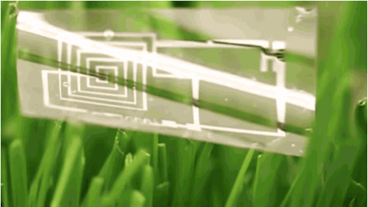
Shrinky Dinks, a material used for children’s arts and crafts projects, has proved instrumental for developing a new technique to close the gap between nanowires. From a July 1, 2014 news item on Nanowerk (Note: A link has been removed),

How do you put a puzzle together when the pieces are too tiny to pick up? Shrink the distance between them.

Engineers at the University of Illinois at Urbana-Champaign are using Shrinky Dinks, plastic that shrinks under high heat, to close the gap between nanowires in an array to make them useful for high-performance electronics applications. The group published its technique in the journal Nano Letters (“Assembly and Densification of Nanowire Arrays via Shrinkage”).

A July 1, 2014 University of Illinois at Urbana-Champaign news release, which originated the news item, provides more details about the new technique,

Nanowires are extremely fast, efficient semiconductors, but to be useful for electronics applications, they need to be packed together in dense arrays. Researchers have struggled to find a way to put large numbers of nanowires together so that they are aligned in the same direction and only one layer thick.

“Chemists have already done a brilliant job in making nanowires exhibit very high performance. We just don’t have a way to put them into a material that we can handle,” said study leader SungWoo Nam, a professor of mechanical science and engineering at the U. of I. “With the shrinking approach, people can make nanowires and nanotubes using any method they like and use the shrinking action to compact them into a higher density.”

The researchers place the nanowires on the Shrinky Dinks plastic as they would for any other substrate, but then shrink it to bring the wires much closer together. This allows them to create very dense arrays of nanowires in a simple, flexible and very controllable way.

The shrinking method has the added bonus of bringing the nanowires into alignment as they increase in density. Nam’s group demonstrated how even wires more than 30 degrees off-kilter can be brought into perfect alignment with their neighbors after shrinking.

“There’s assembly happening at the same time as the density increases,” Nam said, “so even if the wires are assembled in a disoriented direction we can still use this approach.”

The plastic is clamped before baking so that it only shrinks in one direction, so that the wires pack together but do not buckle. Clamping in different places could direct the arrays into interesting formations, according to Nam. The researchers also can control how densely the wires pack by varying the length of time the plastic is heated. They also are exploring using lasers to precisely shrink the plastic in specific patterns.

Nam first had the idea for using Shrinky Dinks plastic to assemble nanomaterials after seeing a microfluidics device that used channels made of shrinking plastic. He realized that the high degree of shrinking and the low cost of plastic could have a huge impact on nanowire assembly and processing for applications.

“I’m interested in this concept of synthesizing new materials that are assembled from nanoscale building blocks,” Nam said. “You can create new functions. For example, experiments have shown that film made of packed nanowires has properties that differ quite a bit from a crystal thin film.”

One application the group is now exploring is a thin film solar cell, made of densely packed nanowires, that could harvest energy from light much more efficiently than traditional thin-film solar cells.

I have featured the Shrinky Dinks product and its use for nanoscale fabrication before in an Aug. 16, 2010 posting which featured this reply from the lead researcher for that project on nanopatterning,

ETA Aug.17.10: I also contacted Teri W. Odom, professor at Northwestern University about why they use Slinky Dinks in their work. She very kindly responded with this:

Part of what we are interested in is the development of low-cost nanofabrication tools that can create macroscale areas of nanoscale patterns in a single step. For a variety of reasons, this end-product is hard to obtain—even though we and others have chipped away at this problem for years.

As an example, to achieve smaller and smaller separations between patterns, either expensive, top-down serial tools (such as electron beam lithography or scanning probe techniques) or bottom-up assembly methods need to be used. However, the former cannot easily create large areas of patterns, and the latter cannot readily control the separations of patterns.

We needed a way to obtain nanopatterns separated by specific distances on-demand. Here is where the Shrinky Dinks material comes in. My student had read a paper (published in 2007 in Lab on a Chip) about how this material was used to make microscale patterns starting from a pattern printed using a laser printer. I imagine his thought was: if this material could be used for microscale patterns, why not for nanoscale ones? It would be cheap, and it’s easy to order.

So, we combined this substrate with our new molding method—solvent assisted nanoscale embossing (SANE)—and could now heat the material to shrink the spacing between patterns. And thus, in some sense, we made available to any lab some of the capabilities of the billion-dollar nanofabrication industry for less than one-hundred dollars.

Getting back to this latest use of Shrinky Dinks, here’s a link to and a citation for the ‘nanowires’ research paper,

Assembly and Densification of Nanowire Arrays via Shrinkage by Jaehoon Bang, Jonghyun Choi, Fan Xia, Sun Sang Kwon, Ali Ashraf, Won Il Park, and SungWoo Nam. Nano Lett., 2014, 14 (6), pp 3304–3308 DOI: 10.1021/nl500709p Publication Date (Web): May 16, 2014
Copyright © 2014 American Chemical Society

This paper is behind a paywall.

* ‘dinks’ in headline changed to ‘Dinks’ on July 2, 2014 at 1150 hours PDT.

Dimpling can be more than cute, morphable surfaces (smorphs) from MIT (Massachusetts Institute of Technology)

A morphable surface developed by an MIT team can change surface texture — from smooth to dimply, and back again — through changes in pressure. When the inside pressure is reduced, the flexible material shrinks, and the stiffer outer layer wrinkles. Increasing pressure returns the surface to a smooth state.

A June 24, 2014 news item on Nanowerk features a story about the origins of the dimpled golf ball, aerodynamics, and some very pink material (Note: A link has been removed),

There is a story about how the modern golf ball, with its dimpled surface, came to be: In the mid-1800s, it is said, new golf balls were smooth, but became dimpled over time as impacts left permanent dents. Smooth new balls were typically used for tournament play, but in one match, a player ran short, had to use an old, dented one, and realized that he could drive this dimpled ball much further than a smooth one.

Whether that story is true or not, testing over the years has proved that a golf ball’s irregular surface really does dramatically increase the distance it travels, because it can cut the drag caused by air resistance in half. Now researchers at MIT are aiming to harness that same effect to reduce drag on a variety of surfaces — including domes that sometimes crumple in high winds, or perhaps even vehicles.

Detailed studies of aerodynamics have shown that while a ball with a dimpled surface has half the drag of a smooth one at lower speeds, at higher speeds that advantage reverses. So the ideal would be a surface whose smoothness can be altered, literally, on the fly — and that’s what the MIT team has developed.

The new work is described in a paper in the journal Advanced Materials (“Smart Morphable Surfaces for Aerodynamic Drag Control”) by MIT’s Pedro Reis and former MIT postdocs Denis Terwagne (now at the Université Libre de Bruxelles in Belgium) and Miha Brojan (now at the University of Ljubljana in Slovenia).

esearchers made this sphere to test their concept of morphable surfaces. Made of soft polymer with a hollow center, and a thin coating of a stiffer polymer, the sphere becomes dimpled when the air is pumped out of the hollow center, causing it to shrink. (Photo courtesy of the MIT researchers)

Researchers made this sphere to test their concept of morphable surfaces. Made of soft polymer with a hollow center, and a thin coating of a stiffer polymer, the sphere becomes dimpled when the air is pumped out of the hollow center, causing it to shrink. (Photo courtesy of the MIT researchers)

A June 24, 2014 MIT (Massachusetts Institute of Technology) news release (also on EurekAlert) by David Chandler, which originated the news item, provides more detail about the work,

The ability to change the surface in real time comes from the use of a multilayer material with a stiff skin and a soft interior — the same basic configuration that causes smooth plums to dry into wrinkly prunes. To mimic that process, Reis and his team made a hollow ball of soft material with a stiff skin — with both layers made of rubberlike materials — then extracted air from the hollow interior to make the ball shrink and its surface wrinkle.

“Numerous studies of wrinkling have been done on flat surfaces,” says Reis, an assistant professor of mechanical engineering and civil and environmental engineering. “Less is known about what happens when you curve the surface. How does that affect the whole wrinkling process?”

The answer, it turns out, is that at a certain degree of shrinkage, the surface can produce a dimpled pattern that’s very similar to that of a golf ball — and with the same aerodynamic properties.

The aerodynamic properties of dimpled balls can be a bit counterintuitive: One might expect that a ball with a smooth surface would sail through the air more easily than one with an irregular surface. The reason for the opposite result has to do with the nature of a small layer of the air next to the surface of the ball. The irregular surface, it turns out, holds the airflow close to the ball’s surface longer, delaying the separation of this boundary layer. This reduces the size of the wake — the zone of turbulence behind the ball — which is the primary cause of drag for blunt objects.

When the researchers saw the wrinkled outcomes of their initial tests with their multilayer spheres, “We realized that these samples look just like golf balls,” Reis says. “We systematically tested them in a wind tunnel, and we saw a reduction in drag very similar to that of golf balls.”

Because the surface texture can be controlled by adjusting the balls’ interior pressure, the degree of drag reduction can be controlled at will. “We can generate that surface topography, or erase it,” Reis says. “That reversibility is why this is pretty interesting; you can switch the drag-reducing effect on and off, and tune it.”

As a result of that variability, the team refers to these as “smart morphable surfaces” — or “smorphs,” for short. The pun is intentional, Reis says: The paper’s lead author — Terwagne, a Belgian comics fan — pointed out that one characteristic of Smurfs cartoon characters is that no matter how old they get, they never develop wrinkles.

Terwagne says that making the morphable surfaces for lab testing required a great deal of trial-and-error — work that ultimately yielded a simple and efficient fabrication process. “This beautiful simplicity to achieve a complex functionality is often used by nature,” he says, “and really inspired me to investigate further.”

Many researchers have studied various kinds of wrinkled surfaces, with possible applications in areas such as adhesion, or even unusual optical properties. “But we are the first to use wrinkling for aerodynamic properties,” Reis says.

The drag reduction of a textured surface has already expanded beyond golf balls: The soccer ball being used at this year’s World Cup, for example, uses a similar effect; so do some track suits worn by competitive runners. For many purposes, such as in golf and soccer, constant dimpling is adequate, Reis says.

But in other uses, the ability to alter a surface could prove useful: For example, many radar antennas are housed in spherical domes, which can collapse catastrophically in very high winds. A dome that could alter its surface to reduce drag when strong winds are expected might avert such failures, Reis suggests. Another application could be the exterior of automobiles, where the ability to adjust the texture of panels to minimize drag at different speeds could increase fuel efficiency, he says.

Delightful is not the first adjective that jumps to my mind when describing this work but I’m not an engineer (from the news release),

John Rogers, a professor of materials research and engineering at the University of Illinois at Urbana-Champaign who was not involved in this work, says, “It represents a delightful example of how controlled processes of mechanical buckling can be used to create three-dimensional structures with interesting aerodynamic properties. The type of dynamic tuning of sophisticated surface morphologies made possible by this approach would be difficult or impossible to achieve in any other way.”

Here’s a link to and a citation for the paper,

Smart Morphable Surfaces for Aerodynamic Drag Control by Denis Terwagne, Miha Brojan, and Pedro M. Reis. Advanced Materials DOI: 10.1002/adma.201401403 Article first published online: 23 JUN 2014

© 2014 WILEY-VCH Verlag GmbH & Co. KGaA, Weinheim

This paper is behind a paywall.

E-tattoo without the nanotech

John Rogers and his team at the University of Illinois and a colleague’s (Yonggang Huang) team at Northwestern University have devised an ‘electronic tattoo’ (a soft, stick-on patch) made up from materials that anyone can purchase off-the-shelf. Rogers is known for his work with nanomaterials (my Aug. 10, 2012 posting titled ‘Surgery with fingertip control‘ mentioned a silicon nanomembrane that can be fitted onto the fingertips for possible use in surgical procedures) and with electronics (my Aug. 12, 2011 posting titled: ‘Electronic tattoos‘ mentioned his earlier attempts at developing e-tattoos).

This latest effort from Rogers and his multi-university team is mentioned in an April 4, 2014 article by Mark Wilson for Fast Company,

About a year ago, University of Illinois researcher John Rogers revealed a pretty amazing creation: a circuit that, rather than living on an inflexible board, could stick to and move with someone’s skin just like an ink stamp. But like any early research, it was mostly a proof-of-concept, and it would require relatively expensive, custom-printed electronics to work.

Today, Rogers, in conjunction with Northwestern University’s Yonggang Huang, has published details on version 2.0 in Science, revealing that this once-esoteric project has more immediate, mass market appeal.

… It means that you could create a wearable electronic that’s one-part special sticky circuit board, every other part whatever-the-hell-you-manufactured-in-China. This flexible circuit could accommodate a stock battery, an accelerometer, a Wi-Fi chip, and a Bluetooth circuitry, for instance, all living on your skin rather than inside your iPhone. And as an added bonus, it would be relatively cheap.

A University of Illinois April ?, 2014 news release describes Rogers, his multi-university team, and their current (pun intended) e-tattoo,

Engineers at the University of Illinois at Urbana-Champaign and Northwestern University have demonstrated thin, soft stick-on patches that stretch and move with the skin and incorporate commercial, off-the-shelf chip-based electronics for sophisticated wireless health monitoring.

The patches stick to the skin like a temporary tattoo and incorporate a unique microfluidic construction with wires folded like origami to allow the patch to bend and flex without being constrained by the rigid electronics components. The patches could be used for everyday health tracking – wirelessly sending updates to your cellphone or computer – and could revolutionize clinical monitoring such as EKG and EEG testing – no bulky wires, pads or tape needed.

“We designed this device to monitor human health 24/7, but without interfering with a person’s daily activity,” said Yonggang Huang, the Northwestern University professor who co-led the work with Illinois professor John A. Rogers. “It is as soft as human skin and can move with your body, but at the same time it has many different monitoring functions. What is very important about this device is it is wirelessly powered and can send high-quality data about the human body to a computer, in real time.”

The researchers did a side-by-side comparison with traditional EKG and EEG monitors and found the wireless patch performed equally to conventional sensors, while being significantly more comfortable for patients. Such a distinction is crucial for long-term monitoring, situations such as stress tests or sleep studies when the outcome depends on the patient’s ability to move and behave naturally, or for patients with fragile skin such as premature newborns.

Rogers’ group at Illinois previously demonstrated skin electronics made of very tiny, ultrathin, specially designed and printed components. While those also offer high-performance monitoring, the ability to incorporate readily available chip-based components provides many important, complementary capabilities in engineering design, at very low cost.

“Our original epidermal devices exploited specialized device geometries – super thin, structured in certain ways,” Rogers said. “But chip-scale devices, batteries, capacitors and other components must be re-formulated for these platforms. There’s a lot of value in complementing this specialized strategy with our new concepts in microfluidics and origami interconnects to enable compatibility with commercial off-the-shelf parts for accelerated development, reduced costs and expanded options in device types.”

The multi-university team turned to soft microfluidic designs to address the challenge of integrating relatively big, bulky chips with the soft, elastic base of the patch. The patch is constructed of a thin elastic envelope filled with fluid. The chip components are suspended on tiny raised support points, bonding them to the underlying patch but allowing the patch to stretch and move.

One of the biggest engineering feats of the patch is the design of the tiny, squiggly wires connecting the electronics components – radios, power inductors, sensors and more. The serpentine-shaped wires are folded like origami, so that no matter which way the patch bends, twists or stretches, the wires can unfold in any direction to accommodate the motion. Since the wires stretch, the chips don’t have to.

Skin-mounted devices could give those interested in fitness tracking a more complete and accurate picture of their activity level.

“When you measure motion on a wristwatch type device, your body is not very accurately or reliably coupled to the device,” said Rogers, a Swanlund Professor of Materials Science and Engineering at the U. of I. “Relative motion causes a lot of background noise. If you have these skin-mounted devices and an ability to locate them on multiple parts of the body, you can get a much deeper and richer set of information than would be possible with devices that are not well coupled with the skin. And that’s just the beginning of the rich range of accurate measurements relevant to physiological health that are possible when you are softly and intimately integrated onto the skin.”

The researchers hope that their sophisticated, integrated sensing systems could not only monitor health but also could help identify problems before the patient may be aware. For example, according to Rogers, data analysis could detect motions associated with Parkinson’s disease at its onset.

“The application of stretchable electronics to medicine has a lot of potential,” Huang said. “If we can continuously monitor our health with a comfortable, small device that attaches to our skin, it could be possible to catch health conditions before experiencing pain, discomfort and illness.”

Here’s a link to and a citation for the paper,

Soft Microfluidic Assemblies of Sensors, Circuits, and Radios for the Skin by Sheng Xu, Yihui Zhang, Lin Jia, Kyle E. Mathewson, Kyung-In Jang, Jeonghyun Kim, Haoran Fu, Xian Huang, Pranav Chava, Renhan Wang, Sanat Bhole, Lizhe Wang, Yoon Joo Na, Yue Guan, Matthew Flavin, Zheshen Han, Yonggang Huang, & John A. Rogers. Science 4 April 2014: Vol. 344 no. 6179 pp. 70-74 DOI: 10.1126/science.1250169

This paper is behind a paywall.

Institute for Genomic Biology’s Art of Science 3.0

I like pretty pictures,


Progenitor cells fusing and differentiating into contractile skeletal muscle tissue (Tissue engineering is a promising strategy that could one day provide a cure for patients that need replacements for damaged tissues and organs. Here, the researchers show how stem cells can mature to form skeletal muscle in a matrix bed of proteins. The differentiated muscle fibers are contractile within two weeks) Multiphoton Confocal Microscope Zeiss 710 with Mai Tai eHP Ti: sapphire laser Vincent Chan Rashid Bashir Lab, Laboratory of Integrated Biomedical Micro/Nanotechnology & Applications http://libna.mntl.illinois.edu/

Progenitor cells fusing and differentiating into contractile skeletal muscle tissue (Tissue engineering is a promising strategy that could one day provide a cure for patients that need replacements for damaged tissues and organs. Here, the researchers show how stem cells can mature to form skeletal muscle in a matrix bed of proteins. The differentiated muscle fibers are contractile within two weeks)
Multiphoton Confocal Microscope Zeiss 710 with Mai Tai eHP Ti: sapphire laser
Vincent Chan
Rashid Bashir Lab, Laboratory of Integrated Biomedical
Micro/Nanotechnology & Applications
http://libna.mntl.illinois.edu/

The image I’ve selected is part of the Art of Science 3.0 exhibit being displayed at Chicago’s Midway airport, as per a Jan. 21, 2014 news item on Nanowerk,

An art exhibit at Chicago’s Midway Airport features images created by using microscopy equipment by ZEISS. Researchers from the Institute for Genomic Biology (IGB) Core Facilities, affiliated with the University of Illinois at Urbana-Champaign, used state-of-the-art microscopes for pioneering research to capture images that address significant problems facing humanity related to health, agriculture, energy and the environment. Twelve different images from IGB’s innovative research have been turned into pieces of artwork that travelers can view while using the airport. Five of the images in the exhibit were produced using ZEISS equipment.

You can find all 12 images on the Art of Science 3.0 Facebook page here.

As for whether or not you will see this exhibit if you should be at the Midway Airport, that’s a little difficult to determine. It was an Oct. 25, 2013 Zeiss press release which originated the Jan. 2014 news item on Nanowerk and I can’t find any information in the press release or elsewhere about the airport exhibition dates.

There is a bit more information about the Art of Science 3.0 exhibit (both at the airport. online, and elsewhere) in this undated Institute for Genomic Biology  (IGB) news release,

The exhibit, located past security in Concourse A, features images used in the Institute’s innovative research projects that address significant problems facing humanity related to health, agriculture, energy and the environment.

“Art is a really cool way to learn and jumpstart conversations about research,” said Kathryn Faith Coulter, the Institute’s multimedia design specialist and exhibit’s managing artist. “By sparking a natural curiosity through these vibrant images, we hope people will discover how the research conducted at the University of Illinois relates to their families, friends, and communities.”

The exhibit, which includes two 10-foot banners and 10 pictures, illustrates the microscopic subjects that researchers are able to capture through the Institute’s Core Facilities, which provides faculty and students from across the Urbana campus and east-central region resources for biological microscopy and image analysis.

“This exhibit includes images from a variety of scientific disciplines, from coral polyps to kidney stones and human colon cancer cells,” said Glenn Fried, Director of Core Facilities. “These images represent much more than art. They represent scientific breakthroughs and discoveries that will impact how we treat human diseases, produce abundant food, and fuel a technologically-driven society.”

By the way, there will be an Art of Science exhibit 4.0 later this year (2014), according to the IGB news release,

The Art of Science 4.0 exhibit will be held April 3–7, 2014 at the indi go Artist Co-Op gallery, with an opening reception on April 3.

You can find out more about the  Institute for Genomic Biology here..

Similarities between biological molecules and synthetic nanocrystals extend beyond size

Researchers at the University of Illinois at Urbana-Champaign have determined that there are more similarities between biological molecules and synthetic nanocrystals than formerly believed, according to a Dec. 17, 2013 news item on Nanowerk (Note: A link has been removed),

Researchers have long thought that biological molecules and synthetic nanocrystals were similar only in size. Now, University of Illinois at Urbana-Champaign chemists have found that they can add reactivity to the list of shared traits. Atoms in a nanocrystal can cooperate with each other to facilitate binding or switching, a phenomenon widely found in biological molecules.

The finding could catalyze manufacturing of nanocrystals for smart sensors, solar cells, tiny transistors for optical computers, and medical imaging. Led by chemistry professor Prashant Jain, the team published its findings in the journal Nature Communications (“Co-operativity in a nanocrystalline solid-state transition”).

A Dec. 16, 2013 University of Illinois at Urbana-Champaign news release, which originated the news item, explains why the scientists are so interested and how they went about their investigation,

“In geological, industrial and domestic environments, the nanoscale grains of any material undergo chemical transitions when they are put under reactive conditions,” Jain said. “Iron rusting over time and diamond forming from carbon are examples of two commonly occurring transitions. Understanding how these transitions occur on the scale of the tiniest grains of the material is a major motivation of our work.”

Scientists can exploit such transitions to make nanocrystals that conform to a particular structure. They can make a nanocrystal of one material and transform it into another material, essentially using the original nanocrystal framework as a template for creating a nanocrystal of the new material with the same size and shape. This lets researchers create nanocrystals of new materials in shapes and structures they may not be able to otherwise.

In the new study, the researchers transformed tiny crystals of the material cadmium selenide to crystals of copper selenide. Copper selenide nanocrystals have a number of interesting properties that can be used for solar energy harvesting, optical computing and laser surgery. Transformation from cadmium selenide creates nanocrystals with a purity difficult to attain from other methods.

The researchers, including graduate student Sarah White, used advanced microscopy and spectroscopy techniques to determine the dynamics of the atoms within the crystals during the transformation and found that the transformation occurs not as a slow diffusion process, but as a rapid switching thanks to co-operativity.

The researchers saw that once the cadmium-selenide nanocrystal has taken up a few initial copper “seed” impurities, atoms in the rest of the lattice can cooperate to rapidly swap out the rest of the cadmium for copper. Jain compares the crystals to hemoglobin, the molecule in red blood cells that carries oxygen. Once one oxygen molecule has bound to hemoglobin, other binding sites within hemoglobin slightly change conformation to more easily pick up more oxygen. He posits that similarly, copper impurities might cause a structural change in the nanocrystal, making it easier for more copper ions to infiltrate the nanocrystal in a rapid cascade.

The researchers reproduced the experiment with silver, in addition to copper, and saw similar, though slightly less speedy, cooperative behavior.

Now, Jain’s team is using its advanced imaging to watch transitions happen in single nanocrystals, in real time.

“We have a sophisticated optical microscope in our lab, which has now allowed us to catch a single nanocrystal in the act of making a transition,” Jain said. “This is allowing us to learn hidden details about how the transition actually proceeds. We are also learning how one nanocrystal behaves differently from another.”

Next, the researchers plan to explore biomolecule-like cooperative phenomena in other solid-state materials and processes. For example, co-operativity in catalytic processes could have major implications for solar energy or manufacturing of expensive specialty chemicals.

“In the long term, we are interested in exploiting the co-operative behavior to design artificial smart materials that respond in a switch-like manner like hemoglobin in our body does,” Jain said.

Here’s an image of the various forms of cadmium selenide used in research,

Nanocrystals of cadmium selenide, known for their brilliant luminescence, display intriguing chemical behavior resulting from positive cooperation between atoms, a behavior akin to that found in biomolecules.  Photo courtesy Prashant Jain

Nanocrystals of cadmium selenide, known for their brilliant luminescence, display intriguing chemical behavior resulting from positive cooperation between atoms, a behavior akin to that found in biomolecules. Photo courtesy
Prashant Jain

For the curious, here’s a link to and a citation for the paper,

Co-operativity in a nanocrystalline solid-state transition by Sarah L. White, Jeremy G. Smith, Mayank Behl, & Prashant K. Jain Nature Communications 4, Article number: 2933 doi:10.1038/ncomms3933 Published 12 December 2013

This article is behind a paywall.

Whispering about optomechanics and microfluidics

Whispering galleries are magical, wonderful places which Gaurav Bahl evokes in his June 7, 2013 University of Illinois news release on EurekAlert,

Ever been to a whispering gallery—a quiet, circular space underneath an old cathedral dome that captures and amplifies sounds as quiet as a whisper? Researchers at the University of Illinois at Urbana-Champaign are applying similar principles in the development optomechanical sensors that will help unlock vibrational secrets of chemical and biological samples at the nanoscale.

In glass microcavities that function as optical whispering galleries, according to Bahl, these miniscule optical forces can be enhanced by many orders-of-magnitude, which enables ‘conversations’ between light (photons) and vibration (phonons). These devices are of interest to condensed matter physics as the strong phonon-photon coupling enables experiments targeting quantum information storage (i.e. qubits), quantum-mechanical ground state (i.e. optomechanical cooling), and ultra-sensitive force measurements past the standard quantum limit.

Researchers developed a hollow optomechanical device made of fused silica glass, through which fluids and gases could flow. Employing a unique optomechanical interaction called Brillouin Optomechanics (described previously in Bahl et al, Nature Communications 2:403, 2011; Bahl et al, Nature Physics, vol.8, no.3, 2012), the researchers achieved the optical excitation of mechanical whispering-gallery modes at a phenomenal range of frequencies spanning from 2 MHz to 11,000 MHz.

“These mechanical vibrations can, in turn, ‘talk’ to liquids within the hollow device and provide optical readout of the mechanical properties,” said Bahl, who is first author of the paper, “Brillouin cavity optomechanics with microfluidic devices,” published this week in Nature Communications.

By confining various liquids inside a hollow microfluidic optomechanical (μFOM) resonator, researchers built the first-ever bridge between optomechanics and microfluidics.

If I read the news release correctly, there will be biomedical applications for this work,

Potential uses for this technology include optomechanical biosensors that can measure various optical and mechanical properties of a single cell, ultra-high-frequency analysis of fluids, and the optical control of fluid flow.

Here’s a link to and citation for the research paper,

Brillouin cavity optomechanics with microfluidic devices by Gaurav Bahl, Kyu Hyun Kim, Wonsuk Lee, Jing Liu, Xudong Fan,  & Tal Carmon  Nature Communications 4, Article number: 1994 doi:10.1038/ncomms2994 Published: 07 June 2013

This paper is behind a paywall.

BTW, there is a sound tourism website that includes this page on the whispering gallery in St. Paul’s Cathedral (London, England).

Nano-encrypted morse code in DNA (deoxyribonucleic acid)

This is not the first time something has written something into DNA. (J. Craig Venter included a quote from a James Joyce work into the DNA (mostly for fun) of one of his synthetic biology projects as per my Mar. 16, 2011 posting about Venter and the James Joyce estate’s copyright claim.) However, Professor Yi Lu and his team at the University of Illinois at Urbana-Champaign had a somewhat different purpose in mind when they encrypted morse code into DNA. From the Mar. 12, 2013 news item on Nanowerk,

Hidden in a tiny tile of interwoven DNA is a message. The message is simple, but decoding it unlocks the secret of dynamic nanoscale assembly.

Researchers at the University of Illinois at Urbana-Champaign have devised a dynamic and reversible way to assemble nanoscale structures and used it to encrypt a Morse code message. Led by Yi Lu, the Schenck Professor of Chemistry, the team published its development in the Journal of the American Chemical Society (“Nano-Encrypted Morse Code: A Versatile Approach to Programmable and Reversible Nanoscale Assembly and Disassembly”).

The Mar. 11, 2013 University of Illinois news release, which originated the news item and was written by Liz Ahlberg, explains how this ‘morse code’ encryption will lead to programmable assembly and disassembly,

“I think a critical challenge facing nanoscale science and engineering is reversible assembly,” Lu said. “Researchers are now pretty good at putting components in places they desire, but not very good at putting something on and taking it off again. Many applications need dynamic assembly. You don’t just want to assemble it once, you want to do it repeatedly, and not only using the same component, but also new components.”

The group took advantage of a chemical system common in biology. The protein streptavidin binds very strongly to the small organic molecule biotin – it grabs on and doesn’t let go. A small chemical tweak to biotin yields a molecule that also binds to streptavidin, but holds it loosely.

The researchers started with a template of DNA origami – multiple strands of DNA woven into a tile. They “wrote” their message in the DNA template by attaching biotin-bound DNA strands to specific locations on the tiles that would light up as dots or dashes. Meanwhile, DNA bound to the biotin derivative filled the other positions on the DNA template.

Then they bathed the tiles in a streptavidin solution. The streptavidin bonded to both the biotin and its derivative, making all the spots “light up” under an atomic force microscope and camouflaging the message. To reveal the hidden message, the researchers then put the tiles in a solution of free biotin. Since it binds to streptavidin so much more strongly, the biotin effectively removed the protein from the biotin derivative, so that only the DNA strands attached to the unaltered biotin kept hold of their streptavidin. The Morse code message, “NANO,” was clearly readable under the microscope.

The researchers also demonstrated non-Morse characters, creating tiles that could switch back and forth between a capital “I” and a lowercase “i” as streptavidin and biotin were alternately added. (See an animation of the process.)

All the work leading is to this (from the news release),

“This is an important step forward for nanoscale assembly,” Lu said. “Now we can encode messages in much smaller scale, which is interesting. There’s more information per square inch. But the more important advance is that now that we can carry out reversible assembly, we can explore much more versatile, much more dynamic applications.”

Next, the researchers plan to use their technique to create other functional systems. Lu envisions assembling systems to perform a task in chemistry, biology, sensing, photonics or other area, then replacing a component to give the system an additional function. Since the key to reversibility is in the different binding strengths, the technique is not limited to the biotin-streptavidin system and could work for a variety of molecules and materials.

“As long as the molecules used in the assembly have two different affinities, we can apply this particular concept into other templates or processes,” Lu said.

Interested parties can find the paper here,

Nano-Encrypted Morse Code: A Versatile Approach to Programmable and Reversible Nanoscale Assembly and Disassembly by Ngo Yin Wong, Hang Xing, Li Huey Tan, and Yi Lu. J. Am. Chem. Soc., 2013, 135 (8), pp 2931–2934 DOI: 10.1021/ja3122284 Publication Date (Web): February 2, 2013 Copyright © 2013 American Chemical Society

The article is behind a paywall.

Sensitive plasmon resonance and the Lycurgus Cup

It’s been a while since I’ve written about the Lycurgus Cup (my Sept. 21, 2010 posting). Dated from the 4th Century AD or CE, the cup is often cited as ancient nanotechnology due to certain optical properties made possible by the inclusion of nanoparticles so it glows green or red depending on the direction of the light.

A Feb. 14, 2013 news item on ScienceDaily features some work in the area of nanoplasmonics that was inspired by the cup,

Utilizing optical characteristics first demonstrated by the ancient Romans, researchers at the University of Illinois at Urbana-Champaign have created a novel, ultra-sensitive tool for chemical, DNA, and protein analysis.

“With this device, the nanoplasmonic spectroscopy sensing, for the first time, becomes colorimetric sensing, requiring only naked eyes or ordinary visible color photography,” explained Logan Liu, an assistant professor of electrical and computer engineering and of bioengineering at Illinois. “It can be used for chemical imaging, biomolecular imaging, and integration to portable microfluidics devices for lab-on-chip-applications. His research team’s results were featured in the cover article of the inaugural edition of Advanced Optical Materials (AOM, optical section of Advanced Materials).

The Lycurgus cup was created by the Romans in 400 A.D. Made of a dichroic glass, the famous cup exhibits different colors depending on whether or not light is passing through it; red when lit from behind and green when lit from in front. It is also the origin of inspiration for all contemporary nanoplasmonics research — the study of optical phenomena in the nanoscale vicinity of metal surfaces.

The University of Illinois College of Engineering Feb. 14, 2013 news release, which originated the news item,

“This dichroic effect was achieved by including tiny proportions of minutely ground gold and silver dust in the glass,” Liu added. “In our research, we have created a large-area high density array of a nanoscale Lycurgus cup using a transparent plastic substrate to achieve colorimetric sensing. The sensor consists of about one billion nano cups in an array with sub-wavelength opening and decorated with metal nanoparticles on side walls, having similar shape and properties as the Lycurgus cups displayed in a British museum. Liu and his team were particularly excited by the extraordinary characteristics of the material, yielding  100 times better sensitivity than any other reported nanoplasmonic device.

This image shows a model of nano cup arrays. (Credit: University of Illinois at Urbana-Champaign)

This image shows a model of nano cup arrays. (Credit: University of Illinois at Urbana-Champaign)

Here’s a little more about colorimetrics and what the researchers are trying to accomplish (from the news release; Note: A link has been removed),

Colorimetric techniques are mainly attractive because of their low cost, use of inexpensive equipment, requirement of fewer signal transduction hardware, and above all, providing simple-to-understand results. … The current design will also enable new technology development in the field of DNA/protein microarray.

“Our label-free colorimetric sensor eliminates the need of problematic fluorescence tagging of DNA/ protein molecules, and the hybridization of probe and target molecule is detected from the color change of the sensor,” stated Manas Gartia, first author of the article, “Colorimetrics: Colorimetric Plasmon Resonance Imaging Using Nano Lycurgus Cup Arrays.” “Our current sensor requires just a light source and a camera to complete the DNA sensing process. This opens the possibility for developing affordable, simple and sensitive mobile phone-based DNA microarray detector in near future. Due to its low cost, simplicity in design, and high sensitivity, we envisage the extensive use of the device for DNA microarrays, therapeutic antibody screening for drug discovery, and pathogen detection in resource poor setting.”

In addition to Gartia and Liu, the paper’s co-authors included Austin Hsiao, Anusha Pokhriyal, Sujin Seo, Gulsim Kulsharova, and Brian T. Cunningham at Illinois, and  Tiziana C. Bond, at the Meso, Micro and Nano Technologies Center at Lawrence Livermore National Laboratory, California.

The team’s article is behind a paywall and you can find a complete citation by clicking on the link to ScienceDaily news item.

Surgery with fingertip control

In the future, ‘surgery at your fingertips’ could be literally true. Researchers at the University of Illinois at Urbana-Champaign have created a silicon nanomembrane that can be fitted onto the fingertips and could, one day, be used in surgical procedures. From the Aug. 9, 2012 news item on ScienceDaily,

The intricate properties of the fingertips have been mimicked and recreated using semiconductor devices in what researchers hope will lead to the development of advanced surgical gloves.

The devices, shown to be capable of responding with high precision to the stresses and strains associated with touch and finger movement, are a step towards the creation of surgical gloves for use in medical procedures such as local ablations [excising or removing tissue] and ultrasound scans.

Researchers from the University of Illinois at Urbana-Champaign, Northwestern University and Dalian University of Technology have published their study August 10, in IOP [Institute of Physics] Publishing’s journal Nanotechnology.

The Aug. 10,2012 posting on the IOP website  offers this detail about the research,

The electronic circuit on the ‘skin’ is made of patterns of gold conductive lines and ultrathin sheets of silicon, integrated onto a flexible polymer called polyimide. The sheet is then etched into an open mesh geometry and transferred to a thin sheet of silicone rubber moulded into the precise shape of a finger.

This electronic ‘skin’, or finger cuff, was designed to measure the stresses and strains at the fingertip by measuring the change in capacitance – the ability to store electrical charge – of pairs of microelectrodes in the circuit.  Applied forces decreased the spacing in the skin which, in turn, increased the capacitance.

The fingertip device could also be fitted with sensors for measuring motion and temperature, with small-scale heaters as actuators for ablation and other related operations

The researchers experimented with having the electronics on the inside of the device, in contact with wearer’s skin, and also on the outside. They believe that because the device exploits materials and fabrication techniques adopted from the established semiconductor industry, the processes can be scaled for realistic use at reasonable cost.

“Perhaps the most important result is that we are able to incorporate multifunctional, silicon semiconductor device technologies into the form of soft, three-dimensional, form-fitting skins, suitable for integration not only with the fingertips but also other parts of the body,” continued Professor Rogers [John Rogers, co-author of the study].

Here’s what an image of these e-fingertips,

Virtual touch. Electronic fingertips could one day allow us to feel virtual sensations. Credit: John Rogers/University of Illinois at Urbana-Champaign

Krystnell A offers a more detailed description of the e-fingetips in an Aug. 9, 2012 story for Science NOW,

Hoping to create circuits with the flexibility of skin, materials scientist John Rogers of the University of Illinois, Urbana-Champaign, and colleagues cut up nanometer-sized strips of silicon; implanted thin, wavy strips of gold to conduct electricity; and mounted the entire circuit in a stretchable, spider web-type mesh of polymer as a support. They then embedded the circuit-polyimide structure onto a hollow tube of silicone that had been fashioned in the shape of a finger. Just like turning a sock inside out, the researchers flipped the structure so that the circuit, which was once on the outside of the tube, was on the inside where it could touch a finger placed against it.

To test the electronic fingers, the researchers put them on and pressed flat objects, such as the top of their desks. The pressure created electric currents that were transferred to the skin, which the researchers felt as mild tingling. That’s a first step in creating electrical signals that could be sent to the fingers, which could virtually recreate sensations such as heat, pressure, and texture, the team reports online today in Nanotechnology.

Rogers says another application of the technology is to custom fit the “electronic skin” around entire organs, allowing doctors to remotely monitor changes in temperature and blood flow. Electronic skin could also restore sensation to people who have lost their natural skin, he says, such as burn victims or amputees.

Here’s a link to the article which is freely accessible for 30 days after publication, from the Aug. 9, 2012 news item on ScienceDaily,

Ming Ying, Andrew P Bonifas, Nanshu Lu, Yewang Su, Rui Li, Huanyu Cheng, Abid Ameen, Yonggang Huang, John A Rogers. Silicon nanomembranes for fingertip electronics. Nanotechnology, 2012; 23 (34): 344004 DOI: 10.1088/0957-4484/23/34/344004

My best guess is that free access will no longer be available by Sept. 7 (or so) , 2012. I last wrote about John Rogers’ work in an Aug. 12, 2011 posting about electronic tattoos.