Tag Archives: graphene

Graphite research at Simon Fraser University (Vancouver, Canada) and NanoXplore’s (Montréal, Canada) graphene oxide production

Graphite

Simon Fraser University (SFU) announced a partnership with Ontario’s Sheridan College and three Canadian companies (Terrella Energy Systems, Alpha Technologies, and Westport Innovations) in a research project investigating low-cost graphite thermal management products. From an April 9, 2015 SFU news release,

Simon Fraser University is partnering with Ontario’s Sheridan College, and a trio of Canadian companies, on research aimed at helping the companies to gain market advantage from improvements on low-cost graphite thermal management products.


Graphite is an advanced engineering material with key properties that have potential applications in green energy systems, automotive components and heating ventilating air conditioning systems.


The project combines expertise from SFU’s Laboratory for Alternative Energy Conversion with Sheridan’s Centre for Advanced Manufacturing and Design Technologies.


With $700,000 in funding from the Natural Sciences and Engineering Research Council’s (NSERC) College and Community Innovation program, the research will help accelerate the development and commercialization of this promising technology, says project lead Majid Bahrami, an associate professor in SFU’s School of Mechatronics Systems Engineering (MSE) at SFU’s Surrey campus.


The proposed graphite products take aim at a strategic $40 billion/year thermal management products market, Bahrami notes. 


Inspired by the needs of the companies, Bahrami says the project has strong potential for generating intellectual property, leading to advanced manufacturing processes as well as new, efficient graphite thermal products.


The companies involved include:


Terrella Energy Systems, which recently developed a roll-embossing process that allows high-volume, cost-effective manufacturing of micro-patterned, coated and flexible graphite sheets;


Alpha Technologies, a leading telecom/electronics manufacturer, which is in the process of developing next-generation ‘green’ cooling solutions for their telecom/electronics systems;


Westport Innovations, which is interested in integrating graphite heat exchangers in their natural gas fuel systems, such as heat exchangers for heavy-duty trucks.


Bahrami, who holds a Canada Research Chair in Alternative Energy Conversion Systems, expects the project will also lead to significant training and future business and employment opportunities in the manufacturing and energy industry, as well as the natural resource sector and their supply chain.


“This project leverages previous federal government investment into world-class testing equipment, and SFU’s strong industrial relationships and entrepreneurial culture, to realize collective benefits for students, researchers, and companies,” says Joy Johnson, SFU’s VP Research. “By working together and pooling resources, SFU and its partners will continue to generate novel green technologies and energy conversion solutions.”


Fast Facts:

  • The goal of the NSERC College and Community Innovation program is to increase innovation at the community and/or regional level by enabling Canadian colleges to increase their capacity to work with local companies, particularly small and medium-sized enterprises (SMEs).
  • Canada is the fifth largest exporter of raw graphite.

I have mentioned graphite here before. Generally, it’s in relation to graphite mining deposits in Ontario and Québec, which seem to have been of great interest as a source for graphene production. A Feb. 20, 2015 posting was the the latest of those mentions and, coincidentally, it features NanoXplore and graphene, the other topic noted in the head for this posting.

Graphene and NanoXplore

An April 17, 2015 news item on Azonano makes a production announcement,

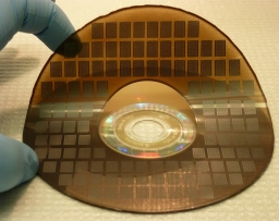
Group NanoXplore Inc., a Montreal-based company specialising in the production and application of graphene and its derivative materials, announced today that it is producing Graphene Oxide in industrial quantities. The Graphene Oxide is being produced in the same 3 metric tonne per year facility used to manufacture NanoXplore’s standard graphene grades and derivative products such as a unique graphite-graphene composite suitable for anodes in Li-ion batteries.

An April 16, 2015 NanoXplore news release on MarketWired, which originated the news item, describes graphene oxide and its various uses,

Graphene Oxide (GO) is similar to graphene but with significant amounts of oxygen introduced into the graphene structure. GO, unlike graphene, can be readily mixed in water which has led people to use GO in thin films, water-based paints and inks, and biomedical applications. GO is relatively simple to synthesise on a lab scale using a modified Hummers’ method, but scale-up to industrial production is quite challenging and dangerous. This is because the Hummers’ method uses strong oxidizing agents in a highly exothermic reaction which produces toxic and explosive gas. NanoXplore has developed a completely new and different approach to producing GO based upon its proprietary graphene production platform. This novel production process is completely safe and environmentally friendly and produces GO in volumes ranging from kilogram to tonne quantities.

“NanoXplore’s ability to produce industrially useful quantities of Graphene Oxide in a safe and scalable manner is a game changer, said Dr. Soroush Nazarpour, President and CEO of NanoXplore. “Mixing graphene with standard industrially materials is the key to bringing it to industrial markets. Graphene Oxide mixes extremely well with all water based solutions, and we have received repeated customer requests for water soluble graphene over the last two years”.

It sounds exciting but it would be helpful (for someone like me, who’s ignorant about these things) to know the graphene oxide market’s size. This would help me to contextualize the excitement.

You can find out more about NanoXplore here.

Converting light to electricity at femto speeds

This is a pretty remarkable (to me anyway) piece of research on speeding up the process of converting light to electricity. From an April 14, 2015 Institute of Photonic Science press release (also on EurekAlert but dated April 15, 2015),

The efficient conversion of light into electricity plays a crucial role in many technologies, ranging from cameras to solar cells. It also forms an essential step in data communication applications, since it allows for information carried by light to be converted into electrical information that can be processed in electrical circuits. Graphene is an excellent material for ultrafast conversion of light to electrical signals, but so far it was not known how fast graphene responds to ultrashort flashes of light.

The new device that the researchers developed is capable of converting light into electricity in less than 50 femtoseconds (a twentieth of a millionth of a millionth of a second). To do this, the researchers used a combination of ultrafast pulse-shaped laser excitation and highly sensitive electrical readout. As Klaas-Jan Tielrooij comments, “the experiment uniquely combined the ultrafast pulse shaping expertise obtained from single molecule ultrafast photonics with the expertise in graphene electronics. Facilitated by graphene’s nonlinear photo-thermoelectric response, these elements enabled the observation of femtosecond photodetection response times.”

The ultrafast creation of a photovoltage in graphene is possible due to the extremely fast and efficient interaction between all conduction band carriers in graphene. This interaction leads to a rapid creation of an electron distribution with an elevated electron temperature. Thus, the energy absorbed from light is efficiently and rapidly converted into electron heat. Next, the electron heat is converted into a voltage at the interface of two graphene regions with different doping. This photo-thermoelectric effect turns out to occur almost instantaneously, thus enabling the ultrafast conversion of absorbed light into electrical signals. As Prof. van Hulst states, “it is amazing how graphene allows direct non-linear detecting of ultrafast femtosecond (fs) pulses”.

The results obtained from the findings of this work, which has been partially funded by the EC Graphene Flagship, open a new pathway towards ultra-fast optoelectronic conversion. As Prof. Koppens comments, “Graphene photodetectors keep showing fascinating performances addressing a wide range of applications”.

Here’s a link to and a citation for the paper,

Generation of photovoltage in graphene on a femtosecond timescale through efficient carrier heating by K. J. Tielrooij, L. Piatkowski, M. Massicotte, A. Woessner, Q. Ma, Y. Lee,  K. S. Myhro, C. N. Lau, P. Jarillo-Herrero, N. F. van Hulst & F. H. L. Koppens. Nature Nanotechnology (2015) doi:10.1038/nnano.2015.54 Published online 13 April 2015

This paper is behind a paywall but there is a free preview via ReadCube Access.

Carbon nanotube commercialization report from the US National Nanotechnology Initiative

Apparently a workshop on the topic commercializing carbon nanotubes was held in Washington, DC. in Sept. 2014. A March 12, 2015 news item on Nanowerk (originated by  March 12, 2015 US National Nanotechnology Initiative news release on EurekAlert) announces the outcome of that workshop (Note: Links have been removed),

The National Nanotechnology Initiative today published the proceedings of a technical interchange meeting on “Realizing the Promise of Carbon Nanotubes: Challenges, Opportunities, and the Pathway to Commercialization” (pdf), held at the National Aeronautics and Space Administration (NASA) Headquarters on September 15, 2014. This meeting brought together some of the Nation’s leading experts in carbon nanotube materials to identify, discuss, and report on technical barriers to the production of carbon nanotube (CNT)-based bulk and composite materials with properties that more closely match those of individual CNTs and to explore ways to overcome these barriers.

The outcomes of this meeting, as detailed in this report, will help inform the future directions of the NNI Nanotechnology Signature Initiative “Sustainable Nanomanufacturing: Creating the Industries of the Future”, which was launched in 2010 to accelerate the development of industrial-scale methods for manufacturing functional nanoscale systems.

The Technical Interchange Proceedings ‘Realizing the Promise of Carbon Nanotubes: Challenges, Opportunities, and the Pathway to Commercialization‘ (30 pp. PDF) describes areas for improvement in its executive summary,

A number of common themes and areas requiring focused attention were identified:

● Increased efforts devoted to manufacturing, quality control, and scale-up are needed. The development of a robust supply of CNT bulk materials with well-controlled properties would greatly enhance commercialization and spur use in a broad range of applications.
● Improvements are needed in the mechanical and electrical properties of CNT-based bulk materials (composites, sheets, and fibers) to approach the properties of individual CNTs. The development of bulk materials with properties nearing ideal CNT values would accelerate widespread adoption of these materials.
● More effective use of simulation and modeling is needed to provide insight into the fundamentals of the CNT growth process. Theoretical insight into the fundamentals of the growth process will inform the development of processes capable of producing high-quality material in quantity.
● Work is needed to help develop an understanding of the properties of bulk CNT-containing materials at longer length scales. Longer length scale understanding will enable the development of predictive models of structure–process–properties relationships and structural design technology tailored to take advantage of CNT properties.
● Standard materials and protocols are needed to guide the testing of CNT-based products for commercial applications. Advances in measurement methods are also required to characterize bulk CNT material properties and to understand the mechanism(s) of failure to help ensure material reliability.
● Life cycle assessments are needed for gauging commercial readiness. Life cycle assessments should include energy usage, performance lifetime, and degradation or disposal of CNT-based products.
● Collaboration to leverage resources and expertise is needed to advance commercialization of CNT-based products. Coordinated, focused efforts across academia, government laboratories, and industry to target grand challenges with support from public–private partnerships would accelerate efforts to provide solutions to overcome these technical barriers.

This meeting identified a number of the technical barriers that need to be overcome to make the promise of carbon nanotubes a reality. A more concerted effort is needed to focus R&D activities towards addressing these barriers and accelerating commercialization. The outcomes from this meeting will inform the future directions of the NNI Nanomanufacturing Signature Initiative and provide specific areas that warrant broader focus in the CNT research community. [p. vii print; p. 9 PDF]

This report, in its final section, explains the basis for the interest in and the hopes for carbon nanotubes,

Improving the electrical and mechanical properties of bulk carbon nanotube materials (yarns, fibers, wires, sheets, and composites) to more closely match those of individual carbon nanotubes will enable a revolution in materials that will have a broad impact on U.S. industries, global competitiveness, and the environment. Use of composites reinforced with high-strength carbon nanotube fibers in terrestrial and air transportation vehicles could enable a 25% reduction in their overall weight, reduce U.S. oil consumption by nearly 6 million barrels per day by 2035 [42], and reduce worldwide consumption of petroleum and other liquid fuels by 25%. This would result in the reduction of CO2 emissions by as much as 3.75 billion metric tons per year. Use of carbon nanotube-based data and power cables would lead to further reductions in vehicle weight, fuel consumption, and CO2 emissions. For example, replacement of the copper wiring in a Boeing 777 with CNT data and power cables that are 50% lighter would enable a 2,000-pound reduction in airplane weight. Use of carbon nanotube wiring in power distribution lines would reduce transmission losses by approximately 41 billion kilowatt hours annually [42], leading to significant savings in coal and gas consumption and reductions in the electric power industry’s carbon footprint.

The impact of developing these materials on U.S. global competitiveness is also significant. For example, global demand for carbon fibers is expected to grow from 46,000 metric tons per year in 2011 to more than 153,000 metric tons in 2020 due to the exponential growth in the use of composites in commercial aircraft, automobiles, aerospace, and wind energy [43]. Ultrahigh-strength CNT fibers would be highly attractive in each of these applications because they offer the advantage of reduced weight and improved performance over conventional carbon fibers. [p. 10 print; p. 20 PDF]

As these things go, this is a very short document, which makes it a fast read, and it has a reference list, something I always find useful.

My colleague, Dexter Johnson in a March 17, 2015 posting on his Nanoclast blog (on the IEEE [Institute for Electrical and Electronics Engineers] website) provides some background information before launching into an analysis of the report’s recommendations (Note: Links have been removed),

In the last half-a-decade we have witnessed once-beloved carbon nanotubes (CNTs) slowly being eclipsed by graphene as the “wonder material” of the nanomaterial universe.

This changing of the guard has occurred primarily within the research community, where the amount of papers being published about graphene seems to be steadily increasing. But in terms of commercial development, CNTs still have a leg up on graphene, finding increasing use in creating light but strong composites. Nonetheless, the commercial prospects for CNTs have been taking hits recently, with some producers scaling down capacity because of lack of demand.

With this as the backdrop, the National Nanotechnology Initiative (NNI), famous for its estimate back in 2001 that the market for nanotechnology will be worth $1 trillion by 2015,  has released a report based on a meeting held last September. …

I recommend reading Dexter’s analysis.

Cute, adorable roundworms help measure nanoparticle toxicity

Caption: Low-cost experiments to test the toxicity of nanomaterials focused on populations of roundworms. Rice University scientists were able to test 20 nanomaterials in a short time, and see their method as a way to determine which nanomaterials should undergo more extensive testing. Credit: Zhong Lab/Rice University

Caption: Low-cost experiments to test the toxicity of nanomaterials focused on populations of roundworms. Rice University scientists were able to test 20 nanomaterials in a short time, and see their method as a way to determine which nanomaterials should undergo more extensive testing.
Credit: Zhong Lab/Rice University

Until now, ‘cute’ and ‘adorable’ are not words I would have associated with worms of any kind or with Rice University, for that matter. It’s amazing what a single image can do, eh?

A Feb. 3, 2015 news item on Azonano describes how roundworms have been used in research investigating the toxicity of various kinds of nanoparticles,

The lowly roundworm is the star of an ambitious Rice University project to measure the toxicity of nanoparticles.

The low-cost, high-throughput study by Rice scientists Weiwei Zhong and Qilin Li measures the effects of many types of nanoparticles not only on individual organisms but also on entire populations.

A Feb. 2, 2015 Rice University news release (also on EurekAlert), which originated the news item, provides more details about the research,

The Rice researchers tested 20 types of nanoparticles and determined that five, including the carbon-60 molecules (“buckyballs”) discovered at Rice in 1985, showed little to no toxicity.

Others were moderately or highly toxic to Caenorhabditis elegans, several generations of which the researchers observed to see the particles’ effects on their health.

The results were published by the American Chemical Society journal Environmental Sciences and Technology. They are also available on the researchers’ open-source website.

“Nanoparticles are basically new materials, and we don’t know much about what they will do to human health and the health of the ecosystem,” said Li, an associate professor of civil and environmental engineering and of materials science and nanoengineering. “There have been a lot of publications showing certain nanomaterials are more toxic than others. So before we make more products that incorporate these nanomaterials, it’s important that we understand we’re not putting anything toxic into the environment or into consumer products.

“The question is, How much cost can we bear?” she said. “It’s a long and expensive process to do a thorough toxicological study of any chemical, not just nanomaterials.” She said that due to the large variety of nanomaterials being produced at high speed and at such a large scale, there is “an urgent need for high-throughput screening techniques to prioritize which to study more extensively.”

Rice’s pilot study proves it is possible to gather a lot of toxicity data at low cost, said Zhong, an assistant professor of biosciences, who has performed extensive studies on C. elegans, particularly on their gene networks. Materials alone for each assay, including the worms and the bacteria they consumed and the culture media, cost about 50 cents, she said.

The researchers used four assays to see how worms react to nanoparticles: fitness, movement, growth and lifespan. The most sensitive assay of toxicity was fitness. In this test, the researchers mixed the nanoparticles in solutions with the bacteria that worms consume. Measuring how much bacteria they ate over time served as a measure of the worms’ “fitness.”

“If the worms’ health is affected by the nanoparticles, they reproduce less and eat less,” Zhong said. “In the fitness assay, we monitor the worms for a week. That is long enough for us to monitor toxicity effects accumulated through three generations of worms.” C. elegans has a life cycle of about three days, and since each can produce many offspring, a population that started at 50 would number more than 10,000 after a week. Such a large number of tested animals also enabled the fitness assay to be highly sensitive.

The researchers’ “QuantWorm” system allowed fast monitoring of worm fitness, movement, growth and lifespan. In fact, monitoring the worms was probably the least time-intensive part of the project. Each nanomaterial required specific preparation to make sure it was soluble and could be delivered to the worms along with the bacteria. The chemical properties of each nanomaterial also needed to be characterized in detail.

The researchers studied a representative sampling of three classes of nanoparticles: metal, metal oxides and carbon-based. “We did not do polymeric nanoparticles because the type of polymers you can possibly have is endless,” Li explained.

They examined the toxicity of each nanoparticle at four concentrations. Their results showed C-60 fullerenes, fullerol (a fullerene derivative), titanium dioxide, titanium dioxide-decorated nanotubes and cerium dioxide were the least damaging to worm populations.

Their “fitness” assay confirmed dose-dependent toxicity for carbon black, single- and multiwalled carbon nanotubes, graphene, graphene oxide, gold nanoparticles and fumed silicon dioxide.

They also determined the degree to which surface chemistry affected the toxicity of some particles. While amine-functionalized multiwalled nanotubes proved highly toxic, hydroxylated nanotubes had the least toxicity, with significant differences in fitness, body length and lifespan.

A complete and interactive toxicity chart for all of the tested materials is available online.

Zhong said the method could prove its worth as a rapid way for drug or other companies to narrow the range of nanoparticles they wish to put through more expensive, dedicated toxicology testing.

“Next, we hope to add environmental variables to the assays, for example, to mimic ultraviolet exposure or river water conditions in the solution to see how they affect toxicity,” she said. “We also want to study the biological mechanism by which some particles are toxic to worms.”

Here’s a citation for the paper and links to the paper and to the researchers’ website,

A multi-endpoint, high-throughput study of nanomaterial toxicity in Caenorhabditis elegans by Sang-Kyu Jung, Xiaolei Qu, Boanerges Aleman-Meza, Tianxiao Wang, Celeste Riepe, Zheng Liu, Qilin Li, and Weiwei Zhong. Environ. Sci. Technol., Just Accepted Manuscript DOI: 10.1021/es5056462 Publication Date (Web): January 22, 2015
Copyright © 2015 American Chemical Society

Nanomaterial effects on C. elegans

Home | Download | Tutorial | About

This heat map indicates whether a measurement for the nanomaterial-exposed worms is higher (yellow), or lower (blue) than the control worms. Black indicates no effects from nanomaterial exposure.

Clicking on colored blocks to see detailed experimental data.

The published paper is open access but you need an American Chemical Society site registration to access it. The researchers’ site is open access.

Nanoelectronics at the University of British Columbia (UBC located in Vancouver, Canada)

Hidden in a Jan. 9, 2014 University of British Columbia (UBC) announcement abut funding from Canada’s Natural Sciences and Engineering Research Council (NSERC) was some information about a nano electronics laboratory,

  • Flexible, efficient solar-battery nano-textile, led by Peyman Servati, funded for $514,000.
  • Bio-inspired soft epidermal and wearable nanofiber electronics for wireless health monitoring, led by Peyman Servati, funded for $516,000. [emphases mine]

Peryman Servati leads FEEL, the flexible electronics and energy lab according to his faculty bio page. The two FEEL project s listed in the announcement have received a total of $1.3* (corrected to $1.03M, Jan. 30, 2014) in funding, over 1/3* (it’s closer to 1/4; corrected Jan. 30, 2014)  of the $4.3M earmarked* (spelling corrected Jan. 30, 2014) for nine UBC projects. Here’s more about the lab’s current roster of four ‘research areas’ from the Research Projects webpage,

1. Transparent Electrodes for Photovoltaic (PV) Devices:

Solar energy, as a clean and renewable resource, is heavily untapped, mainly due to the high cost (>$2 per watt) and low conversion efficiency (~20% for silicon) of today’s PV devices. This project aims at reducing the manufacturing cost of PV devices, by finding a scalable transparent electrode for replacing metal fingers or indium tin oxide (ITO) electrodes of conventional devices. We deposit nanocomposite fibers (NFs) with embedded conductive nanotubes (NTs) and nanowires (NWs) using novel electrospinning process that provides multiscale ordering and alignment in the structure of the NF mesh, similar to veins of a leaf (below). The process is scalable to substrates including plastic, paper and fabric, in a roll-to-roll manufacturing system. Challenges for integration of the NF mesh with Si and thin-film PV panels are being investigated to achieve the required properties at low cost.

2. Nanowire (NW) Growth and Device Fabrication:

Semiconductor and metallic NWs have unique electrical and optical properties not present in the bulk. We grow different NWs with controlled morphology using chemical vapour deposition and other growth techniques. We also work on integration of these nanomaterials into large area electronic devices, including transistors, strain sensors, bio-sensors, photodetectors, and solar cells. Materials of interest include Si, Ge, ZnO, and GaAs.

3. Flexible Organic Solar Cells:

Organic semiconductors can be deposited at low temperature on a variety of substrates. We investigate the aging and annealing effects in these materials and how the morphology of these semiconductors and blends change with time. The goal is to improve efficiency and stability of these devices.

4. Modeling of Nanomaterials and Nanocomposites:

We investigate the electron transport and band structure of novel electronic materials such as nanowires, nanotubes and graphene using atomistic modeling and simulation. [emphasis mine] Our work points out the delicacy of the surface properties of silicon nanowires (NWs) (below) and the dependence of electronic properties on surface composition and reconstruction. In addition, we work on developing analytical models that connect properties of single nanostrucutres to the properties of materials and devices made by using a large number of these nanostrucutures.

My guess is that the two projects which have received money are being investigated via the lab’s four ‘research areas’.

I am glad to have found this nanoeletronics laboratory. Sadly, they’re not investigating the memristors which so fascinate me but I can now say with certainty that there’s at least one laboratory in Canada researching, the world’s currently trendiest nanomaterial, graphene.

Graphene and your sex life

This is a first, as far as I know, for graphene, which is usually discussed in the context of electronics. A research team at the University of Manchester (where it was first isolated by Andre Gerim and Kostya Novoselov in 2004) has won a research grant to develop condoms made of graphere, from the Nov. 22, 2013 news item on Azonano,

Wonder material graphene faces its stiffest challenge yet – providing thinner, stronger, safer and more desirable condoms.

Dr Aravind Vijayaraghavan and his team from The University of Manchester have received a Grand Challenges Explorations grant of $100,000 (£62,123) from the Bill and Melinda Gates Foundation to develop new composite nano-materials for next-generation condoms, containing graphene.

Dr Vijayaraghavan took on a challenge that had been presented to inventors around the world– to develop new technology that would make the condom more desirable for use, which could lead to an increase in condom use.

Here’s how the challenge was presented in March 2013 (from the Develop the Next Generation of Condom challenge webpage on the Grand Challenges (the Bill & Melinda Gates Foundation) website,

Male condoms are cheap, easy to manufacture, easy to distribute, and available globally, including in resource poor settings, through numerous well developed distribution channels.  The current rate of global production is 15 billion units/year with an estimated 750 million users and a steadily growing market. …

The one major drawback to more universal use of male condoms is the lack of perceived incentive for consistent use. The primary drawback from the male perspective is that condoms decrease pleasure as compared to no condom, creating a trade-off that many men find unacceptable, particularly given that the decisions about use must be made just prior to intercourse. …

Likewise, female condoms can be an effective method for prevention of unplanned pregnancy or HIV infection, but suffer from some of the same liabilities as male condoms, require proper insertion training and are substantially more expensive than their male counterparts. …

The Challenge: 

Condoms have been in use for about 400 years yet they have undergone very little technological improvement in the past 50 years. The primary improvement has been the use of latex as the primary material and quality control measures which allow for quality testing of each individual condom. Material science and our understanding of neurobiology has undergone revolutionary transformation in the last decade yet that knowledge has not been applied to improve the product attributes of one of the most ubiquitous and potentially underutilized products on earth. New concept designs with new materials can be prototyped and tested quickly.  Large-scale human clinical trials are not required. Manufacturing capacity, marketing, and distribution channels are already in place.

We are looking for a Next Generation Condom that significantly preserves or enhances pleasure, in order to improve uptake and regular use. Additional concepts that might increase uptake include attributes that increase ease-of-use for male and female condoms, for example better packaging or designs that are easier to properly apply. In addition, attributes that address and overcome cultural barriers are also desired.  Proposals must (i) have a testable hypothesis, (ii) include an associated plan for how the idea would be tested or validated, and (iii) yield interpretable and unambiguous data in Phase I, in order to be considered for Phase II funding.

A few examples of work that would be considered for funding:

  • Application of safe new materials that may preserve or enhance sensation;
  • Development and testing of new condom shapes/designs that may provide an improved user experience;
  • Application of knowledge from other fields (e.g. neurobiology, vascular biology) to new strategies for improving condom desirability.

The project’s team leader, Dr Vijayaraghavan had a few things to say about the possibilities for this composite material (graphene and latex) they are hoping to develop (from the Nov. 21, 2013 University of Manchester news release, which originated the news item on Azonano),

Dr Vijayaraghavan said: “This composite material will be tailored to enhance the natural sensation during intercourse while using a condom, which should encourage and promote condom use.

“This will be achieved by combining the strength of graphene with the elasticity of latex, to produce a new material which can be thinner, stronger, more stretchy, safer and, perhaps most importantly, more pleasurable.”

He also comments on the impact of this project: “Since its isolation in 2004, people have wondered when graphene will be used in our daily life. Currently, people imagine using graphene in mobile-phone screens, food packaging, chemical sensors, etc.

“If this project is successful, we might have a use for graphene which will literally touch our every-day life in the most intimate way.”

I wonder who will be testing these condoms when the time comes.

For anyone who wants to know more about the graphene story, there are these postings (excerpted from my Jan. 3, 2012 posting about their then newly acquired knighthoods): regarding Geim and Novoselov’s work and their Nobel prizes, “my Oct. 7, 2010 posting, which also features a video of a levitating frog (one of Geim’s favourite science stunts) and my Nov. 26, 2010 posting features a video demonstrating how you can make your own graphene sheets.”

One final note, I posted about the Canadian Grand Challenges funding (not be contused with the US-based Bill and Melinda Gates Foundation programme) in this Nov. 21, 2013 posting.

University of Cambridge makes waves with graphene piano

The news about the graphene piano (and anti-fraud lasers, etc.) is contained in a report from the University of Cambridge’s Cambridge Innovation and Knowledge Centre (CIKC), according to a Nov. 5, 2013 news item on phys.org (Note: A link has been removed),

Two prototypes – a detection device which users lasers to fight fraud, and a piano which demonstrates the potential of printed electronics – have been unveiled by Cambridge researchers.

A detection device which uses printed lasers to identify counterfeit goods has been developed by researchers, who say that it could help to make products more resistant to fraud.

The detector is one of a number of innovations covered in a new report by the Cambridge Innovation and Knowledge Centre (CIKC), which has been developing advanced manufacturing technologies for photonics and electronics.

The same document also outlines a new method for printing graphene, showing how the one atom-thick material could be used to make cheap, printed electronics. Using a graphene-based ink, researchers have demonstrated this by creating a transparent, flexible piano.

Here’s a video about the transparent piano produced at Cambridge,

The Nov. 5, 2013 University of Cambridge news release, which originated the news item, offers details about the piano and the graphene inks used to produce it,

The printed piano meanwhile demonstrates the potential of using graphene in real applications where printed electronics might be needed – such as heart monitors and other sensors.

The research team behind it, Drs Tawfique Hasan, Felice Torrisi and Prof Andrea Ferrari, at the Cambridge Graphene Centre, have developed a graphene-based ink. Like the material itself, this has a number of interesting properties, including flexibility, optical transparency, and electrical conductivity.

Other conductive inks are made from precious metals such as silver, which makes them very expensive to produce and process, whereas graphene is both cheap, environmentally stable, and does not require much processing after printing. Graphene ink is also superior to conductive polymers in terms of cost, stability and performance.

The piano, designed in collaboration with Novalia Limited, shows off the graphene ink’s potential. The keys of the transparent piano are made from graphene-based inks, which have been printed on to a plastic film. These keys, working as electrodes, are connected to a simple electronic circuit-board, a battery and speaker. When a person touches a graphene electrode, the amount of electrical charge held in the key changes. This is then detected and redirected by the circuit to the speaker, creating the musical note.

The same research team, in collaboration with Printed Electronics Limited, has developed a flexible prototype digital display. This display uses conventional printable materials, but with a transparent, electrically conductive graphene layer on top. The graphene layer is not only a flexible but also more conductive and transparent than the conventional polymer it replaces. These simple displays can be used in a wide range of smart packaging applications such as toys, labelling and board games.

“Both of these devices show how graphene could be printed on to a whole range of surfaces, which makes it ideal for printed electronics,” Dr Hasan, the lead researcher behind the prototypes, said. For example, it might eventually be possible to print electronics on to clothing and to make wearable patches to monitor people with health conditions, such as a heart problem.”

Another potential application is cheap, printable sensors, which could be used to track luggage around an airport to ensure it is loaded on to the correct plane, or to follow products across a production and supply chain.

For anyone who’d like to see the report and get information on the other projects discussed in it just click on the title: Advanced Manufacturing Technologies for Photonics and Electronics – Exploiting Molecular and Macromolecular Materials: Final Report.

*’Unviersity in headline changed to University 11:11 am PDT Nov. 7, 2013.

Should October 2013 be called ‘the month of graphene’?

Since the Oct. 10-11, 2013 Graphene Flagship (1B Euros investment) launch, mentioned in my preview Oct. 7, 2013 posting, there’ve been a flurry of graphene-themed news items both on this blog and elsewhere and I’ve decided to offer a brief roundup what I’ve found elsewhere.

Dexter Johnson offers a commentary in the pithily titled, Europe Invests €1 Billion to Become “Graphene Valley,” an Oct. 15, 2013 posting on his Nanoclast blog (on the IEEE [Institute of Electrical and Electronics Engineers] website) Note: Links have been removed,

The initiative has been dubbed “The Graphene Flagship,” and apparently it is the first in a number of €1 billion, 10-year plans the EC is planning to launch. The graphene version will bring together 76 academic institutions and industrial groups from 17 European countries, with an initial 30-month-budget of €54M ($73 million).

Graphene research is still struggling to find any kind of applications that will really take hold, and many don’t expect it will have a commercial impact until 2020. What’s more, manufacturing methods are still undeveloped. So it would appear that a 10-year plan is aimed at the academic institutions that form the backbone of this initiative rather than commercial enterprises.

Just from a political standpoint the choice of Chalmers University in Sweden as the base of operations for the Graphene Flagship is an intriguing choice. …

I have to agree with Dexter that choosing Chalmers University over the University of Manchester where graphene was first isolated is unexpected. As a companion piece to reading Dexter’s posting in its entirety and which features a video from the flagship launch, you might want to try this Oct. 15, 2013 article by Koen Mortelmans for Youris (h/t Oct. 15, 2013 news item on Nanowerk),

Andre Konstantin Geim is the only person who ever received both a Nobel and an Ig Nobel. He was born in 1958 in Russia, and is a Dutch-British physicist with German, Polish, Jewish and Ukrainian roots. “Having lived and worked in several European countries, I consider myself European. I don’t believe that any further taxonomy is necessary,” he says. He is now a physics professor at the University of Manchester. …

He shared the Noble [Nobel] Prize in 2010 with Konstantin Novoselov for their work on graphene. It was following on their isolation of microscope visible grapheme flakes that the worldwide research towards practical applications of graphene took off.  “We did not invent graphene,” Geim says, “we only saw what was laid up for five hundred year under our noses.”

Geim and Novoselov are often thought to have succeeded in separating graphene from graphite by peeling it off with ordinary duct tape until there only remained a layer. Graphene could then be observed with a microscope, because of the partial transparency of the material. That is, after dissolving the duct tape material in acetone, of course. That is also the story Geim himself likes to tell.

However, he did not use – as the urban myth goes – graphite from a common pencil. Instead, he used a carbon sample of extreme purity, specially imported. He also used ultrasound techniques. But, probably the urban legend will survive, as did Archimedes’ bath and Newtons apple. “It is nice to keep some of the magic,” is the expression Geim often uses when he does not want a nice story to be drowned in hard facts or when he wants to remain discrete about still incomplete, but promising research results.

Mortelmans’ article fills in some gaps for those not familiar with the graphene ‘origins’ story while Tim Harper’s July 22, 2012 posting on Cientifica’s (an emerging technologies consultancy where Harper is the CEO and founder) TNT blog offers an insight into Geim’s perspective on the race to commercialize graphene with a paraphrased quote for the title of Harper’s posting, “It’s a bit silly for society to throw a little bit of money at (graphene) and expect it to change the world.” (Note: Within this context, mention is made of the company’s graphene opportunities report.)

With all this excitement about graphene (and carbon generally), the magazine titled Carbon has just published a suggested nomenclature for 2D carbon forms such as graphene, graphane, etc., according to an Oct. 16, 2013 news item on Nanowerk (Note: A link has been removed),

There has been an intense research interest in all two-dimensional (2D) forms of carbon since Geim and Novoselov’s discovery of graphene in 2004. But as the number of such publications rise, so does the level of inconsistency in naming the material of interest. The isolated, single-atom-thick sheet universally referred to as “graphene” may have a clear definition, but when referring to related 2D sheet-like or flake-like carbon forms, many authors have simply defined their own terms to describe their product.

This has led to confusion within the literature, where terms are multiply-defined, or incorrectly used. The Editorial Board of Carbon has therefore published the first recommended nomenclature for 2D carbon forms (“All in the graphene family – A recommended nomenclature for two-dimensional carbon materials”).

This proposed nomenclature comes in the form of an editorial, from Carbon (Volume 65, December 2013, Pages 1–6),

All in the graphene family – A recommended nomenclature for two-dimensional carbon materials

  • Alberto Bianco
    CNRS, Institut de Biologie Moléculaire et Cellulaire, Immunopathologie et Chimie Thérapeutique, Strasbourg, France
  • Hui-Ming Cheng
    Shenyang National Laboratory for Materials Science, Institute of Metal Research, Chinese Academy of Sciences, 72 Wenhua Road, Shenyang 110016, China
  • Toshiaki Enoki
    Department of Chemistry, Graduate School of Science and Engineering, Tokyo Institute of Technology, Tokyo, Japan
  • Yury Gogotsi
    Materials Science and Engineering Department, A.J. Drexel Nanotechnology Institute, Drexel University, 3141 Chestnut Street, Philadelphia, PA 19104, USA
  • Robert H. Hurt
    Institute for Molecular and Nanoscale Innovation, School of Engineering, Brown University, Providence, RI 02912, USA
  • Nikhil Koratkar
    Department of Mechanical, Aerospace and Nuclear Engineering, The Department of Materials Science and Engineering, Rensselaer Polytechnic Institute, 110 8th Street, Troy, NY 12180, USA
  • Takashi Kyotani
    Institute of Multidisciplinary Research for Advanced Materials, Tohoku University, 2-1-1 Katahira, Aoba-ku, Sendai 980-8577, Japan
  • Marc Monthioux
    Centre d’Elaboration des Matériaux et d’Etudes Structurales (CEMES), UPR-8011 CNRS, Université de Toulouse, 29 Rue Jeanne Marvig, F-31055 Toulouse, France
  • Chong Rae Park
    Carbon Nanomaterials Design Laboratory, Global Research Laboratory, Research Institute of Advanced Materials, Department of Materials Science and Engineering, Seoul National University, Seoul 151-744, Republic of Korea
  • Juan M.D. Tascon
    Instituto Nacional del Carbón, INCAR-CSIC, Apartado 73, 33080 Oviedo, Spain
  • Jin Zhang
    Center for Nanochemistry, College of Chemistry and Molecular Engineering, Peking University, Beijing 100871, China

This editorial is behind a paywall.

Making a graphene micro-supercapacitor with a home DVD burner

Not all science research and breakthroughs require massive investments of money, sometimes all you need is a home DVD burner as this Feb. 19, 2013 news release on EurekAlert notes,

While the demand for ever-smaller electronic devices has spurred the miniaturization of a variety of technologies, one area has lagged behind in this downsizing revolution: energy-storage units, such as batteries and capacitors.

Now, Richard Kaner, a member of the California NanoSystems Institute at UCLA and a professor of chemistry and biochemistry, and Maher El-Kady, a graduate student in Kaner’s laboratory, may have changed the game.

The UCLA researchers have developed a groundbreaking technique that uses a DVD burner to fabricate micro-scale graphene-based supercapacitors — devices that can charge and discharge a hundred to a thousand times faster than standard batteries. These micro-supercapacitors, made from a one-atom–thick layer of graphitic carbon, can be easily manufactured and readily integrated into small devices such as next-generation pacemakers.

The new cost-effective fabrication method, described in a study published this week in the journal Nature Communications, holds promise for the mass production of these supercapacitors, which have the potential to transform electronics and other fields.

“Traditional methods for the fabrication of micro-supercapacitors involve labor-intensive lithographic techniques that have proven difficult for building cost-effective devices, thus limiting their commercial application,” El-Kady said. “Instead, we used a consumer-grade LightScribe DVD burner to produce graphene micro-supercapacitors over large areas at a fraction of the cost of traditional devices. [emphasis mine] Using this technique, we have been able to produce more than 100 micro-supercapacitors on a single disc in less than 30 minutes, using inexpensive materials.”

The University of California at Los Angeles (UCLA) Feb. 19, 2013 news release written by David Malasarn, the origin of the EurekAlert news release, features more information about the process,

The process of miniaturization often relies on flattening technology, making devices thinner and more like a geometric plane that has only two dimensions. In developing their new micro-supercapacitor, Kaner and El-Kady used a two-dimensional sheet of carbon, known as graphene, which only has the thickness of a single atom in the third dimension.
Kaner and El-Kady took advantage of a new structural design during the fabrication. For any supercapacitor to be effective, two separated electrodes have to be positioned so that the available surface area between them is maximized. This allows the supercapacitor to store a greater charge. A previous design stacked the layers of graphene serving as electrodes, like the slices of bread on a sandwich. While this design was functional, however, it was not compatible with integrated circuits.
In their new design, the researchers placed the electrodes side by side using an interdigitated pattern, akin to interwoven fingers. This helped to maximize the accessible surface area available for each of the two electrodes while also reducing the path over which ions in the electrolyte would need to diffuse. As a result, the new supercapacitors have more charge capacity and rate capability than their stacked counterparts.
Interestingly, the researchers found that by placing more electrodes per unit area, they boosted the micro-supercapacitor’s ability to store even more charge.
Kaner and El-Kady were able to fabricate these intricate supercapacitors using an affordable and scalable technique that they had developed earlier. They glued a layer of plastic onto the surface of a DVD and then coated the plastic with a layer of graphite oxide. Then, they simply inserted the coated disc into a commercially available LightScribe optical drive — traditionally used to label DVDs — and took advantage of the drive’s own laser to create the interdigitated pattern. The laser scribing is so precise that none of the “interwoven fingers” touch each other, which would short-circuit the supercapacitor.
“To label discs using LightScribe, the surface of the disc is coated with a reactive dye that changes color on exposure to the laser light. Instead of printing on this specialized coating, our approach is to coat the disc with a film of graphite oxide, which then can be directly printed on,” Kaner said. “We previously found an unusual photo-thermal effect in which graphite oxide absorbs the laser light and is converted into graphene in a similar fashion to the commercial LightScribe process. With the precision of the laser, the drive renders the computer-designed pattern onto the graphite oxide film to produce the desired graphene circuits.”
“The process is straightforward, cost-effective and can be done at home,” El-Kady said. “One only needs a DVD burner and graphite oxide dispersion in water, which is commercially available at a moderate cost.”
The new micro-supercapacitors are also highly bendable and twistable, making them potentially useful as energy-storage devices in flexible electronics like roll-up displays and TVs, e-paper, and even wearable electronics.

The reference to e-paper and roll-up displays calls to mind work being done at Queen’s University (Kingston, Canada) and Roel Vertegaal’s work on bendable, flexible phones and computers (my Jan. 9, 2013 posting). Could this work on micro-supercapacitors have an impact on that work?

Here’s an image (supplied by UCLA) of the micro-supercapacitors ,

Kaner and El-Kady's micro-supercapacitors

Kaner and El-Kady’s micro-supercapacitors

UCLA has  also supplied a video of Kaner and El-Kady discussing their work,

Interestingly this video has been supported by GE (General Electric), a company which seems to be doing a great deal to be seen on the internet these days as per my Feb. 11, 2013 posting titled, Visualizing nanotechnology data with Seed Media Group and GE (General Electric).

Getting back to the researchers, they are looking for industry partners as per Malasarn’s news release.

AAAS 2013 meeting in Boston,US and Canadian research excellence

The 2013 annual meeting for the American Association for the Advancement of Science (AAAS) will be held in Boston, Massachusetts from Feb. 14 – 18, 2013 with a much better theme this year, The Beauty and Benefits of Science, than last year’s, Flattening the World. (It didn’t take much to improve the theme, eh?)

Plenary speakers range from AAAS’s president, William N. Press to Nathan Myhrvold, a venture capitalist to astrophysicist, Robert Kirshner to Cynthia Kenyon, a molecular biologist to Sherry Turkle. From the AAAS webpage describing Turkle’s 2013 plenary lecture,

Sherry Turkle

Abby Rockefeller Mauzé Professor of the Social Studies of Science and Technology in the Program in Science, Technology, and Society, MIT

The Robotic Moment: What Do We Forget When We Talk to Machines?

Dr. Turkle is founder and director of the MIT Initiative on Technology and Self. She received a joint doctorate in sociology and personality psychology from Harvard University and is a licensed clinical psychologist. Her research focuses on the psychology of human relationships with technology, especially in the realm of how people relate to computational objects. She is an expert on mobile technology, social networking, and sociable robotics and a regular media commentator on the social and psychological effects of technology. Her most recent book is Alone Together: Why We Expect More from Technology and Less from Each Other.

Given my experience last year in the 2012 meeting media room, I’m surprised to see a social media session is planned, from the session webpage,

Engaging with Social Media
Communicating Science
Thursday, February 14, 2013: 3:00 PM-4:30 PM
Ballroom A (Hynes Convention Center)

In a constantly changing online landscape, what is the best way for scientists and engineers to engage the public through social media? This session will discuss how people are accessing science information via blogs and social networks and the importance of researchers getting involved directly. [emphasis mine]  Speakers will address the ways that researchers can create meaningful interactions with the public through social media.

Organizer: Cornelia Dean, The New York Times
Co-Organizer: Dennis Meredith, Science Communication Consultant
Moderator: Carl Zimmer, Independent Science Journalist

Speakers:
XXXX Scicurious, Neurotic Physiology
Science Blogging for Fun and Profit
Christie Wilcox, University of Hawaii
Science in a Digital Age
Dominique Brossard, University of Wisconsin
Science and the Public in New Information Environments

I’d love to see how the theme of ‘researcher engaging directly’ gets developed. In theory, I have no problems with the concept. Unfortunately, those words are sometimes code for this perspective, ‘only experts (scientists/accredited journalists) should discuss or write about science’. A couple of quick comments, my Jan. 13, 2012 posting featured an interview with Carl Zimmer, this session’s moderator, about his science tattoo book and Dominique Brossard, one of the speakers, was last mentioned here in my Jan. 24, 2013 posting titled, Tweet your nano, in the context of a research study on social media and nanotechnology.

In keeping with the times (as per my Jan. 28, 2013 posting about the colossal research prizes for the Graphene and Human Brain Project initiatives), the 2012 AAAS annual meeting features a Brain Function and Plasticity thread or subtheme. There’s this session amongst others,

The Connectome: From the Synapse to Brain Networks in Health and Disease
Brain Function and Plasticity
Saturday, February 16, 2013: 8:30 AM-11:30 AM
Room 304 (Hynes Convention Center)

A series of innovative studies are being done to map the brain from the molecular to the systems level both structurally and functionally. At the synaptic level, how neurotransmitters, their receptors, and signaling pathways influence neural function and plasticity is becoming much better understood. Integrating neuronal function at the level of single neurons and groups of neurons into larger circuits at the anatomical level in the mammalian brain, while a daunting task, is being studied by advanced imaging techniques requiring vast amounts of information storage and processing. To integrate local circuit function with whole brain function, understanding the structure and processing of brain networks is critical. A major project to accomplish this task, the Human Connectome Project, is in the process of integrating the structure and function of brain networks using the most advanced imaging and analysis techniques in 1,200 people, including twins and their nontwin siblings. This step will allow for major new insights into not only brain structure and function, but also their genetic underpinnings. Comparing this information in both the normal brain and in different brain disorders such as neurodegenerative diseases is providing novel insights into how understanding brain function from the molecular to the systems level will provide insights into normal brain function and disease pathogenesis as well as provide new treatment strategies.

Organizer:

David Holtzman, Washington University

Speakers:

Mark F. Bear, Massachusetts Institute of Technology
Molecules and Mechanisms Involved in Synaptic Plasticity in Health and Disease
Jeff Lichtman, Harvard University
Connectomics: Developing a Wiring Diagram for the Mammalian Brain
Steve Petersen, Washington University
The Human Connectome Project
Marcus E. Raichle, Washington University
The Brain’s Dark Energy and the Default Mode Network
Nicole Calakos, Duke University
Synaptic Plasticity in the Basal Ganglia in Health and Disease
William W. Seeley, University of California
Brain Networks: Linking Structure and Function in Neurodegenerative Diseases

Then, there’s this session featuring graphene,

What’s Hot in Cold
Sunday, February 17, 2013: 8:30 AM-11:30 AM
Room 308 (Hynes Convention Center)

The study of ultracold atoms and molecules is now the frontier of low-temperature science, reaching temperatures of a few hundred picokelvin above absolute zero. This field was made possible by a technique that did not exist 30 years ago: laser cooling of atoms. It is hardly obvious that the laser, which produces the most intense light on Earth and is routinely used in industrial applications for cutting and welding medal, would also provide the most powerful coolant. Such are the surprises of science, where a breakthrough in one area transforms others in unexpected ways. Since 1997, eight Nobel Laureates in physics have been recognized for contributions to ultracold atomic and molecular science, which has become one of the most vibrant fields in physics, cutting across traditional disciplinary boundaries, e.g., atomic, molecular, and optical; condensed matter; statistical physics; and nuclear and particle physics. This field builds on two accomplishments that it was the first to achieve: first, the production of quantum degenerate matter using a wide range of elements and, second, exquisite control of quantum degenerate matter at the atomic level. These have led to record low temperatures, ultraprecise atomic clocks, and new forms of quantum matter that generalize ideas from magnetism superconductivity and graphene physics.

Organizer:

Charles W. Clark, Joint Quantum Institute

Speakers:

Markus Greiner, Harvard University
Quantum Simulation: A Microscopic View of Quantum Matter
Ana Maria Rey, University of Colorado
Atomic Clocks: From Precise Timekeepers to Quantum Simulators
Daniel Greif, ETH Zurich
Exploring Dirac Points with Ultracold Fermions in a Tunable Honeycomb Lattice
Gretchen Campbell, Joint Quantum Institute
Superflow in Bose-Einstein Condensate Rings: Tunable Weak Links in Atom Circuits
Benjamin Lev, Stanford University
New Physics in Strongly Magnetic Ultracold Gases

Amongst all these other sessions, there’s a session about Canadian science,

Introduction to Canadian Research Excellence: Evidence & Examples
Friday, February 15, 2013: 11:00 AM-12:00 PM
Room 205 (Hynes Convention Center)

The Canada Pavilion in the Exhibit Hall gives a taste of what lies north of Boston and the 49th parallel. Join us at this workshop to learn about opportunities in Canada for research and study. Canada recently completed a comprehensive analysis of its domestic science and technology strengths. The final report of the expert panel of the Council of Canadian Academies will be presented, including the use of global benchmarks and insights on international collaborations. Two of the drivers for Canadian excellence will be introduced: large-scale science facilities in key fields and a system of targeted fellowships and research chairs that recruit globally.

Coordinator:

Tim Meyer, TRIUMF

Presenters:

Tim Meyer, TRIUMF,
Chad Gaffield, Social Sciences and Humanities Research Council of Canada
Eliot Phillipson, University of Toronto

“Introduced,” really? Large scale science facilities are not new in Canada or anywhere else for that matter and the programmes of targeted fellowships have been around long enough and successful enough that it is being copied.

First, there was the Canada Research Chair programme, which was instituted in 2000. From the About Us page (Note: A link has been removed),

The Canada Research Chairs program stands at the centre of a national strategy to make Canada one of the world’s top countries in research and development. [emphasis mine]

In 2000, the Government of Canada created a permanent program to establish 2000 research professorships—Canada Research Chairs—in eligible degree-granting institutions across the country.

The Canada Research Chairs program invests $300 million per year to attract and retain some of the world’s most accomplished and promising minds.

This was programme was followed up with the Canada Excellence Research Chairs Program in 2008, from the Background page (Note: A link has been removed),

Launched in 2008, the Canada Excellence Research Chairs (CERC) Program supports Canadian universities in their efforts to build on Canada’s growing reputation as a global leader in research and innovation. The program awards world-renowned researchers and their teams up to $10 million over seven years to establish ambitious research programs at Canadian universities. These awards are among the most prestigious and generous available globally.

In May 2010, the first group of Canada Excellence Research Chairs was announced. Selected through a rigorous, multilevel peer review process, these chairholders are helping Canada build a critical mass of expertise in the four priority research areas of the federal government’s science and technology strategy …

Here’s an excerpt from my Feb. 21, 2012 posting,

Canadians have been throwing money at scientists for some years now (my May 20, 2010 posting about the Canada Excellence Research Chairs programme). We’ve attempted to recruit from around the world with our ‘research chairs’ and our ‘excellence research chairs’ and our Network Centres of Excellence (NCE) all serving as enticements.

The European Research Council (ERC) has announced that they will be trying to beat us at our own game at the AAAS 2012 annual meeting in Vancouver (this new ERC programme was launched in Boston, Massachusetts in January 2012).

The Canadian report these folks will be discussing was released in Sept. 2012 and was  featured here in a two-part commentary,

The State of Science and Technology in Canada, 2012 report—examined (part 1: the executive summary)

The State of Science and Technology in Canada, 2012 report—examined (part 2: the rest of the report)

My Sept. 27, 2012 posting features my response to the report’s launch on that day.

As for the AAAS 2013 annual meeting, there’s a lot, lot more of it and it’s worth checking out, if for no other reason than to anticipate the types of science stories you will be seeing in the coming months.