Monthly Archives: July 2016

NEC and its ‘carbon nanobrush’

Long associated with the discovery of carbon nanotubes (CNTs), NEC Corporation has announced another carbon material, carbon nanobrushes, in a July 7, 2016 news item on phys.org,

NEC Corporation today [June 30, 2016] announced the discovery of a new nano carbon material, the “carbon nanobrush,” a fibrous aggregate of single-walled carbon nanohorns. Moreover, NEC has become the first company in the world to manufacture the carbon nanobrush.

A June 30, 2016 NEC Corporation press release, which originated the news item, provides more detail (Note: This excerpt has been reformatted for clarity),

“The ‘carbon nanobrush’ is a new nano carbon material that, like existing carbon nanohorns, has high water and solvent dispersity, and high adsorptivity, including substance adsorption, but has more than 10 times the electrical conductivity than existing carbon nanohorns, an important characteristic for industrial applications,” said Dr. Sumio Iijima, Senior Research Fellow, NEC Corporation. “With these characteristics, it is anticipated that the carbon nanobrush will help to improve the basic functionality of a range of devices, including increasing the speed of sensor and actuator responses, improving the output properties of batteries and capacitors, while increasing the electrical conductivity of rubber and plastic composite materials, as well as having application in a wide range of industries.”

1. TEM images of the obtained samples

2. Tips of single-walled carbon nanohorn

3. Spherical-carbon nanohorn aggregates

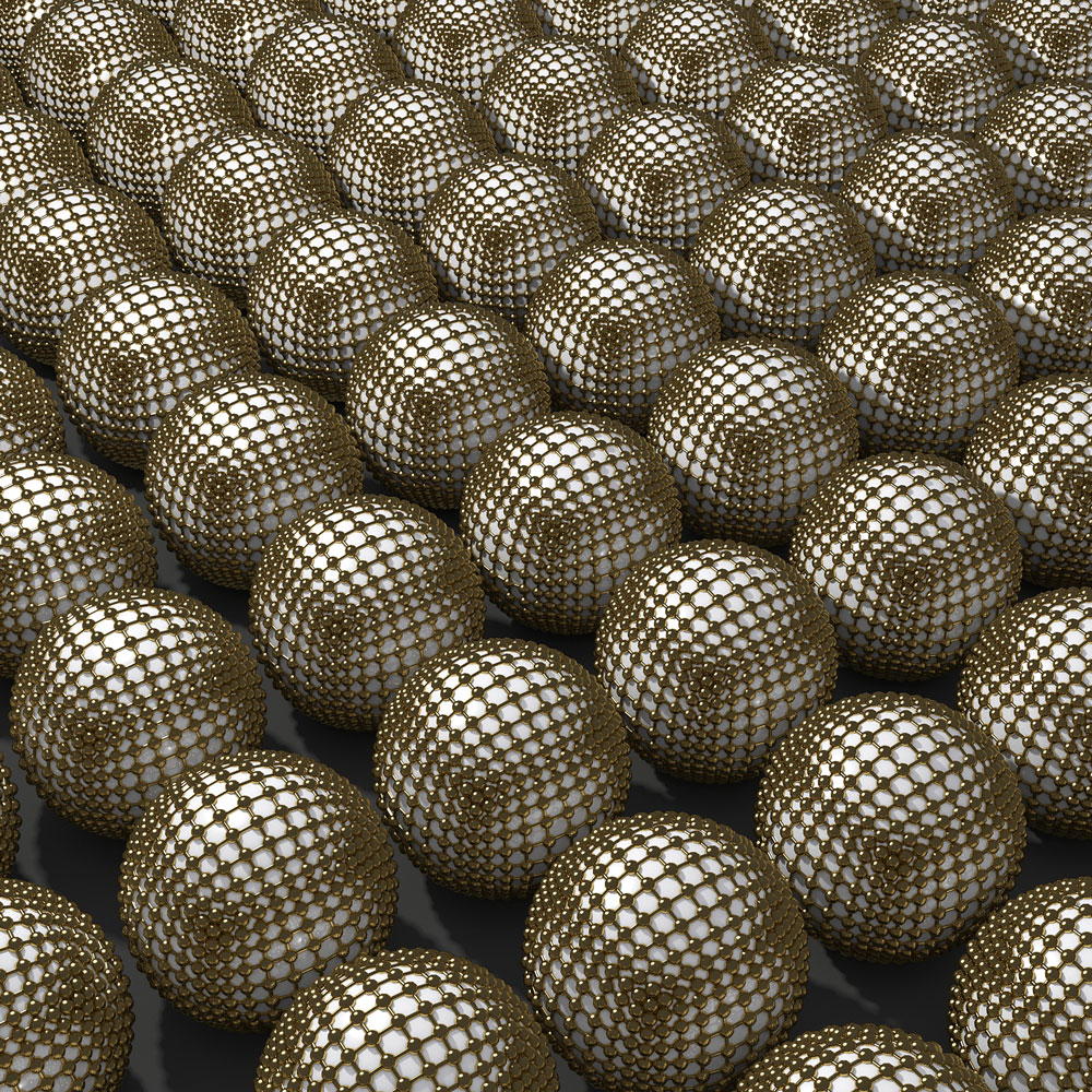
Carbon nanohorns are horn-shaped (figure 2) nano carbon structures 2-5 nanometers (nm) in diameter and 40-50nm in length, which until now have been produced as radial spherical aggregates (figure 3). The newly discovered carbon nanobrush is a uniquely shaped material. It is fibrous aggregates composed of radially-assembled graphene-based single-walled nanotubules, named here as fibrous aggregates of single-walled carbon nanohorns, whose structure resembles that of a round brush (figure 1).

Features of the “carbon nanobrush” include the following:

    1. Structure
      (1)Single-walled carbon nanohorns of 2-5nm in diameter and 40-50nm in length radially gather and are connected fibrously in several micrometers.
      (2)The single-walled carbon nanohorn which is a horn-shaped nano carbon structure with a large surface area radially gather and are connected fibrously in several micrometers. So it has a large surface area per unit mass (up to 1700㎡/g).
    1. Characteristics
      (1)Dispersity
      Like carbon nanohorns, the carbon nanobrush has high dispersibility, dispersing in water and organic solvents, for example. This means that it can be easily mixed with a variety of materials, making it easy to improve its characteristics as a base material.(2)Adsorptivity
      Like spherical carbon nanohorns, the carbon nanobrush can contain various substances in the nano-sized spaces inside the tubular structure, so it can be utilized as a high-performance adsorbent. When holes are formed on the surface of the carbon nanohorns by oxidation treatments, the inner space can be used, expanding the surface area by a factor of approximately five and greatly increasing adsorptivity.

      (3)Electrical conductivity
      As carbon nanobrush is a fibrous aggregate of radially-assembled carbon nanohorns, it has more than 10 times the electrical conductivity compared with existing spherical carbon nanohorn aggregates. As a result, they are highly effective in increasing the speed of sensor and actuator responses, increasing output properties of batteries and capacitors, and increasing the electrical conductivity of rubber and plastic composite materials.

  1. Production process
    Carbon nanobrush can be produced at room temperature and under atmospheric pressure using the laser ablation method where an iron-containing carbon target (mass of carbon) is irradiated by a laser with high power density. The simple production process means that they can be produced efficiently and at a low cost when compared to the cost of other nano carbon materials.

This technology was developed in part through collaborative research with the National Institute of Advanced Industrial Science and Technology (AIST).

Here’s a link to and a citation for the paper,

Preparation and Characterization of Newly Discovered Fibrous Aggregates of Single-Walled Carbon Nanohorns by Ryota Yuge, Fumiyuki Nihey, Kiyohiko Toyama, and Masako Yudasaka. Advanced Materials DOI: 10.1002/adma.201602022 Version of Record online: 25 MAY 2016

© 2016 WILEY-VCH Verlag GmbH & Co. KGaA, Weinheim

This paper is behind a paywall.

For anyone interested in a history of carbon nanotubes, there’s my June 10, 2016 posting: The birth of carbon nanotubes (CNTs): a history, which includes a mention of NEC and its position as the discoverer of carbon nanotubes.

Getting one step closer to molecular robots

A July 5, 2016 news item on ScienceDaily announced research from Hokkaido University (Japan),

Scientists at Japan’s Hokkaido University have developed light-powered molecular motors that repetitively bend and unbend, bringing us closer to molecular robots.

A July 6, 2016 Hokkaido University press release (also on EurekAlert), which originated the news item, expands on the theme,

Researchers are working on mimicking cellular systems to develop molecular motors that can move or even deliver drugs to target tissues. Engineering such motors may ultimately lead to molecular robots that can execute more complex tasks. To this end, researchers must find ways to convert motion at the molecular level to motion at the macroscopic level. They also must find ways to cause chemical reactions to repeat autonomously and continuously.
Yoshiyuki Kageyama, Sadamu Takeda and colleagues at Hokkaido University’s Department of Chemistry have successfully created a chemical compound, or a crystalline assembly, which autonomously repeated flipping under blue light.

The team made crystals composed of an organic compound, called azobenzene, commonly used in dye manufacturing, and oleic acid, commonly found in cooking oil. Azobenzene molecules take two structurally different forms: cis and trans. They repetitively convert from one form to the other under blue right. The scientists tested if this would influence the structure of the azobenzene-oleic acid crystal, which contained unequal amounts of cis– and trans-azobenzene.

By applying blue light to the crystals in solution, the team observed, under a microscope, an oscillatory bending-unbending motion of the thin crystals, suggesting the existence of two stable structures, bent or unbent, depending on the cis/trans ratio. The frequency of the motion increased when the light intensity was increased. Some crystal complexes even exhibited ‘swimming-like’ motions in the water. Previously reported light-responsive materials have been limited in their ability to deform. The properties of the compounds in the Hokkaido University-developed crystals, however, allowed for a two-step switching mechanism, resulting in regular repetitive oscillations.

Schematic illustration of each step of the self-oscillatory motion. (Ikegami T. et. al., Angewandte Chemie International Edition, May 19, 2016)

Schematic illustration of each step of the self-oscillatory motion. (Ikegami T. et. al., Angewandte Chemie International Edition, May 19, 2016)

“The ability to self-organize rhythmic motions, such as the repetitive flipping motion we observed, is one of the fundamental characteristics of living organisms”, says Kageyama. “This mechanism can be used in the future to develop bio-inspired molecular motors and robots that will find applications in wide areas, including medicine”.

You can observe the flipping here in this video provided by Hokkaido University,

Here’s a link to and a citation for the paper,

Dissipative and Autonomous Square-Wave Self-Oscillation of a Macroscopic Hybrid Self-Assembly under Continuous Light Irradiation by Tomonori Ikegami, Dr. Yoshiyuki Kageyama, Kazuma Obara, and Prof. Sadamu Takeda. Angewandte Chemie International Edition Volume 55, Issue 29, pages 8239–8243, July 11, 2016 DOI: 10.1002/anie.201600218 Version of Record online: 19 MAY 2016

© 2016 WILEY-VCH Verlag GmbH & Co. KGaA, Weinheim

This paper is behind a paywall.

Google Arts & Culture: an app for culture vultures

In its drive to take over single aspect of our lives in the most charming, helpful, and delightful ways possible, Google has developed its Arts & Culture app.

Here’s more from a July 19, 2016 article by John Brownlee for Fast Company (Note: Links have been removed),

… Google has just unveiled a new app that makes it as easy to find the opening times of your local museum as it is to figure out who painted that bright purple Impressionist masterpiece you saw five years ago at the Louvre.

It’s called Google Arts & Culture, and it’s a tool for discovering art “from more than a thousand museums across 70 countries,” Google writes on its blog. More than just an online display of art, though, it encourages viewers to parse the works and gather insight into the visual culture we rarely encounter outside the rarified world of brick-and-mortar museums.

For instance, you can browse all of Van Gogh’s paintings chronologically to see how much more vibrant his work became over time. Or you can sort Monet’s paintings by color for a glimpse at his nuanced use of gray.

You can also read daily stories about subjects such as stolen Nazi artworks or Bruegel’s Tower of Babel. …

A July 19, 2016 post announcing the Arts & Culture app on the Google blog by Duncan Osborn provides more details,

Just as the world’s precious artworks and monuments need a touch-up to look their best, the home we’ve built to host the world’s cultural treasures online needs a lick of paint every now and then. We’re ready to pull off the dust sheets and introduce the new Google Arts & Culture website and app, by the Google Cultural Institute. The app lets you explore anything from cats in art since 200 BCE to the color red in Abstract Expressionism, and everything in between.

• Search for anything, from shoes to all things gold • Scroll through art by time—see how Van Gogh’s works went from gloomy to vivid • Browse by color and learn about Monet’s 50 shades of gray • Find a new fascinating story to discover every day—today, it’s nine powerful men in heels

You can also use this app when visiting a real life museum. For the interested, you can download it for for iOS and Android.

Memory material with functions resembling synapses and neurons in the brain

This work comes from the University of Twente’s MESA+ Institute for Nanotechnology according to a July 8, 2016 news item on ScienceDaily,

Our brain does not work like a typical computer memory storing just ones and zeroes: thanks to a much larger variation in memory states, it can calculate faster consuming less energy. Scientists of the MESA+ Institute for Nanotechnology of the University of Twente (The Netherlands) now developed a ferro-electric material with a memory function resembling synapses and neurons in the brain, resulting in a multistate memory. …

A July 8, 2016 University of Twente press release, which originated the news item, provides more technical detail,

The material that could be the basic building block for ‘brain-inspired computing’ is lead-zirconium-titanate (PZT): a sandwich of materials with several attractive properties. One of them is that it is ferro-electric: you can switch it to a desired state, this state remains stable after the electric field is gone. This is called polarization: it leads to a fast memory function that is non-volatile. Combined with processor chips, a computer could be designed that starts much faster, for example. The UT scientists now added a thin layer of zinc oxide to the PZT, 25 nanometer thickness. They discovered that switching from one state to another not only happens from ‘zero’ to ‘one’ vice versa. It is possible to control smaller areas within the crystal: will they be polarized (‘flip’) or not?

In a PZT layer without zinc oxide (ZnO) there are basically two memorystates. Adding a nano layer of ZnO, every state in between is possible as well.

Multistate

By using variable writing times in those smaller areas, the result is that many states can be stored anywhere between zero and one. This resembles the way synapses and neurons ‘weigh’ signals in our brain. Multistate memories, coupled to transistors, could drastically improve the speed of pattern recognition, for example: our brain performs this kind of tasks consuming only a fraction of the energy a computer system needs. Looking at the graphs, the writing times seem quite long compared to nowaday’s processor speeds, but it is possible to create many memories in parallel. The function of the brain has already been mimicked in software like neurale networks, but in that case conventional digital hardware is still a limitation. The new material is a first step towards electronic hardware with a brain-like memory. Finding solutions for combining PZT with semiconductors, or even developing new kinds of semiconductors for this, is one of the next steps.

Here’s a link to and a citation for the paper,

Multistability in Bistable Ferroelectric Materials toward Adaptive Applications by Anirban Ghosh, Gertjan Koster, and Guus Rijnders. Advanced Functional Materials DOI: 10.1002/adfm.201601353 Version of Record online: 4 JUL 2016

© 2016 WILEY-VCH Verlag GmbH & Co. KGaA, Weinheim

This paper is behind a paywall.

Using light to make gold crystal nanoparticles

Gold crystal nanoparticles? Courtesy: University of Florida

Gold crystal nanoparticles? Courtesy: University of Florida

A team from the University of Florida has used gold instead of silver in a process known as plasmon-driven synthesis. From a July 8, 2016 news item on phys.org,

A team of University of Florida researchers has figured out how gold can be used in crystals grown by light to create nanoparticles, a discovery that has major implications for industry and cancer treatment and could improve the function of pharmaceuticals, medical equipment and solar panels.

A July 6, 2016 University of Florida news release, which originated the news item, provides more detail,

Nanoparticles can be “grown” in crystal formations with special use of light, in a process called plasmon-driven synthesis. However, scientists have had limited control unless they used silver, but silver limits the uses for medical technology. The team is the first to successfully use gold, which works well within the human body, with this process.

“How does light actually play a role in the synthesis? [This knowledge] was not well developed,” said David Wei, an associate professor of chemistry who led the research team. “Gold was the model system to demonstrate this.”

Gold is highly desired for nanotechnology because it is malleable, does not react with oxygen and conducts heat well. Those properties make gold an ideal material for nanoparticles, especially those that will be placed in the body.

When polyvinylpyrrolidone, or PVP, a substance commonly found in pharmaceutical tablets, is used in the plasmon-driven synthesis, it enables scientists to better control the growth of crystals. In Wei’s research, PVP surprised the team by showing its potential to relay light-generated “hot” electrons to a gold surface to grow the crystals.

The research describes the first plasmonic synthesis strategy that can make high-yield gold nanoprisms. Even more exciting, the team has demonstrated that visible-range and low-power light can be used in the synthesis. Combined with nanoparticles being used in solar photovoltaic devices, this method can even harness solar energy for chemical synthesis, to make nanomaterials or for general applications in chemistry.

Wei has spent the last decade working in nanotechnology. He is intrigued by its applications in photochemistry and biomedicine, especially in targeted drug delivery and photothermal therapeutics, which is crucial to cancer treatment. His team includes collaborators from Pacific Northwest National Laboratory, where he has worked as a visiting scholar, and Brookhaven National Laboratory. In addition, the project has provided an educational opportunity for chemistry students: one high school student (through UF’s Student Science Training Program), two University scholars who also [sic] funded by the Howard Hughes Medical Institute, five graduate students and two postdocs.

Here’s a link to and a citation for the paper,

Polyvinylpyrrolidone-induced anisotropic growth of gold nanoprisms in plasmon-driven synthesis by Yueming Zhai, Joseph S. DuChene, Yi-Chung Wang, Jingjing Qiu, Aaron C. Johnston-Peck, Bo You, Wenxiao Guo, Benedetto DiCiaccio, Kun Qian, Evan W. Zhao, Frances Ooi, Dehong Hu, Dong Su, Eric A. Stach, Zihua Zhu, & Wei David Wei. Nature Materials (2016) doi:10.1038/nmat4683 Published online 04 July 2016

This paper is behind a paywall.

DNA as a sensor

McMaster University (Ontario, Canada) researchers have developed a technique for using DNA (deoxyribonucleic acid) as a sensor according to a July 7, 2016 news item on ScienceDaily,

Researchers at McMaster University have established a way to harness DNA as the engine of a microscopic “machine” they can turn on to detect trace amounts of substances that range from viruses and bacteria to cocaine and metals.

“It’s a completely new platform that can be adapted to many kinds of uses,” says John Brennan, director of McMaster’s Biointerfaces Insitute and co-author of a paper in the journal Nature Communications that describes the technology. “These DNA nano-architectures are adaptable, so that any target should be detectable.”

A July 7, 2016 McMaster University news release (also on EurekAlert), which originated the news item, expands on the theme,

DNA is best known as a genetic material, but is also a very programmable molecule that lends itself to engineering for synthetic applications.

The new method shapes separately programmed pieces of DNA material into pairs of interlocking circles.

The first remains inactive until it is released by the second, like a bicycle wheel in a lock. When the second circle, acting as the lock, is exposed to even a trace of the target substance, it opens, freeing the first circle of DNA, which replicates quickly and creates a signal, such as a colour change.

“The key is that it’s selectively triggered by whatever we want to detect,” says Brennan, who holds the Canada Research Chair in Bioanalytical Chemistry and Biointerfaces. “We have essentially taken a piece of DNA and forced it to do something it was never designed to do. We can design the lock to be specific to a certain key. All the parts are made of DNA, and ultimately that key is defined by how we build it.”

The idea for the “DNA nanomachine” comes from nature itself, explains co-author Yingfu Li, who holds the Canada Research Chair in Nucleic Acids Research.

“Biology uses all kinds of nanoscale molecular machines to achieve important functions in cells,” Li says. “For the first time, we have designed a DNA-based nano-machine that is capable of achieving ultra-sensitive detection of a bacterial pathogen.”

The DNA-based nanomachine is being further developed into a user-friendly detection kit that will enable rapid testing of a variety of substances, and could move to clinical testing within a year.

Here’s a link to and a citation for the paper,

Programming a topologically constrained DNA nanostructure into a sensor by Meng Liu, Qiang Zhang, Zhongping Li, Jimmy Gu, John D. Brennan, & Yingfu Li. Nature Communications 7, Article number: 12074  doi:10.1038/ncomms12074 Published 23 June 2016

This paper is open access.

Nanotechnology-enhanced roads in South Africa and in Kerala, India

It’s all about road infrastructure in these two news bits.

Road building and maintenance in sub-Saharan Africa

A July 7, 2016 news item on mybroadband.co.za describes hopes that nanotechnology-enabled products will make roads easier to build and maintain,

The solution for affordable road infrastructure development could lie in the use of nanotechnology, according to a paper presented at the 35th annual Southern African Transport Conference in Pretoria.

The cost of upgrading, maintaining and rehabilitating road infrastructure with limited funds makes it impossible for sub-Saharan Africa to become competitive in the world market, according to Professor Gerrit Jordaan of the University of Pretoria, a speaker at the conference.

The affordability of road infrastructure depends on the materials used, the environment in which the road will be built and the traffic that will be using the road, explained Professor James Maina of the department of civil engineering at the University of Pretoria.

Hauling materials to a construction site contributes hugely to costs, which planners try to minimise by getting materials closer to the site. But if there aren’t good quality materials near the site, another option is to modify poor quality materials for construction purposes. This is where nanotechnology comes in, he explained.

For example, if the material is clay soil, it has a high affinity to water so when it absorbs water it expands, and when it dries out it contracts. Nanotechnology can make the soil water repellent. “Essentially, nanotechnology changes the properties to work for the construction process,” he said.

These nanotechnology-based products have been used successfully in many parts of the world, including India, the USA and in the West African region.

There have also been concerns about road building and maintenance in Kerala, India.

Nanotechnology for city roads in Kochi

A March 23, 2015 news item in the Times of India describes an upcoming test of a nanotechnology-enabled all weather road,

Citizens can now look forward to better roads with the local self-government department planning to use nanotechnology to construct all-weather roads.

For the district trial run, the department has selected a 300-metre stretch of a panchayat road in Edakkattuvayal panchayat. The trial would experiment with nanotechnology to build moisture resistant, long-lasting and maintenance-free roads.

“Like the public, the department is also fed up with the poor condition of roads in the state. Crores of rupees are spent every year for repairing and resurfacing the roads. This is because of heavy rains in the state that weakens the soil base of roads, resulting in potholes that affect the ride-quality of the road surface,” said KT Sajan, assistant executive engineer, LSGD, who is supervising the work.

The nanotechnology has been developed by Zydex Technologies, a Gujarat-headquartered firm. The company’s technology has already been used by major private contract firms that build national highways in India and in other major projects in European and African countries.

Oddly, you can’t find out more about the Zydex products mentioned in the article on its Roads Solution webpage , where you are provided a general description of the technology,

Revolutionary nanotechnology for building moisture resistant, long lasting & maintenance free roads through innovative adaptation of Organosilane chemistry.

Zydex Nanotechnology: A Game Changer

Zydex Nanotechnology has a value propositions for all layers of the road

SOIL LAYERS
Zydex Nanotechnology makes the soil moisture resistant, reduces expansiveness and stabilizes the soil to improve its bearing strength manifold. If used with 1% cement, it can stabilize almost any type of soil, by improving the California Bearing Ratio (CBR) to even 100 or above.

Here is the real change in game, as stronger soil bases would now allow optimization of road section thicknesses, potentially saving 10-15% road construction cost.

BOND COATS
Prime & Tack coats become 100 % waterproofed, due to penetration and chemical bonding. This also ensures uniform load transfer. And all this at lower residual bitumen.

ASPHALTIC LAYERS
Chemical bonding between aggregates and asphalt eliminates moisture induced damage of asphaltic layers.

Final comment

I hadn’t meant to wait so long to publish the bit about Kerala’s road but serendipity has allowed me to link it to a piece about South Africa ‘s roads and to note a resemblance to the problems encountered in both regions.

Cornwall (UK) connects with University of Southern California for performance by a quantum computer (D-Wave) and mezzo soprano Juliette Pochin

The upcoming performance of a quantum computer built by D-Wave Systems (a Canadian company) and Welsh mezzo soprano Juliette Pochin is the première of “Superposition” by Alexis Kirke. A July 13, 2016 news item on phys.org provides more detail,

What happens when you combine the pure tones of an internationally renowned mezzo soprano and the complex technology of a $15million quantum supercomputer?

The answer will be exclusively revealed to audiences at the Port Eliot Festival [Cornwall, UK] when Superposition, created by Plymouth University composer Alexis Kirke, receives its world premiere later this summer.

A D-Wave 1000 Qubit Quantum Processor. Credit: D-Wave Systems Inc

A D-Wave 1000 Qubit Quantum Processor. Credit: D-Wave Systems Inc

A July 13, 2016 Plymouth University press release, which originated the news item, expands on the theme,

Combining the arts and sciences, as Dr Kirke has done with many of his previous works, the 15-minute piece will begin dark and mysterious with celebrated performer Juliette Pochin singing a low-pitched slow theme.

But gradually the quiet sounds of electronic ambience will emerge over or beneath her voice, as the sounds of her singing are picked up by a microphone and sent over the internet to the D-Wave quantum computer at the University of Southern California.

It then reacts with behaviours in the quantum realm that are turned into sounds back in the performance venue, the Round Room at Port Eliot, creating a unique and ground-breaking duet.

And when the singer ends, the quantum processes are left to slowly fade away naturally, making their final sounds as the lights go to black.

Dr Kirke, a member of the Interdisciplinary Centre for Computer Music Research at Plymouth University, said:

“There are only a handful of these computers accessible in the world, and this is the first time one has been used as part of a creative performance. So while it is a great privilege to be able to put this together, it is an incredibly complex area of computing and science and it has taken almost two years to get to this stage. For most people, this will be the first time they have seen a quantum computer in action and I hope it will give them a better understanding of how it works in a creative and innovative way.”

Plymouth University is the official Creative and Cultural Partner of the Port Eliot Festival, taking place in South East Cornwall from July 28 to 31, 2016 [emphasis mine].

And Superposition will be one of a number of showcases of University talent and expertise as part of the first Port Eliot Science Lab. Being staged in the Round Room at Port Eliot, it will give festival goers the chance to explore science, see performances and take part in a range of experiments.

The three-part performance will tell the story of Niobe, one of the more tragic figures in Greek mythology, but in this case a nod to the fact the heart of the quantum computer contains the metal named after her, niobium. It will also feature a monologue from Hamlet, interspersed with terms from quantum computing.

This is the latest of Dr Kirke’s pioneering performance works, with previous productions including an opera based on the financial crisis and a piece using a cutting edge wave-testing facility as an instrument of percussion.

Geordie Rose, CTO and Founder, D-Wave Systems, said:

“D-Wave’s quantum computing technology has been investigated in many areas such as image recognition, machine learning and finance. We are excited to see Dr Kirke, a pioneer in the field of quantum physics and the arts, utilising a D-Wave 2X in his next performance. Quantum computing is positioned to have a tremendous social impact, and Dr Kirke’s work serves not only as a piece of innovative computer arts research, but also as a way of educating the public about these new types of exotic computing machines.”

Professor Daniel Lidar, Director of the USC Center for Quantum Information Science and Technology, said:

“This is an exciting time to be in the field of quantum computing. This is a field that was purely theoretical until the 1990s and now is making huge leaps forward every year. We have been researching the D-Wave machines for four years now, and have recently upgraded to the D-Wave 2X – the world’s most advanced commercially available quantum optimisation processor. We were very happy to welcome Dr Kirke on a short training residence here at the University of Southern California recently; and are excited to be collaborating with him on this performance, which we see as a great opportunity for education and public awareness.”

Since I can’t be there, I’m hoping they will be able to successfully livestream the performance. According to Kirke who very kindly responded to my query, the festival’s remote location can make livecasting a challenge. He did note that a post-performance documentary is planned and there will be footage from the performance.

He has also provided more information about the singer and the technical/computer aspects of the performance (from a July 18, 2016 email),

Juliette Pochin: I’ve worked with her before a couple of years ago. She has an amazing voice and style, is musically adventurousness (she is a music producer herself), and brings great grace and charisma to a performance. She can be heard in the Harry Potter and Lord of the Rings soundtracks and has performed at venues such as the Royal Albert Hall, Proms in the Park, and Meatloaf!

Score: The score is in 3 parts of about 5 minutes each. There is a traditional score for parts 1 and 3 that Juliette will sing from. I wrote these manually in traditional music notation. However she can sing in free time and wait for the computer to respond. It is a very dramatic score, almost operatic. The computer’s responses are based on two algorithms: a superposition chord system, and a pitch-loudness entanglement system. The superposition chord system sends a harmony problem to the D-Wave in response to Juliette’s approximate pitch amongst other elements. The D-Wave uses an 8-qubit optimizer to return potential chords. Each potential chord has an energy associated with it. In theory the lowest energy chord is that preferred by the algorithm. However in the performance I will combine the chord solutions to create superposition chords. These are chords which represent, in a very loose way, the superposed solutions which existed in the D-Wave before collapse of the qubits. Technically they are the results of multiple collapses, but metaphorically I can’t think of a more beautiful representation of superposition: chords. These will accompany Juliette, sometimes clashing with her. Sometimes giving way to her.

The second subsystem generates non-pitched noises of different lengths, roughnesses and loudness. These are responses to Juliette, but also a result of a simple D-Wave entanglement. We know the D-Wave can entangle in 8-qubit groups. I send a binary representation of the Juliette’s loudness to 4 qubits and one of approximate pitch to another 4, then entangle the two. The chosen entanglement weights are selected for their variety of solutions amongst the qubits, rather than by a particular musical logic. So the non-pitched subsystem is more of a sonification of entanglement than a musical algorithm.

Thank you Dr. Kirke for a fascinating technical description and for a description of Juliette Pochin that makes one long to hear her in performance.

For anyone who’s thinking of attending the performance or curious, you can find out more about the Port Eliot festival here, Juliette Pochin here, and Alexis Kirke here.

For anyone wondering about data sonficiatiion, I also have a Feb. 7, 2014 post featuring a data sonification project by Dr. Domenico Vicinanza which includes a sound clip of his Voyager 1 & 2 spacecraft duet.

Unleashing graphene electronics potential with a trio of 2D nanomaterials

Graphene has excited a great deal of interest, especially with regard to its application in the field of electronics. However, it seems that graphene may need a little help from its friends, tantalum sulfide and boron nitride, according to a July 6, 2016 news item on ScienceDaily,

Graphene has emerged as one of the most promising two-dimensional crystals, but the future of electronics may include two other nanomaterials, according to a new study by researchers at the University of California, Riverside and the University of Georgia.

In research published Monday (July 4 [2016]) in the journal Nature Nanotechnology, the researchers described the integration of three very different two-dimensional (2D) materials to yield a simple, compact, and fast voltage-controlled oscillator (VCO) device. A VCO is an electronic oscillator whose oscillation frequency is controlled by a voltage input.

Titled “An integrated Tantalum Sulfide–Boron Nitride–Graphene Oscillator: A Charge-Density-Wave Device Operating at Room Temperature,” the paper describes the development of the first useful device that exploits the potential of charge-density waves to modulate an electrical current through a 2D material. The new technology could become an ultralow power alternative to conventional silicon-based devices, which are used in thousands of applications from computers to clocks to radios. The thin, flexible nature of the device would make it ideal for use in wearable technologies.

A July 5, 2016 University of California at Riverside (UCR) news release (also on EurekAlert) by Sarah Nightingale, which originated the news item, expands on the theme,

Graphene, a single layer of carbon atoms that exhibits exceptional electrical and thermal conductivities, shows promise as a successor to silicon-based transistors. However, its application has been limited by its inability to function as a semiconductor, which is critical for the ‘on-off’ switching operations performed by electronic components.

To overcome this shortfall, the researchers turned to another 2D nanomaterial, Tantalum Sulfide (TaS2). They showed that voltage-induced changes in the atomic structure of the ‘1T prototype’ of TaS2 enable it to function as an electrical switch at room temperature–a requirement for practical applications.

“There are many charge-density wave materials that have interesting electrical switching properties. However, most of them reveal these properties at very low temperature only. The particular polytype of TaS2 that we used can have abrupt changes in resistance above room temperature. That made a crucial difference,” said Alexander Balandin, UC presidential chair professor of electrical and computer engineering in UCR’s Bourns College of Engineering, who led the research team.

To protect the TaS2 from environmental damage, the researchers coated it with another 2D material, hexagonal boron nitrate, to prevent oxidation. By pairing the boron nitride-capped TaS2 with graphene, the team constructed a three-layer VCO that could pave the way for post-silicon electronics. In the proposed design, graphene functions as an integrated tunable load resistor, which enables precise voltage control of the current and VCO frequency. The prototype UCR devices operated at MHz frequency used in radios, and the extremely fast physical processes that define the device functionality allow for the operation frequency to increase all the way to THz.

Balandin said the integrated system is the first example of a functional voltage-controlled oscillator device comprising 2D materials that operates at room temperature.

“It is difficult to compete with silicon, which has been used and improved for the past 50 years. However, we believe our device shows a unique integration of three very different 2D materials, which utilizes the intrinsic properties of each of these materials. The device can potentially become a low-power alternative to conventional silicon technologies in many different applications,” Balandin said.

The electronic function of graphene envisioned in the proposed 2D device overcomes the problem associated with the absence of the energy band gap, which so far prevented graphene’s use as the transistor channel material. The extremely high thermal conductivity of graphene comes as an additional benefit in the device structure, by facilitating heat removal. The unique heat conduction properties of graphene were experimentally discovered and theoretically explained in 2008 by Balandin’s group at UCR. The Materials Research Society recognized this groundbreaking achievement by awarding Balandin the MRS Medal in 2013.

The Balandin group also demonstrated the first integrated graphene heat spreaders for high-power transistors and light-emitting diodes. “In those applications, graphene was used exclusively as heat conducting material. Its thermal conductivity was the main property. In the present device, we utilize both electrical and thermal conductivity of graphene,” Balandin added.

Here’s a link to and a citation for the paper,

A charge-density-wave oscillator based on an integrated tantalum disulfide–boron nitride–graphene device operating at room temperature by Guanxiong Liu, Bishwajit Debnath, Timothy R. Pope, Tina T. Salguero, Roger K. Lake, & Alexander A. Balandin. Nature Nanotechnology (2016) doi:10.1038/nnano.2016.108 Published online 04 July 2016

This paper is behind a paywall.