Monthly Archives: January 2017

Fusing graphene flakes for 3D graphene structures that are 10x as strong as steel

A Jan. 6, 2017 news item on Nanowerk describes how geometry may have as much or more to do with the strength of 3D graphene structures than the graphene used to create them,

A team of researchers at MIT [Massachusetts Institute of Technology] has designed one of the strongest lightweight materials known, by compressing and fusing flakes of graphene, a two-dimensional form of carbon. The new material, a sponge-like configuration with a density of just 5 percent, can have a strength 10 times that of steel.

In its two-dimensional form, graphene is thought to be the strongest of all known materials. But researchers until now have had a hard time translating that two-dimensional strength into useful three-dimensional materials.

The new findings show that the crucial aspect of the new 3-D forms has more to do with their unusual geometrical configuration than with the material itself, which suggests that similar strong, lightweight materials could be made from a variety of materials by creating similar geometric features.

The findings are being reported today [Jan. 6, 2017\ in the journal Science Advances, in a paper by Markus Buehler, the head of MIT’s Department of Civil and Environmental Engineering (CEE) and the McAfee Professor of Engineering; Zhao Qin, a CEE research scientist; Gang Seob Jung, a graduate student; and Min Jeong Kang MEng ’16, a recent graduate.

A Jan. 6, 2017 MIT news release (also on EurekAlert), which originated the news item, describes the research in more detail,

Other groups had suggested the possibility of such lightweight structures, but lab experiments so far had failed to match predictions, with some results exhibiting several orders of magnitude less strength than expected. The MIT team decided to solve the mystery by analyzing the material’s behavior down to the level of individual atoms within the structure. They were able to produce a mathematical framework that very closely matches experimental observations.

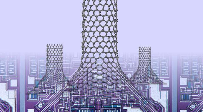
Two-dimensional materials — basically flat sheets that are just one atom in thickness but can be indefinitely large in the other dimensions — have exceptional strength as well as unique electrical properties. But because of their extraordinary thinness, “they are not very useful for making 3-D materials that could be used in vehicles, buildings, or devices,” Buehler says. “What we’ve done is to realize the wish of translating these 2-D materials into three-dimensional structures.”

The team was able to compress small flakes of graphene using a combination of heat and pressure. This process produced a strong, stable structure whose form resembles that of some corals and microscopic creatures called diatoms. These shapes, which have an enormous surface area in proportion to their volume, proved to be remarkably strong. “Once we created these 3-D structures, we wanted to see what’s the limit — what’s the strongest possible material we can produce,” says Qin. To do that, they created a variety of 3-D models and then subjected them to various tests. In computational simulations, which mimic the loading conditions in the tensile and compression tests performed in a tensile loading machine, “one of our samples has 5 percent the density of steel, but 10 times the strength,” Qin says.

Buehler says that what happens to their 3-D graphene material, which is composed of curved surfaces under deformation, resembles what would happen with sheets of paper. Paper has little strength along its length and width, and can be easily crumpled up. But when made into certain shapes, for example rolled into a tube, suddenly the strength along the length of the tube is much greater and can support substantial weight. Similarly, the geometric arrangement of the graphene flakes after treatment naturally forms a very strong configuration.

The new configurations have been made in the lab using a high-resolution, multimaterial 3-D printer. They were mechanically tested for their tensile and compressive properties, and their mechanical response under loading was simulated using the team’s theoretical models. The results from the experiments and simulations matched accurately.

The new, more accurate results, based on atomistic computational modeling by the MIT team, ruled out a possibility proposed previously by other teams: that it might be possible to make 3-D graphene structures so lightweight that they would actually be lighter than air, and could be used as a durable replacement for helium in balloons. The current work shows, however, that at such low densities, the material would not have sufficient strength and would collapse from the surrounding air pressure.

But many other possible applications of the material could eventually be feasible, the researchers say, for uses that require a combination of extreme strength and light weight. “You could either use the real graphene material or use the geometry we discovered with other materials, like polymers or metals,” Buehler says, to gain similar advantages of strength combined with advantages in cost, processing methods, or other material properties (such as transparency or electrical conductivity).

“You can replace the material itself with anything,” Buehler says. “The geometry is the dominant factor. It’s something that has the potential to transfer to many things.”

The unusual geometric shapes that graphene naturally forms under heat and pressure look something like a Nerf ball — round, but full of holes. These shapes, known as gyroids, are so complex that “actually making them using conventional manufacturing methods is probably impossible,” Buehler says. The team used 3-D-printed models of the structure, enlarged to thousands of times their natural size, for testing purposes.

For actual synthesis, the researchers say, one possibility is to use the polymer or metal particles as templates, coat them with graphene by chemical vapor deposit before heat and pressure treatments, and then chemically or physically remove the polymer or metal phases to leave 3-D graphene in the gyroid form. For this, the computational model given in the current study provides a guideline to evaluate the mechanical quality of the synthesis output.

The same geometry could even be applied to large-scale structural materials, they suggest. For example, concrete for a structure such a bridge might be made with this porous geometry, providing comparable strength with a fraction of the weight. This approach would have the additional benefit of providing good insulation because of the large amount of enclosed airspace within it.

Because the shape is riddled with very tiny pore spaces, the material might also find application in some filtration systems, for either water or chemical processing. The mathematical descriptions derived by this group could facilitate the development of a variety of applications, the researchers say.

“This is an inspiring study on the mechanics of 3-D graphene assembly,” says Huajian Gao, a professor of engineering at Brown University, who was not involved in this work. “The combination of computational modeling with 3-D-printing-based experiments used in this paper is a powerful new approach in engineering research. It is impressive to see the scaling laws initially derived from nanoscale simulations resurface in macroscale experiments under the help of 3-D printing,” he says.

This work, Gao says, “shows a promising direction of bringing the strength of 2-D materials and the power of material architecture design together.”

There’s a video describing the work,

Here’s a link to and a citation for the paper,

The mechanics and design of a lightweight three-dimensional graphene assembly by Zhao Qin, Gang Seob Jung, Min Jeong Kang, and Markus J. Buehler. Science Advances  06 Jan 2017: Vol. 3, no. 1, e1601536 DOI: 10.1126/sciadv.1601536  04 January 2017

This paper appears to be open access.

Understanding nanotechnology with Timbits; a peculiarly Canadian explanation

For the uninitiated, Timbits are also known as donut holes. Tim Hortons, founded by ex-National Hockey League player Tim Horton who has since deceased, has taken hold in the Canada’s language and culture such that one of our scientists trying to to explain nanotechnology thought it would be best understood in terms of Timbits. From a Jan. 14, 2017 article (How nanotechnology could change our lives) by Vanessa Lu for thestar.com,

The future is all in the tiny.

Known as nanoparticles, these are the tiniest particles, so small that we can’t see them or even imagine how small they are.

University of Waterloo’s Frank Gu paints a picture of their scale.

“Take a Timbit and start slicing it into smaller and smaller pieces, so small that every Canadian — about 35 million of us — can hold a piece of the treat,” he said. “And those tiny pieces are still a little bigger than a nanoparticle.”

For years, consumers have seen the benefits of nanotechnology in everything from shrinking cellphones to ultrathin televisions. Apple’s iPhones have become more powerful as they have become smaller — where a chip now holds billions of transistors.

“As you go smaller, it creates less footprint and more power,” said Gu, who holds the Canada research chair in advanced targeted delivery systems. “FaceTime, Skype — they are all powered by nanotechnology, with their retina display.”

Lu wrote a second January 14, 2017 article (Researchers developing nanoparticles to purify water) for thestar.com,

When scientists go with their gut or act on a hunch, it can pay off.

For Tim Leshuk, a PhD student in nanotechnology at the University of Waterloo, he knew it was a long shot.

Leshuk had been working with Frank Gu, who leads a nanotechnology research group, on using tiny nanoparticles that have been tweaked with certain properties to purify contaminated water.

Leshuk was working on the process, treating dirty water such as that found in Alberta’s oilsands, with the nanoparticles combined with ultraviolet light. He wondered what might happen if exposed to actual sunlight.

“I didn’t have high hopes,” he said. “For the heck of it, I took some beakers out and put them on the roof. And when I came back, it was far more effective that we had seen with regular UV light.

“It was high-fives all around,” Leshuk said. “It’s not like a Brita filter or a sponge that just soaks up pollutants. It completely breaks them down.”

Things are accelerating quickly, with a spinoff company now formally created called H2nanO, with more ongoing tests scheduled. The research has drawn attention from oilsands companies, and [a] large pre-pilot project to be funded by the Canadian Oil Sands Innovation Alliance is due to get under way soon.

The excitement comes because it’s an entirely green process, converting solar energy for cleanup, and the nanoparticle material is reuseable, over and over.

It’s good to see a couple of articles about nanotechnology. The work by Tim Leshuk was highlighted here in a Dec. 1, 2015 posting titled:  New photocatalytic approach to cleaning wastewater from oil sands. I see the company wasn’t mentioned in the posting so, it must be new; you can find H2nanO here.

Discussion of a divisive topic: the Oilsands

As for the oilsands, it’s been an interesting few days with the Prime Minister’s (Justin Trudeau) suggestion that dependence would be phased out causing a furor of sorts. From a Jan. 13, 2017 article by James Wood for the Calgary Herald,

Prime Minister Justin Trudeau’s musings about phasing out the oilsands Friday [Jan. 13, 2017] were met with a barrage of criticism from Alberta’s conservative politicians and a pledge from Premier Rachel Notley that the province’s energy industry was “not going anywhere, any time soon.”

Asked at a town hall event in Peterborough [Ontario] about the federal government’s recent approval of Kinder Morgan’s Trans Mountain pipeline expansion, Trudeau reiterated his longstanding remarks that he is attempting to balance economic and environmental concerns.

“We can’t shut down the oilsands tomorrow. We need to phase them out. We need to manage the transition off of our dependence on fossil fuels but it’s going to take time and in the meantime we have to manage that transition,” he added.

Northern Alberta’s oilsands are a prime target for environmentalists because of their significant output of greenhouse gas emissions linked to global climate change.

Trudeau, who will be in Calgary for a cabinet retreat on Jan. 23 and 24 [2017], also said again that it is the responsibility of the national government to get Canadian resources to market.

Meanwhile, Jane Fonda, Hollywood actress, weighed in on the issue of the Alberta oilsands with this (from a Jan. 11, 2017 article by Tristan Hopper for the National Post),

Fort McMurrayites might have assumed the celebrity visits would stop after the city was swept first by recession, and then by wildfire.

Or when the provincial government introduced a carbon tax and started phasing out coal.

And surely, with Donald Trump in the White House, even the oiliest corner of Canada would shift to the activist back burner.

But no; here comes Jane Fonda.

“We don’t need new pipelines,” she told a Wednesday [Jan. 11, 2017] press conference at the University of Alberta where she also dismissed Prime Minister Justin Trudeau as a “good-looking Liberal” who couldn’t be trusted.

Saying that her voice was joined with the “Indigenous people of Canada,” Fonda explained her trip to Alberta by saying “when you’re famous you can help amplify the voices of people that can’t necessarily get a lot of press people to come out.”

Fonda is in Alberta at the invitation of Greenpeace, which has brought her here in support of the Treaty Alliance Against Tar Sands Expansion — a group of Canadian First Nations and U.S. tribes opposed to new pipelines to the Athabasca oilsands.

Appearing alongside Fonda, at a table with a sign reading “Respect Indigenous Decisions,” was Grand Chief Stewart Phillip, who, as leader of the Union of B.C. Indian Chiefs, has led anti-pipeline protests and litigation in British Columbia.

“The future is going to be incredibly litigious,” he said in reference to the approved expansion of the Trans-Mountain pipeline.

The event also included Grand Chief Derek Nepinak of the Assembly of Manitoba Chiefs, which is leading a legal challenge to federal approval of the Line 3 pipeline.

Although much of Athabasca’s oil production now comes from “steam-assisted gravity drainage” projects that requires minimal surface disturbance, on Tuesday Fonda took the requisite helicopter tour of a Fort McMurray-area open pit mine.

As you can see, there are not going to be any easy answers.

Sea sponges don’t buckle under pressure

You wouldn’t think a sponge (the sea creature) was particularly tough but it is according to a Jan. 4, 2017 news item on Nanowerk,

Judging by their name alone, orange puffball sea sponges might seem unlikely paragons of structural strength. But maintaining their shape at the bottom of the churning ocean is critical to the creatures’ survival, and new research shows that tiny structural rods in their bodies have evolved the optimal shape to avoid buckling under pressure.

The rods, called strongyloxea spicules, measure about 2 millimeters long and are thinner than a human hair. Hundreds of them are bundled together, forming stiff rib-like structures inside the orange puffball’s spongy body. It was the odd and remarkably consistent shape of each spicule that caught the eye of Brown University engineers Haneesh Kesari and Michael Monn. Each one is symmetrically tapered along its length — going gradually from fatter in the middle to thinner at the ends.

Caption: Tiny rods found inside the bodies of orange puffball sea sponges have an interesting tapered shape. That shape, new research shows, turns out to be a match for the Clausen profile, a column shape shown to be optimal for resistance to buckling failure. Credit: Michael Monn, Haneesh Kesari / Brown University

A Jan. 4, 2017 Brown University news release on EurekAlert, which originated the news item, describes the research in more detail,

Using structural mechanics models and a bit of digging in obscure mathematics journals, Monn and Kesari showed the peculiar shape of the spicules to be optimal for resistance to buckling, the primary mode of failure for slender structures. This natural shape could provide a blueprint for increasing the buckling resistance in all kinds of slender human-made structures, from building columns to bicycle spokes to arterial stents, the researchers say.

“This is one of the rare examples that we’re aware of where a natural structure is not just well-suited for a given function, but actually approaches a theoretical optimum,” said Kesari, an assistant professor of engineering at Brown. “There’s no engineering analog for this shape — we don’t see any columns or other slender structures that are tapered in this way. So in this case, nature has shown us something quite new that we think could be useful in engineering.”

The findings are published in the journal Scientific Reports.

Function and form

Orange puffball sponges (Tethya aurantia) are native to the Mediterranean Sea. They live mainly in rocky coastal environments, where they’re subject to the constant stress of underwater waves and tidal forces. Sponges are filter feeders — they pump water through their bodies to extract nutrients and oxygen. To do this, their bodies need to be porous and compliant, but they also need enough stiffness to avoid being deformed too much.

“If you compress them too much, you’re essentially choking them,” Kesari said. “So maintaining their stiffness is critical to their survival.”

And that means the spicules, which make up the rib-like structures that give sponges their stiffness, are critical components. When Monn and Kesari saw the shapes of the spicules under a microscope, the consistency of the tapered shape from spicule to spicule was hard to miss.

“We saw the shape and wondered if there might be an engineering principle at work here,” Kesari said.

To figure that out, the researchers first needed to understand what forces were acting on each individual spicule. So Monn and Kesari developed a structural mechanics model of spicules bundled within a sponge’s ribs. The model showed that the mismatch in stiffness between the bulk of the sponge’s soft body and the more rigid spicules causes each spicule to experience primarily one type of mechanical loading — a compression load on each of its ends.

“You can imagine taking a toothpick and trying to squeeze it longways between your fingers,” Monn said. “That’s how these spicules see the world.”

The primary mode of failure for a structure with this mechanical load is through buckling. At a certain critical load, the structure starts to bend somewhere along its length. Once the bending starts, the force transferred by the load is amplified at the bending point, which causes the structure to break or collapse.

Once Kesari and Monn knew what forces were acting on the spicules and how they would fail, the next step was looking to see if there was anything special about them that helped them resist buckling. Scanning electron microscope images of the inside of a spicule and other tests showed that they were monolithic silica — essentially glass.

“We could see that there was no funny business going on with the material properties,” Monn said. “If there was anything contributing to its mechanical performance, it would have to be the shape.”

Optimal shape

Kesari and Monn combed the literature to see if they could find anything on tapering in slender structures. They came up empty in the modern engineering literature. But they found something interesting published more than 150 years ago by a German scientist named Thomas Clausen.

In 1851, Clausen proposed that columns that are tapered toward their ends should have more buckling resistance than plain cylinders, which had been and still are the primary design for architectural columns. In the 1960s, mathematician Joseph Keller published an ironclad mathematical proof that the Clausen column was indeed optimal for resistance to buckling — having 33 percent better resistance than a cylinder. Even compared to a very similar shape — an ellipse, which is slightly fatter in the middle and pointier at the ends — the Clausen column had 18 percent better buckling resistance.

Knowing what the optimal column shape is, Monn and Kesari started making precise dimensional measurements of dozens of spicules. They showed that their shapes were remarkably consistent and nearly identical to that of the Clausen column.

“The spicules were a match for the best shape of all possible column shapes,” Monn said.

It seems in this case, natural selection figured out something that engineers have not. Despite the fact that it’s been mathematically shown to be the optimal column shape, the Clausen profile isn’t widely known in the engineering community. Kesari and Monn hope this work might bring it out of the shadows.

“We see this as an addition to our library of structural designs,” Monn said. “We’re not just talking about an improvement of a few percent. This shape is 33 percent better than the cylinder, which is quite an improvement.”

In particular, the shape would be particularly useful in a new generation of materials made from nanoscale truss structures. “It would be easy to 3-D print the Clausen profile into these materials, and you’d get a tremendous increase in buckling resistance, which is often how these materials fail.”

Lessons from nature

The field of bio-inspired engineering began at a time when many people viewed adaptive evolution as an unceasing march toward perfection. If that were true, scientists should find untold numbers of optimal structures in nature.

But the modern understanding of evolution is a bit different. It’s now understood that in order for a trait to be conserved by natural selection, it doesn’t need to be optimal. It just needs to be good enough to work. That has put a bit of a damper on the enthusiasm for bio-inspired engineering, Kesari and Monn say.

However, they say, this work shows that nearly optimal structures are out there if researchers look in the right places. In this case, they looked at creatures from a very old phylum — sea sponges are among the very first animals on Earth — with plenty of time to evolve under consistent selection pressures.

Sponges are also fairly simple creatures, so understanding the function of a given trait is relatively straightforward. In this case, the spicule appears to have one and only one job to do — provide stiffness. Compare that to, for example, human bone, which not only provides support but must also accommodate arteries, provide attachment points for muscles and house bone marrow. Those other functions may cause tradeoffs in adaptations for strength or stiffness.

“With the sponges, you have lots of evolutionary pressure, lots of time and opportunity to respond to that pressure, and functional elements that can be easily identified,” Kesari said.

With those as guiding principles, there may well be more ideal structures out there waiting to be found.

“This work shows that nature can hit an optimum,” Kesari said, “and the biological world can still be hiding completely new designs of considerable technological significance in plain sight.”

Here’s a link to and a citation for the paper,

A new structure-property connection in the skeletal elements of the marine sponge Tethya aurantia that guards against buckling instability by Michael A. Monn & Haneesh Kesari. Scientific Reports 7, Article number: 39547 (2017) doi:10.1038/srep39547 Published online: 04 January 2017

This paper is open access.

Kesari and Monn have researched sea sponges previously as can be seen in my April 7, 2015 posting, which highlights their work on strength and Venus’ flower basket sea sponge.

Nano-chimneys to cut down heat

Heat is always a problem with electronics—even nanoelectronics. Scientists at Rice University (US) believe they may have a solution for nanoelectronics heat problems, according to a Jan. 4, 2017 news item on ScienceDaily,

A few nanoscale adjustments may be all that is required to make graphene-nanotube junctions excel at transferring heat, according to Rice University scientists.

The Rice lab of theoretical physicist Boris Yakobson found that putting a cone-like “chimney” between the graphene and [carbon] nanotube all but eliminates a barrier that blocks heat from escaping.

Caption: Simulations by Rice University scientists show that placing cones between graphene and carbon nanotubes could enhance heat dissipation from nano-electronics. The nano-chimneys become better at conducting heat-carrying phonons by spreading out the number of heptagons required by the graphene-to-nanotube transition. Credit: Alex Kutana/Rice University

A Jan. 4, 2016 Rice University news release (also on EurekAlert), which originated the news item, describes the research in more detail,

Heat is transferred through phonons, quasiparticle waves that also transmit sound. The Rice theory offers a strategy to channel damaging heat away from next-generation nano-electronics.

Both graphene and carbon nanotubes consist of six-atom rings, which create a chicken-wire appearance, and both excel at the rapid transfer of electricity and phonons.

But when a nanotube grows from graphene, atoms facilitate the turn by forming heptagonal (seven-member) rings instead. Scientists have determined that forests of nanotubes grown from graphene are excellent for storing hydrogen for energy applications, but in electronics, the heptagons scatter phonons and hinder the escape of heat through the pillars.

The Rice researchers discovered through computer simulations that removing atoms here and there from the two-dimensional graphene base would force a cone to form between the graphene and the nanotube. The geometric properties (aka topology) of the graphene-to-cone and cone-to-nanotube transitions require the same total number of heptagons, but they are more sparsely spaced and leave a clear path of hexagons available for heat to race up the chimney.

“Our interest in advancing new applications for low-dimensional carbon — fullerenes, nanotubes and graphene — is broad,” Yakobson said. “One way is to use them as building blocks to fill three-dimensional spaces with different designs, creating anisotropic, nonuniform scaffolds with properties that none of the current bulk materials have. In this case, we studied a combination of nanotubes and graphene, connected by cones, motivated by seeing such shapes obtained in our colleagues’ experimental labs.”

The researchers tested phonon conduction through simulations of free-standing nanotubes, pillared graphene and nano-chimneys with a cone radius of either 20 or 40 angstroms. The pillared graphene was 20 percent less conductive than plain nanotubes. The 20-angstrom nano-chimneys were just as conductive as plain nanotubes, while 40-angstrom cones were 20 percent better than the nanotubes.

“The tunability of such structures is virtually limitless, stemming from the vast combinatorial possibilities of arranging the elementary modules,” said Alex Kutana, a Rice research scientist and co-author of the study. “The actual challenge is to find the most useful structures given a vast number of possibilities and then make them in the lab reliably.

“In the present case, the fine-tuning parameters could be cone shapes and radii, nanotube spacing, lengths and diameters. Interestingly, the nano-chimneys also act like thermal diodes, with heat flowing faster in one direction than the other,” he said.

Here’s a link to and a citation for the paper,

Nanochimneys: Topology and Thermal Conductance of 3D Nanotube–Graphene Cone Junctions by Ziang Zhang, Alex Kutana, Ajit Roy, and Boris I. Yakobson. J. Phys. Chem. C, Article ASAP DOI: 10.1021/acs.jpcc.6b11350 Publication Date (Web): December 21, 2016

Copyright © 2016 American Chemical Society

This paper is behind a paywall.

Eliminate cold storage for diagnostic tests?

There’s a nanoparticle coating that could eliminate the need for cold storage and/or refrigeration for diagnostic testing according to a Jan. 4, 2017 news item on Nanowerk,

Many diagnostic tests use antibodies to help confirm a myriad of medical conditions, from Zika infections to heart ailments and even some forms of cancer. Antibodies capture and help detect proteins, enzymes, bacteria and viruses present in injuries and illnesses, and must be kept at a constant low temperature to ensure their viability — often requiring refrigeration powered by electricity. This can make diagnostic testing in underdeveloped countries, disaster or remote areas and even war zones extremely expensive and difficult.

A team of engineers from Washington University in St. Louis and Air Force Research Laboratory have discovered an inexpensive work-around: a protective coating that could completely eliminate the need for cold storage and change the scope of medical diagnostic testing in places where it’s often needed the most.

“In many developing countries, electricity is not guaranteed,” said Srikanth Singamaneni, associate professor of mechanical engineering and materials science in Engineering & Applied Science at Washington University in St. Louis.

“So how do we best get them medical diagnostics? We did not know how to solve this problem previously.”

A Jan. 4, 2016 Washington University in St. Louis news release by Erika Ebsworth-Goold, which originated the news item, describes how previous research helped lead to a solution,

Singamaneni’s team previously used tiny gold nanorods in bio-diagnostic research, measuring changes in their optical properties to quantify protein concentrations in bio-fluids: the higher a concentration, the higher the likelihood of injury or disease.

In this new research, published in Advanced Materials, Singamaneni worked with faculty from Washington University’s School of Medicine and researchers from the Air Force Research Lab to grow metal-organic frameworks (MOFs) around antibodies attached to gold nanorods. The crystalline MOFs formed a protective layer around the antibodies and prevented them from losing activity at elevated temperatures. The protective effect lasted for a week even when the samples were stored at 60°C.

“This technology would allow point-of-care screening for biomarkers of diseases in urban and rural clinic settings where immediate patient follow-up is critical to treatment and wellbeing,” said Dr. Jeremiah J. Morrissey, professor of anesthesiology, Division of Clinical and Translational Research, Washington University School of Medicine and a co-author on the paper.

“On the spot testing eliminates the time lag in sending blood/urine samples to a central lab for testing and in tracking down patients to discuss test results. In addition, it may reduce costs associated with refrigerated shipping and storage.”

The protective MOF layer can be quickly and easily removed from the antibodies with a simple rinse of slightly acidic water, making a diagnostic strip or paper immediately ready to use. Singamaneni says this proof of concept research is now ready to be tested for clinical samples.

“As long as you are using antibodies, you can use this technology,” said Congzhou Wang, a postdoctoral researcher in Singamaneni’s lab and the paper’s lead author. “In bio-diagnostics from here on out, we will no longer need refrigeration.”

“The MOF-based protection of antibodies on sensor surfaces is ideal for preserving biorecognition abilities of sensors that are designed for deployment in the battlefield,” said Dr. Rajesh R. Naik, 711th Human Performance Wing of the Air Force Research Laboratory, Wright-Patterson Air Force Base, and a co-corresponding author of the paper.  “It provides remarkable stability and extremely easy to remove right before use.”

Here’s a link to and a citation for the paper,

Metal-Organic Framework as a Protective Coating for Biodiagnostic Chips by Congzhou Wang, Sirimuvva Tadepalli, Jingyi Luan, Keng-Ku Liu, Jeremiah J. Morrissey, Evan D. Kharasch, Rajesh R. Naik, and Srikanth Singamaneni. Advanced Materials DOI: 10.1002/adma.201604433 Version of Record online: 7 DEC 2016

© 2016 WILEY-VCH Verlag GmbH & Co. KGaA, Weinheim

This paper is behind a paywall.

A final observation, there’s at least one other project aimed at eliminating the need for refrigeration in the field of medical applications and that’s the nanopatch, a replacement for syringes used for liquid medications and vaccines (see my Dec. 16, 2016 posting for a description).

High speed fabrication of adhesive and flexible electronics

For a university that celebrated its opening in Sept. 2009 (mentioned in my Sept. 24, 2009 posting; scroll down about 40% of the way; look for a reference to the House of Wisdom), the King Abdullah University of Science and Technology (KAUST) has made some impressive announcements including this one in a Jan. 3, 2017 press release on EurekAlert,

The healthcare industry forecasts that our wellbeing in the future will be monitored by wearable wirelessly networked sensors. Manufacturing such devices could become much easier with decal electronics. A KAUST-developed process prints these high-performance silicon-based computers on to soft, sticker-like surfaces that can be attached anywhere1.

Fitting electronics on to the asymmetric contours of human bodies demands a re-think of traditional computer fabrications. One approach is to print circuit patterns on to materials such as polymers or cellulose using liquid ink made from conductive molecules. This technique enables high-speed roll-to-roll assembly of devices and packaging at low costs.

Flexible printed circuits, however, require conventional silicon components to handle applications such as digitizing analog signals. Such rigid modules can create uncomfortable hot spots on the body and increase device weight.

For the past four years, Muhammad Hussain and his team from the KAUST Computer, Electrical and Mathematical Science and Engineering Division have investigated ways to improve the flexibility of silicon materials while retaining their performance.

“We are trying to integrate all device components–sensors, data management electronics, battery, antenna–into a completely compliant system,” explained Hussain. “However, packaging these discrete modules on to soft substrates is extremely difficult.”

Searching for potential electronic skin applications, the researchers developed a sensor containing narrow strips of aluminum foil that changes conductivity at different bending states.

The devices, which could monitor a patient’s breathing patterns or activity levels, feature high-mobility zinc oxide nanotransistors on silicon wafers thinned down lithographically to microscale dimensions for maximum flexibility. Using three-dimensional (3-D) printing techniques, the team encapsulated the silicon chips and foils into a polymer film backed by an adhesive layer.

Hussain and his colleagues found a way to make the e-sticker sensors work in multiple applications. They used inkjet printing to write conductive wiring patterns on to different surfaces, such as paper or clothing. Custom-printed decals were then attached or re-adhered to each location.

“You can place a pressure-sensing decal on a tire to monitor it while driving and then peel it off and place it on your mattress to learn your sleeping patterns,” said Galo Torres Sevilla, first author of the findings and a KAUST Ph.D. graduate.

The robust performance and high-throughput manufacturing potential of decal electronics could launch a number of innovative sensor deployments, noted Hussain.

“I believe that electronics have to be democratized–simple to learn and easy to implement. Electronic decals are a right step in that direction,” Hussain said.

Here’s a link to and a citation for the paper,

Decal Electronics: Printable Packaged with 3D Printing High-Performance Flexible CMOS Electronic Systems by Galo A. Torres Sevilla, Marlon D. Cordero, Joanna M. Nassar, Amir N. Hanna, Arwa T. Kutbee, Arpys Arevalo, and Muhammad M. Hussain. Advanced Materials Technologies DOI: 10.1002/admt.201600175 Version of Record online: 13 OCT 2016

© 2016 WILEY-VCH Verlag GmbH & Co. KGaA, Weinheim

This paper is behind a paywall.

Are there any leaders in the ‘graphene race’?

Tom Eldridge, a director and co-founder of Fullerex, has written a Jan. 5, 2017 essay titled: Is China still leading the graphene race? for Nanotechnology Now. Before getting to the essay, here’s a bit more about Fullerex and Tom Eldridge’s qualifications. From Fullerex’s LinkedIn description,

Fullerex is a leading independent broker of nanomaterials and nano-intermediates. Our mission is to support the advancement of nanotechnology in creating radical, transformative and sustainable improvement to society. We are dedicated to achieving these aims by accelerating the commercialisation and usage of nanomaterials across industry and beyond. Fullerex is active in market development and physical trading of advanced materials. We generate demand for nanomaterials across synergistic markets by stimulating innovation with end-users and ensuring robust supply chains are in place to address the growing commercial trade interest. Our end-user markets include Polymers and Polymer Composites, Coatings, Tyre and Rubber, Cementitious Composites, 3D Printing and Printed Electronics, the Energy sector, Lubricating Oils and Functional Fluids. The materials we cover: Nanomaterials: Includes fullerenes, carbon nanotubes and graphene, metal and metal oxide nanoparticles, and organic-inorganic hybrids. Supplied as raw nanopowders or ready-to-use dispersions and concentrates. Nano-intermediates: Producer goods and semi-finished products such as nano-enabled coatings, polymer masterbatches, conductive inks, thermal interface materials and catalysts.

As for Tom Eldridge, here’s more about him, his brother, and the company from the Fullerex About page,

Fullerex was founded by Joe and Tom Eldridge, brothers with a keen interest in nanotechnology and the associated emerging market for nanomaterials.

Joe has a strong background in trading with nearly 10 years’ experience as a stockbroker, managing client accounts for European Equities and FX. At University he read Mathematics at Imperial College London gaining a BSc degree and has closely followed the markets for disruptive technologies and advanced materials for a number of years.

Tom worked in the City of London for 7 years in commercial roles throughout his professional career, with an expertise in market data, financial and regulatory news. In his academic background, he earned a BSc degree in Physics and Philosophy at Kings College London and is a member of the Institute of Physics.

As a result, Fullerex has the strong management composition that allows the company to support the growth of the nascent and highly promising nanomaterials industry. Fullerex is a flexible company with drive, enthusiasm and experience, committed to aiding the development of this market.

Getting back to the matter at hand, that’s a rather provocative title for Tom Eldridge’s essay,. given that he’s a Brit and (I believe) the Brits viewed themselves as leaders in the ‘graphene race’ but he offers a more nuanced analysis than might be expected from the title. First, the patent landscape (from Eldridge’s Jan. 5, 2017 essay),

As competition to exploit the “wonder material” has intensified around the world, detailed reports have so far been published which set out an in-depth depiction of the global patent landscape for graphene, notably from CambridgeIP and the UK Intellectual Property Office, in 2013 and 2015 respectively. Ostensibly the number of patents and patent applications both indicated that China was leading the innovation in graphene technology. However, on closer inspection it became less clear as to how closely the patent figures themselves reflect actual progress and whether this will translate into real economic impact. Some of the main reasons to be doubtful included:

– 98% of the Chinese patent applications only cover China, so therefore have no worldwide monopoly.
– A large number of the Chinese patents are filed in December, possibly due to demand to meet patent quotas. The implication being that the patent filings follow a politically driven agenda, rather than a purely innovation or commercially driven agenda.
– In general, inventors could be more likely to file for patent protection in some countries rather than others e.g. for tax purposes. Which therefore does not give a truly accurate picture of where all the actual research activity is based.
– Measuring the proportion of graphene related patents to overall patents is more indicative of graphene specialisation, which shows that Singapore has the largest proportion of graphene patents, followed by China, then South Korea.

(Intellectual Property Office, 2015), (Ellis, 2015), (CambridgeIP, 2013)

Then, there’s the question of production,

Following the recent launch of the latest edition of the Bulk Graphene Pricing Report, which is available exclusively through The Graphene Council, Fullerex has updated its comprehensive list of graphene producers worldwide, and below is a summary of the number of graphene producers by country in 2017.

Summary Table Showing the Number of Graphene Producers by Country and Region

The total number of graphene producers identified is 142, across 27 countries. This research expands upon previous surveys of the graphene industry, such as the big data analysis performed by Nesta in 2015 (Shapira, 2015). The study by Nesta [formerly  NESTA, National Endowment for Science, Technology and the Arts) is an independent charity that works to increase the innovation capacity of the UK; see Wikipedia here for more about NESTA] revealed 65 producers throughout 16 countries but was unable to glean accurate data on producers in Asia, particularly China.

As we can now see however from the data collected by Fullerex, China has the largest number of graphene producers, followed by the USA, and then the UK.

In addition to having more companies active in the production and sale of graphene than any other country, China also holds about 2/3rds of the global production capacity, according to Fullerex.

Eldridge goes on to note that the ‘graphene industry’ won’t truly grow and develop until there are substantive applications for the material. He also suggests taking another look at the production figures,

As with the patent landscape, rather than looking at the absolute figures, we can review the numbers in relative terms. For instance, if we normalise to account for the differences in the size of each country, by looking at the number of producers as a proportion of GDP, we see the following: Spain (7.18), UK (4.48), India (3.73), China (3.57), Canada (3.28) [emphasis mine], USA (1.79) (United Nations, 2013).

Unsurprisingly, each leading country has a national strategy for economic development which involves graphene prominently.

For instance, The Spanish Council for Scientific Research has lent 9 of its institutes along with 10 universities and other public R&D labs involved in coordinating graphene projects with industry.

The Natural Sciences and Engineering Research Council of Canada [NSERC] has placed graphene as one of five research topics in its target area of “Advanced Manufacturing” for Strategic Partnership Grants.

The UK government highlights advanced materials as one of its Eight Great Technologies, within which graphene is a major part of, having received investment for the NGI and GEIC buildings, along with EPSRC and Innovate UK projects. I wrote previously about the UK punching above its weight in terms of research, ( http://fullerex.com/index.php/articles/130-the-uk-needs-an-industrial-revolution-can-graphene-deliver/ ) but that R&D spending relative to GDP was too low compared to other developed nations. It is good to see that investment into graphene production in the UK is bucking that trend, and we should anticipate this will provide a positive economic outcome.

Yes, I’m  particularly interested in the fact Canada becomes more important as a producer when the numbers are relative but it is interesting to compare the chart with Eldridge’s text and to note how importance shifts depending on what numbers are being considered.

I recommend reading Eldridge’s piece in its entirety.

A few notes about graphene in Canada

By the way, the information in Eldridge’s essay about NSERC’s placement of graphene as a target area for grants is news to me. (As I have often noted here, I get more information about the Canadian nano scene from international sources than I do from our national sources.)

Happily I do get some home news such as a Jan. 5, 2017 email update from Lomiko Metals, a Canadian junior exploration company focused on graphite and lithium. The email provides the latest information from the company (as I’m not an expert in business or mining this is not an endorsement),

On December 13, 2016 we were excited to announce the completion of our drill program at the La Loutre flake graphite property. We received very positive results from our 1550 meter drilling program in 2015 in the area we are drilling now. In that release I stated, “”The intercepts of multiple zones of mineralization in the Refractory Zone where we have reported high grade intercepts previously is a very promising sign. The samples have been rushed to the ALS Laboratory for full assay testing,” We hope to have the results of those assays shortly.

December 16, 2016 Lomiko announced a 10:1 roll back of our shares. We believe that this roll back is important as we work towards securing long term equity financing for the company. Lomiko began trading on the basis of the roll back on December 19.

We believe that Graphite has a bright future because of the many new products that will rely on the material. I have attached a link to a video on Lomiko, Graphite and Graphene.  

https://youtu.be/Y–Y_Ub6oC4

January 3, 2017 Lomiko announced the extension and modification of its option agreements with Canadian Strategic Metals Inc. for the La Loutre and Lac des Iles properties. The effect of this extension is to give Lomiko additional time to complete the required work under the agreements.

Going forward Lomiko is in a much stronger position as the result of our share roll back. Potential equity funders who are very interested in our forthcoming assay results from La Loutre and the overall prospects of the company, have been reassured by our share consolidation.

Looking forward to 2017, we anticipate the assays of the La Loutre drilling to be delivered in the next 90 days, sooner we hope. We also anticipate additional equity funding will become available for the further exploration and delineation of the La Loutre and Lac des Iles properties and deposits.

More generally, we are confident that the market for large flake graphite will become firmer in 2017. Lomiko’s strategy of identifying near surface, ready to mine, graphite nodes puts us in the position to take advantage of improvements in the graphite price without having to commit large sums to massive mine development. As we identify and analyze the graphite nodes we are finding we increase the potential resources of the company. 2017 should see significantly improved resource estimates for Lomiko’s properties.

As I wasn’t familiar with the term ‘roll back of shares’, I looked it up and found this in an April 18, 2012 posting by Dudley Pierce Baker on kitco.com,

As a general rule, we hate to see an announcement of a share rollback, however, there exceptions which we cover below. Investors should always be aware that if a company has, say over 150 million shares outstanding, in our opinion, it is a potential candidate for a rollback and the announcement should not come as a surprise.

Weak markets, a low share price, a large number of shares outstanding, little or no cash and you have a company which is an idea candidate for a rollback.

The basic concept of a rollback or consolidation in a company’s shares is rather simple.

We are witnessing a few cases of rollbacks not with the purpose of raising more money but rather to facilitate the listing of the company’s shares on the NYSE [New York Stock Exchange] Amex.

I have no idea what situation Lomiko finds itself in but it should be noted that graphere research has been active since 2004 when the first graphene sheets were extracted from graphite. This is a relatively new field of endeavour and Lomiko (along with other companies) is in the position of pioneering the effort here in Canada. That said, there are many competitors to graphene and major international race to commercialize nanotechnology-enabled products.

Are there any leaders in the ‘graphene race?

Getting back to the question in the headline, I don’t think there are any leaders at the moment. No one seems to have what they used to call “a killer app,” that one application/product that everyone wants and which drive demand for graphene.

The mathematics of Disney’s ‘Moana’

The hit Disney movie “Moana” features stunning visual effects, including the animation of water to such a degree that it becomes a distinct character in the film. Courtesy of Walt Disney Animation Studios

Few people think to marvel over the mathematics when watching an animated feature but without mathematicians, the artists would not be able to achieve their artistic goals as a Jan. 4, 2017 news item on phys.org makes clear (Note: A link has been removed),

UCLA [University of California at Los Angeles] mathematics professor Joseph Teran, a Walt Disney consultant on animated movies since 2007, is under no illusion that artists want lengthy mathematics lessons, but many of them realize that the success of animated movies often depends on advanced mathematics.

“In general, the animators and artists at the studios want as little to do with mathematics and physics as possible, but the demands for realism in animated movies are so high,” Teran said. “Things are going to look fake if you don’t at least start with the correct physics and mathematics for many materials, such as water and snow. If the physics and mathematics are not simulated accurately, it will be very glaring that something is wrong with the animation of the material.”

Teran and his research team have helped infuse realism into several Disney movies, including “Frozen,” where they used science to animate snow scenes. Most recently, they applied their knowledge of math, physics and computer science to enliven the new 3-D computer-animated hit, “Moana,” a tale about an adventurous teenage girl who is drawn to the ocean and is inspired to leave the safety of her island on a daring journey to save her people.

A Jan. 3, 2017 UCLA news release, which originated the news item, explains in further nontechnical detail,

Alexey Stomakhin, a former UCLA doctoral student of Teran’s and Andrea Bertozzi’s, played an important role in the making of “Moana.” After earning his Ph.D. in applied mathematics in 2013, he became a senior software engineer at Walt Disney Animation Studios. Working with Disney’s effects artists, technical directors and software developers, Stomakhin led the development of the code that was used to simulate the movement of water in “Moana,” enabling it to play a role as one of the characters in the film.

“The increased demand for realism and complexity in animated movies makes it preferable to get assistance from computers; this means we have to simulate the movement of the ocean surface and how the water splashes, for example, to make it look believable,” Stomakhin explained. “There is a lot of mathematics, physics and computer science under the hood. That’s what we do.”

“Moana” has been praised for its stunning visual effects in words the mathematicians love hearing. “Everything in the movie looks almost real, so the movement of the water has to look real too, and it does,” Teran said. “’Moana’ has the best water effects I’ve ever seen, by far.”

Stomakhin said his job is fun and “super-interesting, especially when we cheat physics and step beyond physics. It’s almost like building your own universe with your own laws of physics and trying to simulate that universe.

“Disney movies are about magic, so magical things happen which do not exist in the real world,” said the software engineer. “It’s our job to add some extra forces and other tricks to help create those effects. If you have an understanding of how the real physical laws work, you can push parameters beyond physical limits and change equations slightly; we can predict the consequences of that.”

To make animated movies these days, movie studios need to solve, or nearly solve, partial differential equations. Stomakhin, Teran and their colleagues build the code that solves the partial differential equations. More accurately, they write algorithms that closely approximate the partial differential equations because they cannot be solved perfectly. “We try to come up with new algorithms that have the highest-quality metrics in all possible categories, including preserving angular momentum perfectly and preserving energy perfectly. Many algorithms don’t have these properties,” Teran said.

Stomakhin was also involved in creating the ocean’s crashing waves that have to break at a certain place and time. That task required him to get creative with physics and use other tricks. “You don’t allow physics to completely guide it,” he said.  “You allow the wave to break only when it needs to break.”

Depicting boats on waves posed additional challenges for the scientists.

“It’s easy to simulate a boat traveling through a static lake, but a boat on waves is much more challenging to simulate,” Stomakhin said. “We simulated the fluid around the boat; the challenge was to blend that fluid with the rest of the ocean. It can’t look like the boat is splashing in a little swimming pool — the blend needs to be seamless.”

Stomakhin spent more than a year developing the code and understanding the physics that allowed him to achieve this effect.

“It’s nice to see the great visual effect, something you couldn’t have achieved if you hadn’t designed the algorithm to solve physics accurately,” said Teran, who has taught an undergraduate course on scientific computing for the visual-effects industry.

While Teran loves spectacular visual effects, he said the research has many other scientific applications as well. It could be used to simulate plasmas, simulate 3-D printing or for surgical simulation, for example. Teran is using a related algorithm to build virtual livers to substitute for the animal livers that surgeons train on. He is also using the algorithm to study traumatic leg injuries.

Teran describes the work with Disney as “bread-and-butter, high-performance computing for simulating materials, as mechanical engineers and physicists at national laboratories would. Simulating water for a movie is not so different, but there are, of course, small tweaks to make the water visually compelling. We don’t have a separate branch of research for computer graphics. We create new algorithms that work for simulating wide ranges of materials.”

Teran, Stomakhin and three other applied mathematicians — Chenfanfu Jiang, Craig Schroeder and Andrew Selle — also developed a state-of-the-art simulation method for fluids in graphics, called APIC, based on months of calculations. It allows for better realism and stunning visual results. Jiang is a UCLA postdoctoral scholar in Teran’s laboratory, who won a 2015 UCLA best dissertation prize.  Schroeder is a former UCLA postdoctoral scholar who worked with Teran and is now at UC Riverside. Selle, who worked at Walt Disney Animation Studios, is now at Google.

Their newest version of APIC has been accepted for publication by the peer-reviewed Journal of Computational Physics.

“Alexey is using ideas from high-performance computing to make movies,” Teran said, “and we are contributing to the scientific community by improving the algorithm.”

Unfortunately, the paper does not seem to have been published early online so I cannot offer a link.

Final comment, it would have been interesting to have had a comment from one of the film’s artists or animators included in the article but it may not have been possible due to time or space constraints.

‘Brewing up’ conductive inks for printable electronics

Scientists from Duke University aren’t exactly ‘brewing’ or ‘cooking up’ the inks but they do come close according to a Jan. 3, 2017 news item on ScienceDaily,

By suspending tiny metal nanoparticles in liquids, Duke University scientists are brewing up conductive ink-jet printer “inks” to print inexpensive, customizable circuit patterns on just about any surface.

A Jan. 3, 2017 Duke University news release (also on EurekAlert), which originated the news item, explains why this technique could lead to more accessible printed electronics,

Printed electronics, which are already being used on a wide scale in devices such as the anti-theft radio frequency identification (RFID) tags you might find on the back of new DVDs, currently have one major drawback: for the circuits to work, they first have to be heated to melt all the nanoparticles together into a single conductive wire, making it impossible to print circuits on inexpensive plastics or paper.

A new study by Duke researchers shows that tweaking the shape of the nanoparticles in the ink might just eliminate the need for heat.

By comparing the conductivity of films made from different shapes of silver nanostructures, the researchers found that electrons zip through films made of silver nanowires much easier than films made from other shapes, like nanospheres or microflakes. In fact, electrons flowed so easily through the nanowire films that they could function in printed circuits without the need to melt them all together.

“The nanowires had a 4,000 times higher conductivity than the more commonly used silver nanoparticles that you would find in printed antennas for RFID tags,” said Benjamin Wiley, assistant professor of chemistry at Duke. “So if you use nanowires, then you don’t have to heat the printed circuits up to such high temperature and you can use cheaper plastics or paper.”

“There is really nothing else I can think of besides these silver nanowires that you can just print and it’s simply conductive, without any post-processing,” Wiley added.

These types of printed electronics could have applications far beyond smart packaging; researchers envision using the technology to make solar cells, printed displays, LEDS, touchscreens, amplifiers, batteries and even some implantable bio-electronic devices. The results appeared online Dec. 16 [2016] in ACS Applied Materials and Interfaces.

Silver has become a go-to material for making printed electronics, Wiley said, and a number of studies have recently appeared measuring the conductivity of films with different shapes of silver nanostructures. However, experimental variations make direct comparisons between the shapes difficult, and few reports have linked the conductivity of the films to the total mass of silver used, an important factor when working with a costly material.

“We wanted to eliminate any extra materials from the inks and simply hone in on the amount of silver in the films and the contacts between the nanostructures as the only source of variability,” said Ian Stewart, a recent graduate student in Wiley’s lab and first author on the ACS paper.

Stewart used known recipes to cook up silver nanostructures with different shapes, including nanoparticles, microflakes, and short and long nanowires, and mixed these nanostructures with distilled water to make simple “inks.” He then invented a quick and easy way to make thin films using equipment available in just about any lab — glass slides and double-sided tape.

“We used a hole punch to cut out wells from double-sided tape and stuck these to glass slides,” Stewart said. By adding a precise volume of ink into each tape “well” and then heating the wells — either to relatively low temperature to simply evaporate the water or to higher temperatures to begin melting the structures together — he created a variety of films to test.

The team say they weren’t surprised that the long nanowire films had the highest conductivity. Electrons usually flow easily through individual nanostructures but get stuck when they have to jump from one structure to the next, Wiley explained, and long nanowires greatly reduce the number of times the electrons have to make this “jump”.

But they were surprised at just how drastic the change was. “The resistivity of the long silver nanowire films is several orders of magnitude lower than silver nanoparticles and only 10 times greater than pure silver,” Stewart said.

The team is now experimenting with using aerosol jets to print silver nanowire inks in usable circuits. Wiley says they also want to explore whether silver-coated copper nanowires, which are significantly cheaper to produce than pure silver nanowires, will give the same effect.

Here’s a link to and a citation for the paper,

Effect of Morphology on the Electrical Resistivity of Silver Nanostructure Films by Ian E. Stewart, Myung Jun Kim, and Benjamin J. Wiley. ACS Appl. Mater. Interfaces, Article ASAP
DOI: 10.1021/acsami.6b12289 Publication Date (Web): December 16, 2016

Copyright © 2016 American Chemical Society

This paper is behind a paywall but there is an image of the silver nanowires, which is not exactly compensation but is interesting,

Caption: Duke University chemists have found that silver nanowire films like these conduct electricity well enough to form functioning circuits without applying high temperatures, enabling printable electronics on heat-sensitive materials like paper or plastic.
Credit: Ian Stewart and Benjamin Wiley

A plasmonic nanolaser operating at visible light frequencies using ‘dark lattice’ modes

Finnish scientists have created lasers made of nanoparticles according to a Jan. 3, 2017 news item on ScienceDaily,

Researchers at Aalto University, Finland are the first to develop a plasmonic nanolaser that operates at visible light frequencies and uses so-called dark lattice modes.

The laser works at length scales 1000 times smaller than the thickness of a human hair. The lifetimes of light captured in such small dimensions are so short that the light wave has time to wiggle up and down only a few tens or hundreds of times. The results open new prospects for on-chip coherent light sources, such as lasers, that are extremely small and ultrafast.

The laser operation in this work is based on silver nanoparticles arranged in a periodic array.

A Jan. 3, 2017 Aalto University press release (also on EurekAlert), which originated the news item, describes the work in more detail,

 In contrast to conventional lasers, where the feedback of the lasing signal is provided by ordinary mirrors, this nanolaser utilizes radiative coupling between silver nanoparticles. These 100-nanometer-sized particles act as tiny antennas. To produce high intensity laser light, the interparticle distance was matched with the lasing wavelength so that all particles of the array radiate in unison. Organic fluorescent molecules were used to provide the input energy (the gain) that is needed for lasing.

Light from the dark

A major challenge in achieving lasing this way was that light may not exist long enough in such small dimensions to be helpful. The researchers found a smart way around this potential problem: they produced lasing in dark modes.

“A dark mode can be intuitively understood by considering regular antennas: A single antenna, when driven by a current, radiates strongly, whereas two antennas — if driven by opposite currents and positioned very close to each other — radiate very little,” explains Academy Professor Päivi Törmä.

“A dark mode in a nanoparticle array induces similar opposite-phase currents in each nanoparticle, but now with visible light frequencies”, she continues.

“Dark modes are attractive for applications where low power consumption is needed. But without any tricks, dark mode lasing would be quite useless because the light is essentially trapped at the nanoparticle array and cannot leave”, adds staff scientist Tommi Hakala.

“But by utilizing the small size of the array, we found an escape route for the light. Towards the edges of the array, the nanoparticles start to behave more and more like regular antennas that radiate to the outer world”, tells Ph.D. student Heikki Rekola.

The research team used the nanofabrication facilities and cleanrooms of the national OtaNano research infrastructure.

The researchers have produced a video elucidating their research,

A revelatory soundtrack by Kevin MacLeod has been added to this video.

Finally, here’s a link to and a citation for the paper,

Lasing in dark and bright modes of a finite-sized plasmonic lattice by T. K. Hakala, H. T. Rekola, A. I. Väkeväinen, J.-P. Martikainen, M. Nečada, A. J. Moilanen & P. Törmä. Nature Communications  8, Article number: 13687 doi:10.1038/ncomms13687 Published 03 January 2017

This is an open access paper.