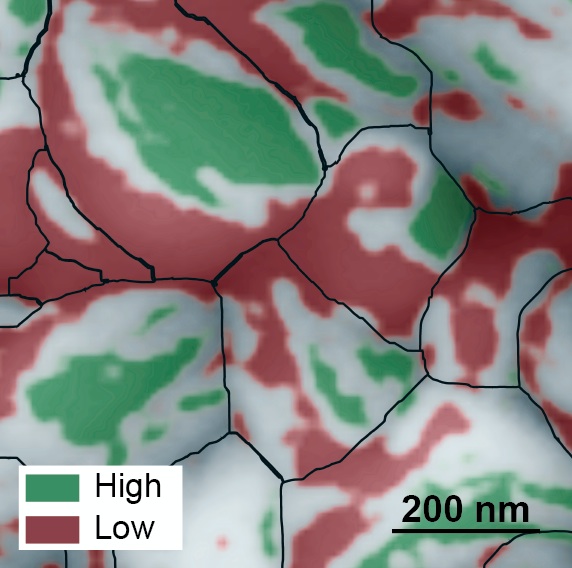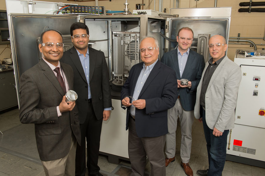
Argonne researchers, from left, Subramanian Sankaranarayanan, Badri Narayanan, Ali Erdemir, Giovanni Ramirez and Osman Levent Eryilmaz show off metal engine parts that have been treated with a diamond-like carbon coating similar to one developed and explored by the team. The catalytic coating interacts with engine oil to create a self-healing diamond-like film that could have profound implications for the efficiency and durability of future engines. (photo by Wes Agresta)
An Aug. 5, 2016 news item on ScienceDaily makes the announcement,
Fans of Superman surely recall how the Man of Steel used immense heat and pressure generated by his bare hands to form a diamond out of a lump of coal.
The tribologists — scientists who study friction, wear, and lubrication — and computational materials scientists at the U.S. Department of Energy’s (DOE’s) Argonne National Laboratory will probably never be mistaken for superheroes. However, they recently applied the same principles and discovered a revolutionary diamond-like film of their own that is generated by the heat and pressure of an automotive engine.
An Aug. 5, 2016 Argonne National Laboratory news release (also on EurekAlert) by Greg Cunningham, which originated the news item, explains further,
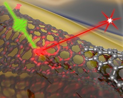
The discovery of this ultra-durable, self-lubricating tribofilm – a film that forms between moving surfaces — was first reported yesterday in the journal Nature. It could have profound implications for the efficiency and durability of future engines and other moving metal parts that can be made to develop self-healing, diamond-like carbon (DLC) tribofilms.
“This is a very unique discovery, and one that was a little unexpected,” said Ali Erdemir, the Argonne Distinguished Fellow who leads the team. “We have developed many types of diamond-like carbon coatings of our own, but we’ve never found one that generates itself by breaking down the molecules of the lubricating oil and can actually regenerate the tribofilm as it is worn away.”
The phenomenon was first discovered several years ago by Erdemir and his colleague Osman Levent Eryilmaz in the Tribology and Thermal-Mechanics Department in Argonne’s Center for Transportation Research. But it took theoretical insight enhanced by the massive computing resources available at Argonne to fully understand what was happening at the molecular level in the experiments. The theoretical understanding was provided by lead theoretical researcher Subramanian Sankaranarayanan and postdoctoral researcher Badri Narayanan from the Center for Nanoscale Materials (CNM), while the computing power was provided by the Argonne Leadership Computing Facility (ALCF) and the National Energy Research Scientific Computing Center (NERSC) at Lawrence Berkeley National Laboratory. CNM, ALCF and NERSC are all DOE Office of Science User Facilities.
The original discovery occurred when Erdemir and Eryilmaz decided to see what would happen when a small steel ring was coated with a catalytically active nanocoating – tiny molecules of metals that promote chemical reactions to break down other materials – then subjected to high pressure and heat using a base oil without the complex additives of modern lubricants. When they looked at the ring after the endurance test, they didn’t see the expected rust and surface damage, but an intact ring with an odd blackish deposit on the contact area.
“This test creates extreme contact pressure and temperatures, which are supposed to cause the ring to wear and eventually seize,” said Eryilmaz. “But this ring didn’t significantly wear and this blackish deposit was visible. We said, ‘This material is strange. Maybe this is what is causing this unusual effect.'”
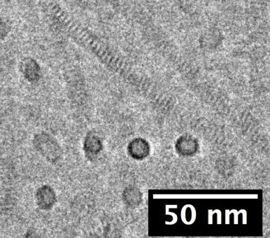
Looking at the deposit using high-powered optical and laser Raman microscopes, the experimentalists realized the deposit was a tribofilm of diamond-like carbon, similar to several other DLCs developed at Argonne in the past. But it worked even better. Tests revealed the DLC tribofilm reduced friction by 25 to 40 percent and that wear was reduced to unmeasurable values.
Further experiments, led by postdoctoral researcher Giovanni Ramirez, revealed that multiple types of catalytic coatings can yield DLC tribofilms. The experiments showed the coatings interact with the oil molecules to create the DLC film, which adheres to the metal surfaces. When the tribofilm is worn away, the catalyst in the coating is re-exposed to the oil, causing the catalysis to restart and develop new layers of tribofilm. The process is self-regulating, keeping the film at consistent thickness. The scientists realized the film was developing spontaneously between the sliding surfaces and was replenishing itself, but they needed to understand why and how.
To provide the theoretical understanding of what the tribology team was seeing in its experiments, they turned to Sankaranarayanan and Narayanan, who used the immense computing power of ALCF’s 10-petaflop supercomputer, Mira. They ran large-scale simulations to understand what was happening at the atomic level, and determined that the catalyst metals in the nanocomposite coatings were stripping hydrogen atoms from the hydrocarbon chains of the lubricating oil, then breaking the chains down into smaller segments. The smaller chains joined together under pressure to create the highly durable DLC tribofilm.
“This is an example of catalysis under extreme conditions created by friction. It is opening up a new field where you are merging catalysis and tribology, which has never been done before,” said Sankaranarayanan. “This new field of tribocatalysis has the potential to change the way we look at lubrication.”
The theorists explored the origins of the catalytic activity to understand how catalysis operates under the extreme heat and pressure in an engine. By gaining this understanding, they were able to predict which catalysts would work, and which would create the most advantageous tribofilms.
“Interestingly, we found several metals or composites that we didn’t think would be catalytically active, but under these circumstances, they performed quite well,” said Narayanan. “This opens up new pathways for scientists to use extreme conditions to enhance catalytic activity.”
The implications of the new tribofilm for efficiency and reliability of engines are huge. Manufacturers already use many different types of coatings — some developed at Argonne — for metal parts in engines and other applications. The problem is those coatings are expensive and difficult to apply, and once they are in use, they only last until the coating wears through. The new catalyst allows the tribofilm to be continually renewed during operation.
Additionally, because the tribofilm develops in the presence of base oil, it could allow manufacturers to reduce, or possibly eliminate, some of the modern anti-friction and anti-wear additives in oil. These additives can decrease the efficiency of vehicle catalytic converters and can be harmful to the environment because of their heavy metal content.
Here’s a link to and a citation for the paper,
Carbon-based tribofilms from lubricating oils by Ali Erdemir, Giovanni Ramirez, Osman L. Eryilmaz, Badri Narayanan, Yifeng Liao, Ganesh Kamath, & Subramanian K. R. S. Sankaranarayanan. Nature 536, 67–71 (04 August 2016) doi:10.1038/nature18948 Published online 03 August 2016
This paper is behind a paywall.