Tag Archives: Konstantin Novoselov

Should October 2013 be called ‘the month of graphene’?

Since the Oct. 10-11, 2013 Graphene Flagship (1B Euros investment) launch, mentioned in my preview Oct. 7, 2013 posting, there’ve been a flurry of graphene-themed news items both on this blog and elsewhere and I’ve decided to offer a brief roundup what I’ve found elsewhere.

Dexter Johnson offers a commentary in the pithily titled, Europe Invests €1 Billion to Become “Graphene Valley,” an Oct. 15, 2013 posting on his Nanoclast blog (on the IEEE [Institute of Electrical and Electronics Engineers] website) Note: Links have been removed,

The initiative has been dubbed “The Graphene Flagship,” and apparently it is the first in a number of €1 billion, 10-year plans the EC is planning to launch. The graphene version will bring together 76 academic institutions and industrial groups from 17 European countries, with an initial 30-month-budget of €54M ($73 million).

Graphene research is still struggling to find any kind of applications that will really take hold, and many don’t expect it will have a commercial impact until 2020. What’s more, manufacturing methods are still undeveloped. So it would appear that a 10-year plan is aimed at the academic institutions that form the backbone of this initiative rather than commercial enterprises.

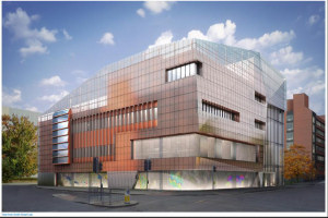
Just from a political standpoint the choice of Chalmers University in Sweden as the base of operations for the Graphene Flagship is an intriguing choice. …

I have to agree with Dexter that choosing Chalmers University over the University of Manchester where graphene was first isolated is unexpected. As a companion piece to reading Dexter’s posting in its entirety and which features a video from the flagship launch, you might want to try this Oct. 15, 2013 article by Koen Mortelmans for Youris (h/t Oct. 15, 2013 news item on Nanowerk),

Andre Konstantin Geim is the only person who ever received both a Nobel and an Ig Nobel. He was born in 1958 in Russia, and is a Dutch-British physicist with German, Polish, Jewish and Ukrainian roots. “Having lived and worked in several European countries, I consider myself European. I don’t believe that any further taxonomy is necessary,” he says. He is now a physics professor at the University of Manchester. …

He shared the Noble [Nobel] Prize in 2010 with Konstantin Novoselov for their work on graphene. It was following on their isolation of microscope visible grapheme flakes that the worldwide research towards practical applications of graphene took off.  “We did not invent graphene,” Geim says, “we only saw what was laid up for five hundred year under our noses.”

Geim and Novoselov are often thought to have succeeded in separating graphene from graphite by peeling it off with ordinary duct tape until there only remained a layer. Graphene could then be observed with a microscope, because of the partial transparency of the material. That is, after dissolving the duct tape material in acetone, of course. That is also the story Geim himself likes to tell.

However, he did not use – as the urban myth goes – graphite from a common pencil. Instead, he used a carbon sample of extreme purity, specially imported. He also used ultrasound techniques. But, probably the urban legend will survive, as did Archimedes’ bath and Newtons apple. “It is nice to keep some of the magic,” is the expression Geim often uses when he does not want a nice story to be drowned in hard facts or when he wants to remain discrete about still incomplete, but promising research results.

Mortelmans’ article fills in some gaps for those not familiar with the graphene ‘origins’ story while Tim Harper’s July 22, 2012 posting on Cientifica’s (an emerging technologies consultancy where Harper is the CEO and founder) TNT blog offers an insight into Geim’s perspective on the race to commercialize graphene with a paraphrased quote for the title of Harper’s posting, “It’s a bit silly for society to throw a little bit of money at (graphene) and expect it to change the world.” (Note: Within this context, mention is made of the company’s graphene opportunities report.)

With all this excitement about graphene (and carbon generally), the magazine titled Carbon has just published a suggested nomenclature for 2D carbon forms such as graphene, graphane, etc., according to an Oct. 16, 2013 news item on Nanowerk (Note: A link has been removed),

There has been an intense research interest in all two-dimensional (2D) forms of carbon since Geim and Novoselov’s discovery of graphene in 2004. But as the number of such publications rise, so does the level of inconsistency in naming the material of interest. The isolated, single-atom-thick sheet universally referred to as “graphene” may have a clear definition, but when referring to related 2D sheet-like or flake-like carbon forms, many authors have simply defined their own terms to describe their product.

This has led to confusion within the literature, where terms are multiply-defined, or incorrectly used. The Editorial Board of Carbon has therefore published the first recommended nomenclature for 2D carbon forms (“All in the graphene family – A recommended nomenclature for two-dimensional carbon materials”).

This proposed nomenclature comes in the form of an editorial, from Carbon (Volume 65, December 2013, Pages 1–6),

All in the graphene family – A recommended nomenclature for two-dimensional carbon materials

  • Alberto Bianco
    CNRS, Institut de Biologie Moléculaire et Cellulaire, Immunopathologie et Chimie Thérapeutique, Strasbourg, France
  • Hui-Ming Cheng
    Shenyang National Laboratory for Materials Science, Institute of Metal Research, Chinese Academy of Sciences, 72 Wenhua Road, Shenyang 110016, China
  • Toshiaki Enoki
    Department of Chemistry, Graduate School of Science and Engineering, Tokyo Institute of Technology, Tokyo, Japan
  • Yury Gogotsi
    Materials Science and Engineering Department, A.J. Drexel Nanotechnology Institute, Drexel University, 3141 Chestnut Street, Philadelphia, PA 19104, USA
  • Robert H. Hurt
    Institute for Molecular and Nanoscale Innovation, School of Engineering, Brown University, Providence, RI 02912, USA
  • Nikhil Koratkar
    Department of Mechanical, Aerospace and Nuclear Engineering, The Department of Materials Science and Engineering, Rensselaer Polytechnic Institute, 110 8th Street, Troy, NY 12180, USA
  • Takashi Kyotani
    Institute of Multidisciplinary Research for Advanced Materials, Tohoku University, 2-1-1 Katahira, Aoba-ku, Sendai 980-8577, Japan
  • Marc Monthioux
    Centre d’Elaboration des Matériaux et d’Etudes Structurales (CEMES), UPR-8011 CNRS, Université de Toulouse, 29 Rue Jeanne Marvig, F-31055 Toulouse, France
  • Chong Rae Park
    Carbon Nanomaterials Design Laboratory, Global Research Laboratory, Research Institute of Advanced Materials, Department of Materials Science and Engineering, Seoul National University, Seoul 151-744, Republic of Korea
  • Juan M.D. Tascon
    Instituto Nacional del Carbón, INCAR-CSIC, Apartado 73, 33080 Oviedo, Spain
  • Jin Zhang
    Center for Nanochemistry, College of Chemistry and Molecular Engineering, Peking University, Beijing 100871, China

This editorial is behind a paywall.

The race to commercialize graphene as per the University of Manchester (UK)

The University of Manchester (UK) has a particular interest in graphene as the material was isolated by future Nobel Prize winners, Andre Gheim and Kostya (Konstantin) Novoselov in the university’s laboratories. There’s a Feb. 18, 2013 news item on Nanowerk highlighting the university’s past and future role in the development of graphene on the heels of the recent research bonanza,

The European Commission has announced that it is providing 1bn euros over 10 years for research and development into graphene – the ‘wonder material’ isolated at The University of Manchester by Nobel Prize winners Professors Andre Geim and Kostya Novoselov.

The University is very active in technology transfer and has an excellent track-record of spinning out technology, but some think that the University has taken a different view when it comes to patenting and commercialising graphene. Others have expressed a broader concern about British Industry lagging behind in the graphene ‘race’, based upon international ‘league tables’ of numbers of graphene patents.

A recent interview with Clive Rowland (CEO of the University’s Innovation Group) addresses the assumptions about the University’s approach and reflects more generally about graphene patenting and about industry up-take of graphene. The interview is summarised below.

Question: Has the University set up any commercial graphene activities?

Answer: The University owns a company, called 2-DTech Limited, which makes and supplies two-dimensional materials and has an interest in another, Graphene Industries Limited, which sells graphene made by a different technique to 2-DTech.

Question: Is the University falling behind in graphene?

Answer: The University is the world’s leading university for graphene research and publications. It led the charge for UK investment into the field and has been awarded The National Graphene Institute, which will be a £61m state-of-the art centre. This Institute will act as a focus for all sorts of commercial graphene activity in Manchester, from industrial research and development laboratories locating “alongside” the Institute, developing new processes and products, to start-up companies. The University championed the major flagship research funding programmes that have been initiated in the UK and Europe and has been awarded a number of prestigious grants. Graphene is still a science-driven research field and not yet a commercialised technology.

The rest of the summary can be found either at Nanowerk or in this University of Manchester Feb. 18, 2013 news release.

The University of Manchester Innovation Group (aka UMI3) mentioned in connection with Clive Rowland hosts the complete interview (12 pp), which, read from the beginning, provides an enhanced perspective on the university’s graphene commercialization goals,

Graphene – The University of Manchester and Intellectual Property. Dan Cochlin talks to Clive Rowland – The University’s InnovationGroup CEO —‐ about the launch of a new grapheme company at the University, 2–‐DTech Ltd, And grapheme patents and commercialisation.

What is grapheme and why is there so much interest in it?

Graphene is a revolutionary nano material which was first isolated at The University of Manchester By Professors Andre Geim And Konstantin Novoselov. They received the Nobel Prize in 2010 For their ingenious work on graphene. People are excited about it because it has the potential to transform a vast range of products due to its very superior capabilities compared to existing materials.

So what’s the new company about?

It makes and sells CVD graphene, grapheme platelets, grapheme oxide and other advanced materials with amazing properties, which are being called 2–‐D – two dimensional – due to  their single atomic layer thickness. In other words, they’re so thin it’s as if they only have length and breadth dimensions. It will soon have an e–‐commerce site too, where customers can shop on–‐line. The Company will create and develop intellectual property, especially by engaging in interesting assignments such as collaborating with firms on design projects. It will also provide consulting services ,in the field, either directly or by sub–‐contracting to our relevant academic colleagues here at the University. We’re already an international team – with Antiguan, British and Italian people actively involved in the business and a fast developing business agency network in the Far East and the USA.

What’s CVD?

It’s one of the techniques for making grapheme that 2-DTech uses –‐ chemical vapour deposition –‐ which allows us to grow grapheme on foils and films in quite large area sizes for various potential uses, particularly information technology and communications because of graphene’s high quality and unique electronic transport, flexibility and other astounding attributes.

Well why have you only just set this up when others have been doing so for a while now?

The University’s researchers in physics and materials science have been able to make enough grapheme for their own needs until lately, but not any longer. Besides, there has been an expansion of interest across the University in the potential of the material, including from areas such as health and bio–‐sciences. Hence we want to make sure that the University has a regular supply for those colleagues who cannot continue to make it in sufficient quantities or who aren’t familiar with the material.

In addition many of the companies in contact with the University’s Researchers are in a similarly constrained position. So we feel the need to have a University Facility to handle this which is free of the normal academic duties and interests. At the same time we see an international business opportunity.

There’s a strong market demand for high quality grapheme of a consistent nature and a growing interest in other 2–‐D crystals. A number of researchers, especially our CTO Dr Branson Belle, who had been researching 2–‐D Materials and making grapheme for a long time became interested in the business side. …

Thank you Clive Rowland and the University of Manchester for insight into the graphene commercialization efforts on the part of at least one university.  Meanwhile, the comment about producing enough graphene for research reminds me of the queries I get from entrepreneurs about getting access to nanocrystalline cellulose (NCC) or cellulose nanocrystals (CNC). To my knowledge, no one outside the research community has gotten access to the materials. I wonder if despite the fact there are two manufacturing facilities whether this may be due to an inability to produce enough CNC or NCC.

Another day, another graphene centre in the UK as the Graphene flagship consortium’s countdown begins

The University of Cambridge has announced a Cambridge Graphene Centre due to open by the end of 2013 according to a Jan. 24, 2012 news item on Nanowerk,

The Cambridge Graphene Centre will start its activities on February 1st 2013, with a dedicated facility due to open at the end of the year. Its objective is to take graphene to the next level, bridging the gap between academia and industry. It will also be a shared research facility with state-of-the-art equipment, which any scientist researching graphene will have the opportunity to use.

The University of Cambridge Jan. 24, 2013 news release, which originated the news item, describes the plans for graphene research and commercialization,

The first job for those working in the Cambridge Graphene Centre will be to find ways of manufacturing and optimising graphene films, dispersions and inks so that it can be used to good effect.

Professor Andrea Ferrari, who will be the Centre’s Director, said: “We are now in the second phase of graphene research, following the award of the Nobel Prize to Geim and Novoselov. That means we are targeting applications and manufacturing processes, and broadening research to other two-dimensional materials and hybrid systems. The integration of these new materials could bring a new dimension to future technologies, creating faster, thinner, stronger, more flexible broadband devices.”

One such project, led by Dr Stephan Hofmann, a Reader and specialist in nanotechnology, will look specifically at the manufacturability of graphene and other, layered, 2D materials. At the moment, sheets of graphene that are just one atom thick are difficult to grow in a controllable manner, manipulate, or connect with other materials.

Dr Hofmann’s research team will focus on a growth method called chemical vapour deposition (CVD), which has already opened up other materials, such as diamond, carbon nanotubes and gallium nitride, to industrial scale production.

“The process technology will open up new horizons for nanomaterials, built layer by layer, which means that it could lead to an amazing range of future devices and applications,” Dr Hofmann said.

The Government funding for the Centre is complemented by strong industrial support, worth an additional £13 million, from over 20 partners, including Nokia, Dyson, Plastic Logic, Philips and BaE systems. A further £11M of European Research Council funding will support activities with the Graphene Institute in Manchester, and Lancaster University. [emphasis mine]

Its work will focus on taking graphene from a state of raw potential to a point where it can revolutionise flexible, wearable and transparent electronics. The Centre will target the manufacture of graphene on an industrial scale, and applications in the areas of flexible electronics, energy, connectivity and optoelectronics.

Professor Yang Hao, of Queen Mary, University of London, will lead Centre activities targeting connectivity, so that graphene can be integrated into networked devices, with the ultimate vision of creating an “internet of things”.

Professor Clare Grey, from Cambridge’s Department of Chemistry, will lead the activities targeting the use of graphene in super-capacitors and batteries for energy storage. The research could, ultimately, provide a more effective energy storage for electric vehicles, storage on the grid, as well as boosting the energy storage possibilities of personal devices such as MP3 players and mobile phones.

The announcement of a National Graphene Institute in Manchester was mentioned in my Jan. 14, 2013 posting and both the University of Manchester and the Lancaster University are part of the Graphene Flagship consortium along with the University of Cambridge and Sweden’s Chalmers University, which is the lead institution, and others competing against three other Flagship projects for one of two 1B Euro prizes.

These two announcements (Cambridge Graphene Centre and National Graphene Institute come at an interesting time, the decision as to which two projects will receive 1B Euros for research is being announced Jan. 28, 2013 in Brussels, Belgium. The Jan. 15, 2013 article by Frank Jordans on the R&D website provides a few more details,

Teams of scientists from across the continent [Europe] are vying for a funding bonanza that could see two of them receive up to €1 billion ($1.33 billion) over 10 years to keep Europe at the cutting edge of technology.

The contest began with 26 proposals that were whittled down to six last year. Just four have made it to the final round.

They include a plan to develop digital guardian angels that would keep people safe from harm; a massive data-crunching machine to simulate social, economic and technological change on our planet; an effort to craft the most accurate computer model of the human brain to date; and a team working to find better ways to produce and employ graphene—an ultra-thin material that could revolutionize manufacturing of everything from airplanes to computer chips.

Jordans’ article goes on to further explain the reasoning for this extraordinary contest. All four groups must be highly focused on Monday’s (Jan. 28, 2013) announcement from EU (European Union) officials, after all, two prizes and four competitors means that the odds of winning are 50/50. Good luck!

National Graphene Institute at the UK’s University of Manchester

It will house the UK’s graphene research efforts according to the Jan. 14, 2013 news item Nanowerk,

This is the first glimpse of the new £61m research institute into wonder material graphene, which is to be built at The University of Manchester.

The stunning, glass-fronted National Graphene Institute (NGI) will be the UK’s home of research into the world’s thinnest, strongest and most conductive material, providing the opportunity for researchers and industry to work together on a huge variety of potential applications.

The University of Manchester Jan. 14, 2013 news release, which originated the news item, spells out some of the hopes and dreams along with descriptions of the building plans,

It is hoped the centre will initially create around 100 jobs, with the long-term expectation of many thousands more in the North West and more widely in the UK.

The 7,600 square metre building will house state-of-the-art facilities, including two ‘cleanrooms’ – one which will take up the whole of the lower ground floor – where scientists can carry out experiments and research without contamination.

The Institute will also feature a 1,500 square metre research lab for University of Manchester graphene scientists to collaborate with their colleagues from industry and other UK universities.

Funding for the NGI will come from £38m from the Government, as part of £50m allocated for graphene research, and the University has applied for £23m from the European Research and Development Fund (ERDF). The NGI will operate as a ‘hub and spoke’ model, working with other UK institutions involved in graphene research.

Some of the world’s leading companies are also expected to sign up to work at the NGI, where they will be offered the chance to work on cutting edge projects, across various sectors, with Nobel Laureates and other leading members of the graphene team.

Graphene, isolated for the first time at The University of Manchester by Professor Andre Geim and Professor Kostya Novoselov in 2004, has the potential to revolutionise a huge number of diverse applications; from smartphones and ultrafast broadband to drug delivery and computer chips.


Professor Colin Bailey, Vice-President and Dean of the Faculty of Engineering and Physical Sciences, added: “The National Graphene Institute will be the world’s leading centre of graphene research, combining the expertise of University of Manchester academics with their counterparts at other UK universities and with leading global commercial organisations.

“The potential for its impact on the city and the North West is huge, and will be one of the most exciting centres of cutting edge research in the UK.”

Work is set to start on the five-story NGI, which will have its entrance on Booth Street East, in March, and is expected to be completed in early 2015.

UK National Graphene Institute (NGI) Illustration courtesy of the University of Manchester, UK

UK National Graphene Institute (NGI) Illustration courtesy of the University of Manchester, UK

The University of Manchester is one of the institutions that forms the Graphene Flagship consortium which is currently competing for one of two European Union prizes of 1 Billion Euros for research to be awarded later this year.

Nano crafts class: get out your ‘paper’ and scissors

It’s not all atomic force microscopy and nanotweezers as scientists keep reminding us that the techniques we learned in kindergarten can be all the high technology we need even when working at the nanoscale. From the Nov. 14, 2012 news item on ScienceDaily,

Two Northwestern University researchers have discovered a remarkably easy way to make nanofluidic devices: using paper and scissors. And they can cut a device into any shape and size they want, adding to the method’s versatility.

The Nov. 14, 2012 Northwestern University news release by Megan Fellman explains both nanofluidic devices and the new technique,

Nanofluidic devices are attractive because their thin channels can transport ions — and with them a higher than normal electric current — making the devices promising for use in batteries and new systems for water purification, harvesting energy and DNA sorting.

The “paper-and-scissors” method one day could be used to manufacture large-scale nanofluidic devices without relying on expensive lithography techniques.

The Northwestern duo found that simply stacking up sheets of the inexpensive material graphene oxide creates flexible “paper” with tens of thousands of very useful channels. A tiny gap forms naturally between neighboring sheets, and each gap is a channel through which ions can flow.

Using a pair of regular scissors, the researchers simply cut the paper into a desired shape, which, in the case of their experiments, was a rectangle.

“In a way, we were surprised that these nanochannels actually worked, because creating the device was so easy,” said Jiaxing Huang, who conducted the research with postdoctoral fellow Kalyan Raidongia. “No one had thought about the space between sheet-like materials before. Using the space as a flow channel was a wild idea. We ran our experiment at least 10 times to be sure we were right.”

The process is a little more complex than kindergarten crafts (from Fellman’s news release),

To create a working device, the researchers took a pair of scissors and cut a piece of their graphene oxide paper into a centimeter-long rectangle. They then encased the paper in a polymer, drilled holes to expose the ends of the rectangular piece and filled up the holes with an electrolyte solution (a liquid containing ions) to complete the device.

Next they put electrodes at both ends and tested the electrical conductivity of the device. Huang and Raidongia observed higher than normal current, and the device worked whether flat or bent.

The nanochannels have significantly different — and desirable — properties from their bulk channel counterparts, Huang said. The nanochannels have a concentrating effect, resulting in an electric current much higher than those in bulk solutions.

Graphene oxide is basically graphene sheets decorated with oxygen-containing groups. It is made from inexpensive graphite powders by chemical reactions known for more than a century.

Scaling up the size of the device is simple. Tens of thousands of sheets or layers create tens of thousands of nanochannels, each channel approximately one nanometer high. There is no limit to the number of layers — and thus channels — one can have in a piece of paper.

To manufacture very massive arrays of channels, one only needs to put more graphene oxide sheets in the paper or to stack up many pieces of paper. A larger device, of course, can handle larger quantities of electrolyte.

Kindergarten techniques worked well for Andre Geim and Konstantin Novoselov who received Nobel prizes for their work on graphene (from my Oct. 7,2010 posting),

The technique that Geim and Novoselov used to create the first graphene sheets both amuses and fascinates me (from the article by Kit Eaton on the Fast Company website),

The two scientists came up with the technique that first resulted in samples of graphene–peeling individual atoms-deep sheets of the material from a bigger block of pure graphite. The science here seems almost foolishly simple, but it took a lot of lateral thinking to dream up, and then some serious science to investigate: Geim and Novoselo literally “ripped” single sheets off the graphite by using regular adhesive tape.

Then, there’s the ‘Shrinky Dinks’ nanopatterning technique (from my Aug. 16,2010 posting),

Scientists at a Northwestern University laboratory have taken to using a children’s arts and crafts product, Shrinky Dinks, for a new way to create large area nanoscale patterns on the cheap.

It’s good to be reminded that science at its heart is not about expensive equipment and complicated techniques but a means of exploring the world around us with the means at hand.

Care to commercialize graphene in the UK?

The UK’s Engineering and Physical Sciences Research Council (EPSRC) has announced a call for proposals for research that is directly linked to commercializing graphene. From the Feb. 28, 2012 news item on Nanowerk,

The aim of the call, where there will be up to £20 million of funding available, is to focus research on manufacturing processes and technologies linked to graphene in order to accelerate the development and generation of novel devices, applications technologies and systems.

In 2010 the Nobel Prize for Physics was awarded to UK researchers Andre Geim and Kostya Novoselov from the University of Manchester, who demonstrated graphene in 2004. EPSRC has funded their work for over a decade.

The call is divided into two parts: research programmes and equipment bids. EPSRC is committing £10 million to the call, with up to £10 million more available by the Department for Business, Innovation and Skills (BIS) to fund the capital equipment as part of either research programmes or for equipment-only bids.

Proposals for research programmes should range between £1.5 million and £3 million and should seek to understand how to commercialise and enhance the ‘manufacturability’ of graphene as the material of choice. Programmes should have an emphasis on applications, strongly align with industry needs and foster an environment of collaboration across the UK. The programmes of research should also focus on developing people to stimulate the future sustainability of UK graphene engineering research and future commercialisation opportunities across a variety of sectors.

Proposals for equipment are to allow groups with existing capability in graphene research to help researchers advance the commercialisation of graphene and improve the emphasis on applications.

There’s a 10 pp. PDF description for the call, which includes gems like this, as well as, details about the call,

Recognising this opportunity, on 3 October 2011, the Chancellor (George Osborne, UK’s Chancellor of the Exchequer [roughly equivalent to a Minister of Finance]) pledged a £50M investment to establish the UK as a graphene research and technology ‘hub’ with the aim to capture the commercial benefits of graphene (http://www.epsrc.ac.uk/newsevents/news/2012/Pages/graphenehub.aspx). The chancellor stated “We will fund a national research programme that will take this Nobel prize-winning discovery from the British laboratory to the British factory floor…” “We’re going to get Britain making things again.” (p. 2)

There’s a six-page PDF called an Expression of Interest for interested parties to fill out. For anyone who experiences difficulties filling out PDF forms and/or submitting them, there is a set of guidelines.

Frankly, I found the description for eligibility in the EPSRC Funding Guide a little confusing but it seems a fairly safe guess that pretty much everyone involved in the proposed project, investigators, postdoctoral students, and research assistants must be resident in the UK.

It’s fascinating to track this graphene effort, which seems designed to lift the UK from its economic doldrums, from afar. It seems there’s some sort of announcement on this front on a weekly basis, at least (my most recent posting about these efforts is Feb. 21, 2012).

My experience with these kinds of announcements is that they are often recycled. For example, an announcement is made in Oct. 2011 about government funding for graphene research then months later, a research funding agency announces a call for proposals with references to the amount of research money available. Next on the agenda will be an announcement of the recipients for the grants. This practice can make it seem as if the second and third announcement are for new funds when it is money that was promised months before.

More admiration for the UK’s graphene strategy

Around the same time the UK government was announcing its latest  investment in graphene research (GBP 50 million) for a graphene hub at the University of Manchester (mentioned in my Feb. 2, 2012 posting), a research team at the University of Manchester was making its own graphene announcement. From the Feb. 2, 2012 news item on Nanowerk,

In a paper published this week in Science (“Field-Effect Tunneling Transistor Based on Vertical Graphene Heterostructures”), a Manchester team lead by Nobel laureates Professor Andre Geim and Professor Konstantin Novoselov has literally opened a third dimension in graphene research. Their research shows a transistor that may prove the missing link for graphene to become the next silicon.

Here’s why it’s exciting,

One of many potential applications of graphene is its use as the basic material for computer chips instead of silicon. This potential has alerted the attention of major chip manufactures, including IBM, Samsung, Texas Instruments and Intel. Individual transistors with very high frequencies (up to 300 GHz) have already been demonstrated by several groups worldwide.

The problem up until now has been this,

Unfortunately, those transistors cannot be packed densely in a computer chip because they leak too much current, even in the most insulating state of graphene. This electric current would cause chips to melt within a fraction of a second.

This problem has been around since 2004 when the Manchester researchers reported their Nobel-winning graphene findings and, despite a huge worldwide effort to solve it since then, no real solution has so far been offered.

Now the researchers have more or less solved the problem in the laboratory,

The University of Manchester scientists now suggest using graphene not laterally (in plane) – as all the previous studies did – but in the vertical direction. They used graphene as an electrode from which electrons tunnelled through a dielectric into another metal. This is called a tunnelling diode.

Then they exploited a truly unique feature of graphene – that an external voltage can strongly change the energy of tunnelling electrons. As a result they got a new type of a device – vertical field-effect tunnelling transistor in which graphene is a critical ingredient.

Dr Leonid Ponomarenko, who spearheaded the experimental effort, said: “We have proved a conceptually new approach to graphene electronics. Our transistors already work pretty well. I believe they can be improved much further, scaled down to nanometre sizes and work at sub-THz frequencies.”

I find the timing for the announcements rather interesting. The researchers at the University of Manchester make this exciting breakthrough, which is being published in Science magazine and publicized at roughly the same time that the UK government makes an announcement about funding for a graphene research hub at the University of Manchester. All of this just months prior to a European Union decision about which two flagship research projects (the graphene flagship project is one of six in contention and the UK has three research institutions including the University of Manchester participating in that consortium) will be receiving a 1 billion Euro prize Coincidence or conspiracy? I’m inclined to believe that there’s a just bit of strategy involved as I noted in my Feb. 2, 2012 posting about the ‘hub announcement’, the graphene flagship/consortium, and the strategy.

UK rolls dice on glamourous graphene

These days, graphene is the glamourpuss (a US slang term from the 1940s for which I have great affection) of the nanoscience/nanotechnology research world and is an international ‘object of desire’. For example, the UK government just announced a GBP 50 M investment in graphene research. From the Feb. 2, 2012 news item on Nanowerk,

Minister for Universities and Science, David Willetts, said: “This significant investment in graphene will drive growth and innovation, create high-tech jobs and keep the UK at the very forefront of this rapidly evolving area of science. With a Nobel Prize and hundreds of published papers under their belts, scientists in the UK have already demonstrated that we have real strengths in this area. The graphene hub will build on this by taking this research through to commercial success.”

A key element of the graphene hub will be a national institute of graphene research and commercialisation activities. The University of Manchester has been confirmed as the single supplier invited to submit a proposal for funding a new £45 million national institute, £38 million of which will be provided by the UK Government. This world-class shared facility for graphene research and commercialisation activities will be accessible by both researchers and business.

I’d never really heard about graphene until 2010 when Andre Geim and Konstantin Novoselov at the University of Manchester won the Nobel Prize in Physics for their work in graphene. (In 2012, both scientists were knighted and I could have referred to them as Sir Geim and Sir Novoselov.) Since that time money has been flowing towards graphene research. As far as I can tell this GBP 50 M is the tip of the iceberg.

The University of Manchester and other institutions in the UK are part of an international consortium competing for a 1 billion Euro research prize through the European Union’s Future and Emerging Technologies (FET) programme. (I have a bit more about the FET competition in my June 13, 2011 posting.)

There does seem to be some jockeying for position. First, the graphene consortium is currently competing for the FET money as the Graphene Flagship. Only two of six competing flagships will receive money for further research. Should the consortium’s flagship be successful, there will be six member countries competing for a share of that 1 billion Euro prize. The UK is represented by three research institutions (University of Manchester, Lancaster University, and the University of Cambridge) while every other country in the graphene consortium is represented by one research institution.

The decision as to which two FET flagship projects receive the funding will be made public in late 2012. Meanwhile, the UK not only announces this latest funding but last fall also launched a big graphene exhibition, anchored by the three UK universities in the consortium,  in Warsaw. I wrote about that development in my Nov. 25, 2011 posting and questioned the communication strategy. It’s taken me a while but I’m beginning to realize that this was likely part of a larger political machination designed to ensure UK dominance in graphene research and, I imagine they dearly hope this will be true, commercialization.

ETA Feb. 6, 2012: Dexter Johnson at the Nanoclast blog (on the Institute of Electrical and Electronics Engineers [IEEE] website) noted this about the UK and commercializing graphene in the electronics industry in his Feb. 3, 2012 posting,

The press release emphasizes how “The graphene hub will build on this [investment] by taking this research through to commercial success.” So I was wondering if there would be any discussion of how they intended to build up an electronics industry that it never really had in the first place to exploit the material.

Geim and Novoselov, knights of the realm

The Jan. 2, 2012 news item on Nanowerk alerted me to the news about Andre Geim and Konstantin Novoselov and their knighthoods. Here’s more from the Dec. 30, 2011 item on the BBC News websitewhere the news originated,

Two Nobel laureates involved in the creation of graphene, a sheet of carbon just one atom thick, have received knighthoods in the New Year Honours.

Profs Andre Geim and Konstantin Novoselov, from the University of Manchester, won the physics Nobel Prize in 2010 for their pioneering research.

Recipients from technology and science sectors make up 3% of this year’s list.

I wrote about Geim and Novoselov’s work (and their Nobel prizes) in my Oct. 7, 2010 posting, which also features a video of a levitating frog (one of Geim’s favourite science stunts) and my Nov. 26, 2010 posting features a video demonstrating how you can make your own graphene sheets using the same technique that Novoselov and Geim used.

As for the knighthoods, anyone being knighted can henceforth be referred to as ‘Sir’, unless they are females who technically speaking can’t be knighted but can be honoured with the title of  Dame. Apparently there is a ceremony and here’s more about that from the Wikipedia essay on Orders, decorations, and medals of the UK [links removed from this excerpt],

Each year, around 2,600 people receive their awards personally from The Queen or a member of the Royal Family. Approximately 22 investitures are held annually in Buckingham Palace, one or two at the Palace of Holyroodhouse in Edinburgh and one in Cardiff. There are approximately 120 recipients at each Investiture. The Queen usually conducts the investitures, although the Prince of Wales and The Princess Royal also hold some investitures on behalf of the Queen.

During the ceremony, the Queen enters the ballroom of Buckingham Palace attended by two Gurkha orderly officers, a tradition begun in 1876 by Queen Victoria. On duty on the dais are five members of the Queen’s Body Guard of the Yeomen of the Guard, which was created in 1485 by Henry VII; they are the oldest military corps in the United Kingdom. Four gentlemen ushers are on duty to help look after the recipients and their guests.

The Queen is escorted by either the Lord Chamberlain or the Lord Steward. After the National Anthem has been played, he stands to the right of the Queen and announces the name of each recipient and the achievement for which they are being decorated. The Queen is provided with a brief background for each recipient by her equerry as they approach to receive their award.

Those who are to be knighted kneel on an investiture stool to receive the accolade, which is bestowed by the Queen using the sword which her father, George VI used when, as Duke of York, he was Colonel of the Scots Guards. Occasionally an award for gallantry may be made posthumously and in this case the Queen presents the decoration or medal to the recipient’s next-of-kin in private before the public investiture begins.

After the award ceremony, those honoured are ushered out of the Ballroom into the Inner Quadrangle of Buckingham Palace, where the Royal Rota of Photographers are stationed. Here recipients are photographed with their awards. In some cases, members of the press may interview some of the more well-known people who have received honours.

Apparently some folks do decline the honour but it is a small percentage.

UK research not applying for enough patents?

As I understand it, patent and copyright regimes were instituted to stimulate innovation by guaranteeing that an inventor or a ‘creative’ would receive compensation for a particular piece of work during a limited period of time. It was not intended to limit competition or provide funds in perpetuity for either the corporations that happen to hold the copyright or patent or for the inventor’s or creator’s descendents as seems to be the case these days. (I wrote extensively about patents being used to limit competition in my Oct. 31, 2011 posting titled, Patents as weapons and obstacles.)

To be very clear, I am not arguing against patent and copyright regimes but I am suggesting that the excesses of today’s regimes are strangling innovation. Given my particular take on the situation, I read the Dec. 16, 2011 news item on Nanowerk with mixed feelings. From the news item,

As the UK government invests into supporting graphene research, the patent activity of UK universities lags behind that of their global peers according to research by CambridgeIP [intellectual property] published in Nature Materials (“Exploiting carbon flatland” [public access as of Dec. 17, 2011]). [emphasis mine]

“Since 2007 there has been a rapid increase in the rate of global patent filings around graphene. And patents are central to business models and business strategies in many key application sectors for graphene developments, such as semiconductors and biotech.” said Quentin Tannock (Chairman, CambridgeIP) “Despite playing host to Nobel Prize-winning graphene researchers, UK academic institutions hold far fewer graphene patents than their peers in China, South Korea and the USA. This raises the serious question of how ‘UK plc’ will reap commercial returns on its significant cash investments into academic research into graphene.” [emphasis mine]

It’s understandable that they (UK) would want to reap the rewards of their research and the investments in that research. It does, however, get a little confusing for me here (from the news item),

“One of the striking features of the graphene patent landscape is what is not present. Andre Geim, one of the two winners of the 2010 Nobel Prize in Physics “for groundbreaking experiments regarding the two-dimensional material graphene” is not listed as an inventor on any published graphene patent application. The University of Manchester has applied for significantly fewer patents than its global peers in graphene research.” [emphases mine]

I’m not sure why only Andre Gheim is mentioned as the inventor since he shared the 2010 Nobel prize with Konstantin Novoselov. Also, does one need to mention the inventor in a patent? Is one  still required to reference Alexander Graham Bell for a patent on a phone of some sort?

I got curious about CambridgeIP since the author of the article in Nature Materials, Quentin Tannock is Chairman of the company. Here’s the company’s mission statement (from the CambridgeIP website),

CambridgeIP’s mission is to accelerate the development, deployment and dissemination of valuable technologies.
We achieve this by working with our clients in the public and private sectors to create and deliver winning technology and IP strategies, and by developing thought leadership in technology and innovation.
We help them build and monetize intellectual assets, develop commercial and R&D strategies and roadmaps, and deploy technologies to maximum impact. We also provide our clients with resources including global-leading access to patent data, science literature, analysis tools and evidence-based insights drawn from our extensive technology and IP strategy experience. [emphasis mine]

I gather CambridgeIP provides patent data and other resources through a company called Boliven which is possibly a CambridgeIP spinoff or affiliate. (Both CambridgeIP and Boliven are listed as sources for the news item.) The About page on the Boliven website does not make the nature of the relationship explicit although it’s existence is obvious,

Boliven is a leading online information portal for IP, R&D and business development professionals in science and technology intensive industries.

With over 100 million peer-reviewed documents spanning patents, journal articles, press releases and other data sources, Boliven enables professionals to rapidly identify novel technologies, clients, partners, commercialisation opportunities and ideas.

Boliven has developed a robust set of free search, analytics, and export tools to help you capitalize on our 100+ million public records and peer-reviewed documents.

For example, Boliven offers members access to one of the world’s largest free patent search engines, with over 60 million records from around the world. Our analytics tools help you detect patterns and relationships in the data through easy-to-understand visualizations, charts, and graphs. Our exporting tools help you take your analysis in-house, through Word of Excel or other productivity applications. Our company profiles section provides a snapshot of the latest research, business and legal activity by the world’s leading technology companies

Many of our best ideas come from our members, so feel free to offer your recommendations on things you’d like to see on Boliven. Contact us on boliven@cambridgeip.com. [emphases mine]

Herein is the source of my mixed feelings regarding the news item. As I noted earlier in this posting, there should be a return on investment (ROI) but this news item and the article it refers to certainly seem self-serving given that CambridgeIP and Boliven market their services to the very people/institutions they feel should be applying for more patents.