Tag Archives: SyNAPSE

Memristors with better mimicry of synapses

It seems to me it’s been quite a while since I’ve stumbled across a memristor story from the University of Micihigan but it was worth waiting for. (Much of the research around memristors has to do with their potential application in neuromorphic (brainlike) computers.) From a December 17, 2018 news item on ScienceDaily,

A new electronic device developed at the University of Michigan can directly model the behaviors of a synapse, which is a connection between two neurons.

For the first time, the way that neurons share or compete for resources can be explored in hardware without the need for complicated circuits.

“Neuroscientists have argued that competition and cooperation behaviors among synapses are very important. Our new memristive devices allow us to implement a faithful model of these behaviors in a solid-state system,” said Wei Lu, U-M professor of electrical and computer engineering and senior author of the study in Nature Materials.

A December 17, 2018 University of Michigan news release (also on EurekAlert), which originated the news item, provides an explanation of memristors and their ‘similarity’ to synapses while providing more details about this latest research,

Memristors are electrical resistors with memory–advanced electronic devices that regulate current based on the history of the voltages applied to them. They can store and process data simultaneously, which makes them a lot more efficient than traditional systems. They could enable new platforms that process a vast number of signals in parallel and are capable of advanced machine learning.

The memristor is a good model for a synapse. It mimics the way that the connections between neurons strengthen or weaken when signals pass through them. But the changes in conductance typically come from changes in the shape of the channels of conductive material within the memristor. These channels–and the memristor’s ability to conduct electricity–could not be precisely controlled in previous devices.

Now, the U-M team has made a memristor in which they have better command of the conducting pathways.They developed a new material out of the semiconductor molybdenum disulfide–a “two-dimensional” material that can be peeled into layers just a few atoms thick. Lu’s team injected lithium ions into the gaps between molybdenum disulfide layers.
They found that if there are enough lithium ions present, the molybdenum sulfide transforms its lattice structure, enabling electrons to run through the film easily as if it were a metal. But in areas with too few lithium ions, the molybdenum sulfide restores its original lattice structure and becomes a semiconductor, and electrical signals have a hard time getting through.

The lithium ions are easy to rearrange within the layer by sliding them with an electric field. This changes the size of the regions that conduct electricity little by little and thereby controls the device’s conductance.

“Because we change the ‘bulk’ properties of the film, the conductance change is much more gradual and much more controllable,” Lu said.

In addition to making the devices behave better, the layered structure enabled Lu’s team to link multiple memristors together through shared lithium ions–creating a kind of connection that is also found in brains. A single neuron’s dendrite, or its signal-receiving end, may have several synapses connecting it to the signaling arms of other neurons. Lu compares the availability of lithium ions to that of a protein that enables synapses to grow.

If the growth of one synapse releases these proteins, called plasticity-related proteins, other synapses nearby can also grow–this is cooperation. Neuroscientists have argued that cooperation between synapses helps to rapidly form vivid memories that last for decades and create associative memories, like a scent that reminds you of your grandmother’s house, for example. If the protein is scarce, one synapse will grow at the expense of the other–and this competition pares down our brains’ connections and keeps them from exploding with signals.
Lu’s team was able to show these phenomena directly using their memristor devices. In the competition scenario, lithium ions were drained away from one side of the device. The side with the lithium ions increased its conductance, emulating the growth, and the conductance of the device with little lithium was stunted.

In a cooperation scenario, they made a memristor network with four devices that can exchange lithium ions, and then siphoned some lithium ions from one device out to the others. In this case, not only could the lithium donor increase its conductance–the other three devices could too, although their signals weren’t as strong.

Lu’s team is currently building networks of memristors like these to explore their potential for neuromorphic computing, which mimics the circuitry of the brain.

Here’s a link to and a citation for the paper,

Ionic modulation and ionic coupling effects in MoS2 devices for neuromorphic computing by Xiaojian Zhu, Da Li, Xiaogan Liang, & Wei D. Lu. Nature Materials (2018) DOI: https://doi.org/10.1038/s41563-018-0248-5 Published 17 December 2018

This paper is behind a paywall.

The researchers have made images illustrating their work available,

A schematic of the molybdenum disulfide layers with lithium ions between them. On the right, the simplified inset shows how the molybdenum disulfide changes its atom arrangements in the presence and absence of the lithium atoms, between a metal (1T’ phase) and semiconductor (2H phase), respectively. Image credit: Xiaojian Zhu, Nanoelectronics Group, University of Michigan.

A diagram of a synapse receiving a signal from one of the connecting neurons. This signal activates the generation of plasticity-related proteins (PRPs), which help a synapse to grow. They can migrate to other synapses, which enables multiple synapses to grow at once. The new device is the first to mimic this process directly, without the need for software or complicated circuits. Image credit: Xiaojian Zhu, Nanoelectronics Group, University of Michigan.
An electron microscope image showing the rectangular gold (Au) electrodes representing signalling neurons and the rounded electrode representing the receiving neuron. The material of molybdenum disulfide layered with lithium connects the electrodes, enabling the simulation of cooperative growth among synapses. Image credit: Xiaojian Zhu, Nanoelectronics Group, University of Michigan.

That’s all folks.

Two approaches to memristors

Within one day of each other in October 2018, two different teams working on memristors with applications to neuroprosthetics and neuromorphic computing (brainlike computing) announced their results.

Russian team

An October 15, 2018 (?) Lobachevsky University press release (also published on October 15, 2018 on EurekAlert) describes a new approach to memristors,

Biological neurons are coupled unidirectionally through a special junction called a synapse. An electrical signal is transmitted along a neuron after some biochemical reactions initiate a chemical release to activate an adjacent neuron. These junctions are crucial for cognitive functions, such as perception, learning and memory.

A group of researchers from Lobachevsky University in Nizhny Novgorod investigates the dynamics of an individual memristive device when it receives a neuron-like signal as well as the dynamics of a network of analog electronic neurons connected by means of a memristive device. According to Svetlana Gerasimova, junior researcher at the Physics and Technology Research Institute and at the Neurotechnology Department of Lobachevsky University, this system simulates the interaction between synaptically coupled brain neurons while the memristive device imitates a neuron axon.

A memristive device is a physical model of Chua’s [Dr. Leon Chua, University of California at Berkeley; see my May 9, 2008 posting for a brief description Dr. Chua’s theory] memristor, which is an electric circuit element capable of changing its resistance depending on the electric signal received at the input. The device based on a Au/ZrO2(Y)/TiN/Ti structure demonstrates reproducible bipolar switching between the low and high resistance states. Resistive switching is determined by the oxidation and reduction of segments of conducting channels (filaments) in the oxide film when voltage with different polarity is applied to it. In the context of the present work, the ability of a memristive device to change conductivity under the action of pulsed signals makes it an almost ideal electronic analog of a synapse.

Lobachevsky University scientists and engineers supported by the Russian Science Foundation (project No.16-19-00144) have experimentally implemented and theoretically described the synaptic connection of neuron-like generators using the memristive interface and investigated the characteristics of this connection.

“Each neuron is implemented in the form of a pulse signal generator based on the FitzHugh-Nagumo model. This model provides a qualitative description of the main neurons’ characteristics: the presence of the excitation threshold, the presence of excitable and self-oscillatory regimes with the possibility of a changeover. At the initial time moment, the master generator is in the self-oscillatory mode, the slave generator is in the excitable mode, and the memristive device is used as a synapse. The signal from the master generator is conveyed to the input of the memristive device, the signal from the output of the memristive device is transmitted to the input of the slave generator via the loading resistance. When the memristive device switches from a high resistance to a low resistance state, the connection between the two neuron-like generators is established. The master generator goes into the oscillatory mode and the signals of the generators are synchronized. Different signal modulation mode synchronizations were demonstrated for the Au/ZrO2(Y)/TiN/Ti memristive device,” – says Svetlana Gerasimova.

UNN researchers believe that the next important stage in the development of neuromorphic systems based on memristive devices is to apply such systems in neuroprosthetics. Memristive systems will provide a highly efficient imitation of synaptic connection due to the stochastic nature of the memristive phenomenon and can be used to increase the flexibility of the connections for neuroprosthetic purposes. Lobachevsky University scientists have vast experience in the development of neurohybrid systems. In particular, a series of experiments was performed with the aim of connecting the FitzHugh-Nagumo oscillator with a biological object, a rat brain hippocampal slice. The signal from the electronic neuron generator was transmitted through the optic fiber communication channel to the bipolar electrode which stimulated Schaffer collaterals (axons of pyramidal neurons in the CA3 field) in the hippocampal slices. “We are going to combine our efforts in the design of artificial neuromorphic systems and our experience of working with living cells to improve flexibility of prosthetics,” concludes S. Gerasimova.

The results of this research were presented at the 38th International Conference on Nonlinear Dynamics (Dynamics Days Europe) at Loughborough University (Great Britain).

This diagram illustrates an aspect of the work,

Caption: Schematic of electronic neurons coupling via a memristive device. Credit: Lobachevsky University

US team

The American Institute of Physics (AIP) announced the publication of a ‘memristor paper’ by a team from the University of Southern California (USC) in an October 16, 2018 news item on phys.org,

Just like their biological counterparts, hardware that mimics the neural circuitry of the brain requires building blocks that can adjust how they synapse, with some connections strengthening at the expense of others. One such approach, called memristors, uses current resistance to store this information. New work looks to overcome reliability issues in these devices by scaling memristors to the atomic level.

An October 16, 2018 AIP news release (also on EurekAlert), which originated the news item, delves further into the particulars of this particular piece of memristor research,

A group of researchers demonstrated a new type of compound synapse that can achieve synaptic weight programming and conduct vector-matrix multiplication with significant advances over the current state of the art. Publishing its work in the Journal of Applied Physics, from AIP Publishing, the group’s compound synapse is constructed with atomically thin boron nitride memristors running in parallel to ensure efficiency and accuracy.

The article appears in a special topic section of the journal devoted to “New Physics and Materials for Neuromorphic Computation,” which highlights new developments in physical and materials science research that hold promise for developing the very large-scale, integrated “neuromorphic” systems of tomorrow that will carry computation beyond the limitations of current semiconductors today.

“There’s a lot of interest in using new types of materials for memristors,” said Ivan Sanchez Esqueda, an author on the paper. “What we’re showing is that filamentary devices can work well for neuromorphic computing applications, when constructed in new clever ways.”

Current memristor technology suffers from a wide variation in how signals are stored and read across devices, both for different types of memristors as well as different runs of the same memristor. To overcome this, the researchers ran several memristors in parallel. The combined output can achieve accuracies up to five times those of conventional devices, an advantage that compounds as devices become more complex.

The choice to go to the subnanometer level, Sanchez said, was born out of an interest to keep all of these parallel memristors energy-efficient. An array of the group’s memristors were found to be 10,000 times more energy-efficient than memristors currently available.

“It turns out if you start to increase the number of devices in parallel, you can see large benefits in accuracy while still conserving power,” Sanchez said. Sanchez said the team next looks to further showcase the potential of the compound synapses by demonstrating their use completing increasingly complex tasks, such as image and pattern recognition.

Here’s an image illustrating the parallel artificial synapses,

Caption: Hardware that mimics the neural circuitry of the brain requires building blocks that can adjust how they synapse. One such approach, called memristors, uses current resistance to store this information. New work looks to overcome reliability issues in these devices by scaling memristors to the atomic level. Researchers demonstrated a new type of compound synapse that can achieve synaptic weight programming and conduct vector-matrix multiplication with significant advances over the current state of the art. They discuss their work in this week’s Journal of Applied Physics. This image shows a conceptual schematic of the 3D implementation of compound synapses constructed with boron nitride oxide (BNOx) binary memristors, and the crossbar array with compound BNOx synapses for neuromorphic computing applications. Credit: Ivan Sanchez Esqueda

Here’s a link to and a citation for the paper,

Efficient learning and crossbar operations with atomically-thin 2-D material compound synapses by Ivan Sanchez Esqueda, Huan Zhao and Han Wang. The article will appear in the Journal of Applied Physics Oct. 16, 2018 (DOI: 10.1063/1.5042468).

This paper is behind a paywall.

*Title corrected from ‘Two approaches to memristors featuring’ to ‘Two approaches to memristors’ on May 31, 2019 at 1455 hours PDT.

Less is more—a superconducting synapse

It seems the US National Institute of Standards and Technology (NIST) is more deeply invested into developing artificial brains than I had realized (See: April 17, 2018 posting). A January 26, 2018 NIST news release on EurekAlert describes the organization’s latest foray into the field,

Researchers at the National Institute of Standards and Technology (NIST) have built a superconducting switch that “learns” like a biological system and could connect processors and store memories in future computers operating like the human brain.

The NIST switch, described in Science Advances, is called a synapse, like its biological counterpart, and it supplies a missing piece for so-called neuromorphic computers. Envisioned as a new type of artificial intelligence, such computers could boost perception and decision-making for applications such as self-driving cars and cancer diagnosis.

A synapse is a connection or switch between two brain cells. NIST’s artificial synapse–a squat metallic cylinder 10 micrometers in diameter–is like the real thing because it can process incoming electrical spikes to customize spiking output signals. This processing is based on a flexible internal design that can be tuned by experience or its environment. The more firing between cells or processors, the stronger the connection. Both the real and artificial synapses can thus maintain old circuits and create new ones. Even better than the real thing, the NIST synapse can fire much faster than the human brain–1 billion times per second, compared to a brain cell’s 50 times per second–using just a whiff of energy, about one ten-thousandth as much as a human synapse. In technical terms, the spiking energy is less than 1 attojoule, lower than the background energy at room temperature and on a par with the chemical energy bonding two atoms in a molecule.

“The NIST synapse has lower energy needs than the human synapse, and we don’t know of any other artificial synapse that uses less energy,” NIST physicist Mike Schneider said.

The new synapse would be used in neuromorphic computers made of superconducting components, which can transmit electricity without resistance, and therefore, would be more efficient than other designs based on semiconductors or software. Data would be transmitted, processed and stored in units of magnetic flux. Superconducting devices mimicking brain cells and transmission lines have been developed, but until now, efficient synapses–a crucial piece–have been missing.

The brain is especially powerful for tasks like context recognition because it processes data both in sequence and simultaneously and stores memories in synapses all over the system. A conventional computer processes data only in sequence and stores memory in a separate unit.

The NIST synapse is a Josephson junction, long used in NIST voltage standards. These junctions are a sandwich of superconducting materials with an insulator as a filling. When an electrical current through the junction exceeds a level called the critical current, voltage spikes are produced. The synapse uses standard niobium electrodes but has a unique filling made of nanoscale clusters of manganese in a silicon matrix.

The nanoclusters–about 20,000 per square micrometer–act like tiny bar magnets with “spins” that can be oriented either randomly or in a coordinated manner.

“These are customized Josephson junctions,” Schneider said. “We can control the number of nanoclusters pointing in the same direction, which affects the superconducting properties of the junction.”

The synapse rests in a superconducting state, except when it’s activated by incoming current and starts producing voltage spikes. Researchers apply current pulses in a magnetic field to boost the magnetic ordering, that is, the number of nanoclusters pointing in the same direction. This magnetic effect progressively reduces the critical current level, making it easier to create a normal conductor and produce voltage spikes.

The critical current is the lowest when all the nanoclusters are aligned. The process is also reversible: Pulses are applied without a magnetic field to reduce the magnetic ordering and raise the critical current. This design, in which different inputs alter the spin alignment and resulting output signals, is similar to how the brain operates.

Synapse behavior can also be tuned by changing how the device is made and its operating temperature. By making the nanoclusters smaller, researchers can reduce the pulse energy needed to raise or lower the magnetic order of the device. Raising the operating temperature slightly from minus 271.15 degrees C (minus 456.07 degrees F) to minus 269.15 degrees C (minus 452.47 degrees F), for example, results in more and higher voltage spikes.

Crucially, the synapses can be stacked in three dimensions (3-D) to make large systems that could be used for computing. NIST researchers created a circuit model to simulate how such a system would operate.

The NIST synapse’s combination of small size, superfast spiking signals, low energy needs and 3-D stacking capability could provide the means for a far more complex neuromorphic system than has been demonstrated with other technologies, according to the paper.

NIST has prepared an animation illustrating the research,

Caption: This is an animation of how NIST’s artificial synapse works. Credit: Sean Kelley/NIST

Here’s a link to and a citation for the paper,

Ultralow power artificial synapses using nanotextured magnetic Josephson junctions by Michael L. Schneider, Christine A. Donnelly, Stephen E. Russek, Burm Baek, Matthew R. Pufall, Peter F. Hopkins, Paul D. Dresselhaus, Samuel P. Benz, and William H. Rippard. Science Advances 26 Jan 2018: Vol. 4, no. 1, e1701329 DOI: 10.1126/sciadv.1701329

This paper is open access.

Samuel K. Moore in a January 26, 2018 posting on the Nanoclast blog (on the IEEE [Institute for Electrical and Electronics Engineers] website) describes the research and adds a few technical explanations such as this about the Josephson junction,

In a magnetic Josephson junction, that “weak link” is magnetic. The higher the magnetic field, the lower the critical current needed to produce voltage spikes. In the device Schneider and his colleagues designed, the magnetic field is caused by 20,000 or so nanometer-scale clusters of manganese embedded in silicon. …

Moore also provides some additional links including this one to his November 29, 2017 posting where he describes four new approaches to computing including quantum computing and neuromorphic (brain-like) computing.

Leftover 2017 memristor news bits

i have two bits of news, one from this October 2017 about using light to control a memristor’s learning properties and one from December 2017 about memristors and neural networks.

Shining a light on the memristor

Michael Berger wrote an October 30, 2017 Nanowerk Sportlight article about some of the latest work concerning memristors and light,

Memristors – or resistive memory – are nanoelectronic devices that are very promising components for next generation memory and computing devices. They are two-terminal electric elements similar to a conventional resistor – however, the electric resistance in a memristor is dependent on the charge passing through it; which means that its conductance can be precisely modulated by charge or flux through it. Its special property is that its resistance can be programmed (resistor function) and subsequently remains stored (memory function).

In this sense, a memristor is similar to a synapse in the human brain because it exhibits the same switching characteristics, i.e. it is able, with a high level of plasticity, to modify the efficiency of signal transfer between neurons under the influence of the transfer itself. That’s why researchers are hopeful to use memristors for the fabrication of electronic synapses for neuromorphic (i.e. brain-like) computing that mimics some of the aspects of learning and computation in human brains.

Human brains may be slow at pure number crunching but they are excellent at handling fast dynamic sensory information such as image and voice recognition. Walking is something that we take for granted but this is quite challenging for robots, especially over uneven terrain.

“Memristors present an opportunity to make new types of computers that are different from existing von Neumann architectures, which traditional computers are based upon,” Dr Neil T. Kemp, a Lecturer in Physics at the University of Hull [UK], tells Nanowerk. “Our team at the University of Hull is focussed on making memristor devices dynamically reconfigurable and adaptive – we believe this is the route to making a new generation of artificial intelligence systems that are smarter and can exhibit complex behavior. Such systems would also have the advantage of memristors, high density integration and lower power usage, so these systems would be more lightweight, portable and not need re-charging so often – which is something really needed for robots etc.”

In their new paper in Nanoscale (“Reversible Optical Switching Memristors with Tunable STDP Synaptic Plasticity: A Route to Hierarchical Control in Artificial Intelligent Systems”), Kemp and his team demonstrate the ability to reversibly control the learning properties of memristors via optical means.

The reversibility is achieved by changing the polarization of light. The researchers have used this effect to demonstrate tuneable learning in a memristor. One way this is achieved is through something called Spike Timing Dependent Plasticity (STDP), which is an effect known to occur in human brains and is linked with sensory perception, spatial reasoning, language and conscious thought in the neocortex.

STDP learning is based upon differences in the arrival time of signals from two adjacent neurons. The University of Hull team has shown that they can modulate the synaptic plasticity via optical means which enables the devices to have tuneable learning.

“Our research findings are important because it demonstrates that light can be used to control the learning properties of a memristor,” Kemp points out. “We have shown that light can be used in a reversible manner to change the connection strength (or conductivity) of artificial memristor synapses and as well control their ability to forget i.e. we can dynamically change device to have short-term or long-term memory.”

According to the team, there are many potential applications, such as adaptive electronic circuits controllable via light, or in more complex systems, such as neuromorphic computing, the development of optically reconfigurable neural networks.

Having optically controllable memristors can also facilitate the implementation of hierarchical control in larger artificial-brain like systems, whereby some of the key processes that are carried out by biological molecules in human brains can be emulated in solid-state devices through patterning with light.

Some of these processes include synaptic pruning, conversion of short term memory to long term memory, erasing of certain memories that are no longer needed or changing the sensitivity of synapses to be more adept at learning new information.

“The ability to control this dynamically, both spatially and temporally, is particularly interesting since it would allow neural networks to be reconfigurable on the fly through either spatial patterning or by adjusting the intensity of the light source,” notes Kemp.

In their new paper in Nanoscale Currently, the devices are more suited to neuromorphic computing applications, which do not need to be as fast. Optical control of memristors opens the route to dynamically tuneable and reprogrammable synaptic circuits as well the ability (via optical patterning) to have hierarchical control in larger and more complex artificial intelligent systems.

“Artificial Intelligence is really starting to come on strong in many areas, especially in the areas of voice/image recognition and autonomous systems – we could even say that this is the next revolution, similarly to what the industrial revolution was to farming and production processes,” concludes Kemp. “There are many challenges to overcome though. …

That excerpt should give you the gist of Berger’s article and, for those who need more information, there’s Berger’s article and, also, a link to and a citation for the paper,

Reversible optical switching memristors with tunable STDP synaptic plasticity: a route to hierarchical control in artificial intelligent systems by Ayoub H. Jaafar, Robert J. Gray, Emanuele Verrelli, Mary O’Neill, Stephen. M. Kelly, and Neil T. Kemp. Nanoscale, 2017,9, 17091-17098 DOI: 10.1039/C7NR06138B First published on 24 Oct 2017

This paper is behind a paywall.

The memristor and the neural network

It would seem machine learning could experience a significant upgrade if the work in Wei Lu’s University of Michigan laboratory can be scaled for general use. From a December 22, 2017 news item on ScienceDaily,

A new type of neural network made with memristors can dramatically improve the efficiency of teaching machines to think like humans.

The network, called a reservoir computing system, could predict words before they are said during conversation, and help predict future outcomes based on the present.

The research team that created the reservoir computing system, led by Wei Lu, professor of electrical engineering and computer science at the University of Michigan, recently published their work in Nature Communications.

A December 19, 2017 University of Michigan news release (also on EurekAlert) by Dan Newman, which originated the news item, expands on the theme,

Reservoir computing systems, which improve on a typical neural network’s capacity and reduce the required training time, have been created in the past with larger optical components. However, the U-M group created their system using memristors, which require less space and can be integrated more easily into existing silicon-based electronics.

Memristors are a special type of resistive device that can both perform logic and store data. This contrasts with typical computer systems, where processors perform logic separate from memory modules. In this study, Lu’s team used a special memristor that memorizes events only in the near history.

Inspired by brains, neural networks are composed of neurons, or nodes, and synapses, the connections between nodes.

To train a neural network for a task, a neural network takes in a large set of questions and the answers to those questions. In this process of what’s called supervised learning, the connections between nodes are weighted more heavily or lightly to minimize the amount of error in achieving the correct answer.

Once trained, a neural network can then be tested without knowing the answer. For example, a system can process a new photo and correctly identify a human face, because it has learned the features of human faces from other photos in its training set.

“A lot of times, it takes days or months to train a network,” says Lu. “It is very expensive.”

Image recognition is also a relatively simple problem, as it doesn’t require any information apart from a static image. More complex tasks, such as speech recognition, can depend highly on context and require neural networks to have knowledge of what has just occurred, or what has just been said.

“When transcribing speech to text or translating languages, a word’s meaning and even pronunciation will differ depending on the previous syllables,” says Lu.

This requires a recurrent neural network, which incorporates loops within the network that give the network a memory effect. However, training these recurrent neural networks is especially expensive, Lu says.

Reservoir computing systems built with memristors, however, can skip most of the expensive training process and still provide the network the capability to remember. This is because the most critical component of the system – the reservoir – does not require training.

When a set of data is inputted into the reservoir, the reservoir identifies important time-related features of the data, and hands it off in a simpler format to a second network. This second network then only needs training like simpler neural networks, changing weights of the features and outputs that the first network passed on until it achieves an acceptable level of error.

Enlargereservoir computing system

IMAGE:  Schematic of a reservoir computing system, showing the reservoir with internal dynamics and the simpler output. Only the simpler output needs to be trained, allowing for quicker and lower-cost training. Courtesy Wei Lu.


“The beauty of reservoir computing is that while we design it, we don’t have to train it,” says Lu.

The team proved the reservoir computing concept using a test of handwriting recognition, a common benchmark among neural networks. Numerals were broken up into rows of pixels, and fed into the computer with voltages like Morse code, with zero volts for a dark pixel and a little over one volt for a white pixel.

Using only 88 memristors as nodes to identify handwritten versions of numerals, compared to a conventional network that would require thousands of nodes for the task, the reservoir achieved 91% accuracy.

Reservoir computing systems are especially adept at handling data that varies with time, like a stream of data or words, or a function depending on past results.

To demonstrate this, the team tested a complex function that depended on multiple past results, which is common in engineering fields. The reservoir computing system was able to model the complex function with minimal error.

Lu plans on exploring two future paths with this research: speech recognition and predictive analysis.

“We can make predictions on natural spoken language, so you don’t even have to say the full word,” explains Lu.

“We could actually predict what you plan to say next.”

In predictive analysis, Lu hopes to use the system to take in signals with noise, like static from far-off radio stations, and produce a cleaner stream of data. “It could also predict and generate an output signal even if the input stopped,” he says.

EnlargeWei Lu

IMAGE:  Wei Lu, Professor of Electrical Engineering & Computer Science at the University of Michigan holds a memristor he created. Photo: Marcin Szczepanski.


The work was published in Nature Communications in the article, “Reservoir computing using dynamic memristors for temporal information processing”, with authors Chao Du, Fuxi Cai, Mohammed Zidan, Wen Ma, Seung Hwan Lee, and Prof. Wei Lu.

The research is part of a $6.9 million DARPA [US Defense Advanced Research Projects Agency] project, called “Sparse Adaptive Local Learning for Sensing and Analytics [also known as SALLSA],” that aims to build a computer chip based on self-organizing, adaptive neural networks. The memristor networks are fabricated at Michigan’s Lurie Nanofabrication Facility.

Lu and his team previously used memristors in implementing “sparse coding,” which used a 32-by-32 array of memristors to efficiently analyze and recreate images.

Here’s a link to and a citation for the paper,

Reservoir computing using dynamic memristors for temporal information processing by Chao Du, Fuxi Cai, Mohammed A. Zidan, Wen Ma, Seung Hwan Lee & Wei D. Lu. Nature Communications 8, Article number: 2204 (2017) doi:10.1038/s41467-017-02337-y Published online: 19 December 2017

This is an open access paper.

Spintronics-based artificial intelligence

Courtesy: Tohoku University

Japanese researchers have managed to mimic a synapse (artificial neural network) with a spintronics-based device according to a Dec. 19, 2016 Tohoku University press release (also on EurekAlert but dated Dec. 20, 2016),

Researchers at Tohoku University have, for the first time, successfully demonstrated the basic operation of spintronics-based artificial intelligence.

Artificial intelligence, which emulates the information processing function of the brain that can quickly execute complex and complicated tasks such as image recognition and weather prediction, has attracted growing attention and has already been partly put to practical use.

The currently-used artificial intelligence works on the conventional framework of semiconductor-based integrated circuit technology. However, this lacks the compactness and low-power feature of the human brain. To overcome this challenge, the implementation of a single solid-state device that plays the role of a synapse is highly promising.

The Tohoku University research group of Professor Hideo Ohno, Professor Shigeo Sato, Professor Yoshihiko Horio, Associate Professor Shunsuke Fukami and Assistant Professor Hisanao Akima developed an artificial neural network in which their recently-developed spintronic devices, comprising micro-scale magnetic material, are employed (Fig. 1). The used spintronic device is capable of memorizing arbitral values between 0 and 1 in an analogue manner unlike the conventional magnetic devices, and thus perform the learning function, which is served by synapses in the brain.

Using the developed network (Fig. 2), the researchers examined an associative memory operation, which is not readily executed by conventional computers. Through the multiple trials, they confirmed that the spintronic devices have a learning ability with which the developed artificial neural network can successfully associate memorized patterns (Fig. 3) from their input noisy versions just like the human brain can.

The proof-of-concept demonstration in this research is expected to open new horizons in artificial intelligence technology – one which is of a compact size, and which simultaneously achieves fast-processing capabilities and ultralow-power consumption. These features should enable the artificial intelligence to be used in a broad range of societal applications such as image/voice recognition, wearable terminals, sensor networks and nursing-care robots.

Here are Fig. 1 and Fig. 2, as mentioned in the press release,

Fig. 1. (a) Optical photograph of a fabricated spintronic device that serves as artificial synapse in the present demonstration. Measurement circuit for the resistance switching is also shown. (b) Measured relation between the resistance of the device and applied current, showing analogue-like resistance variation. (c) Photograph of spintronic device array mounted on a ceramic package, which is used for the developed artificial neural network. Courtesy: Tohoku University

Fig. 2. Block diagram of developed artificial neural network, consisting of PC, FPGA, and array of spintronics (spin-orbit torque; SOT) devices. Courtesy: Tohoku University

Here`s a link to and a citation for the paper,

Analogue spin–orbit torque device for artificial-neural-network-based associative memory operation by William A. Borders, Hisanao Akima1, Shunsuke Fukami, Satoshi Moriya, Shouta Kurihara, Yoshihiko Horio, Shigeo Sato, and Hideo Ohno. Applied Physics Express, Volume 10, Number 1 https://doi.org/10.7567/APEX.10.013007. Published 20 December 2016

© 2017 The Japan Society of Applied Physics

This is an open access paper.

For anyone interested in my other posts on memristors, artificial brains, and artificial intelligence, you can search this blog for those terms  and/or Neuromorphic Engineering in the Categories section.

DARPA (US Defense Advanced Research Project Agency) ‘Atoms to Product’ program launched

It took over a year after announcing the ‘Atoms to Product’ program in 2014 for DARPA (US Defense Advanced Research Projects Agency) to select 10 proponents for three projects. Before moving onto the latest announcement, here’s a description of the ‘Atoms to Product’ program from its Aug. 27, 2014 announcement on Nanowerk,

Many common materials exhibit different and potentially useful characteristics when fabricated at extremely small scales—that is, at dimensions near the size of atoms, or a few ten-billionths of a meter. These “atomic scale” or “nanoscale” properties include quantized electrical characteristics, glueless adhesion, rapid temperature changes, and tunable light absorption and scattering that, if available in human-scale products and systems, could offer potentially revolutionary defense and commercial capabilities. Two as-yet insurmountable technical challenges, however, stand in the way: Lack of knowledge of how to retain nanoscale properties in materials at larger scales, and lack of assembly capabilities for items between nanoscale and 100 microns—slightly wider than a human hair.

DARPA has created the Atoms to Product (A2P) program to help overcome these challenges. The program seeks to develop enhanced technologies for assembling atomic-scale pieces. It also seeks to integrate these components into materials and systems from nanoscale up to product scale in ways that preserve and exploit distinctive nanoscale properties.

DARPA’s Atoms to Product (A2P) program seeks to develop enhanced technologies for assembling nanoscale items, and integrating these components into materials and systems from nanoscale up to product scale in ways that preserve and exploit distinctive nanoscale properties.

A Dec. 29, 2015 news item on Nanowerk features the latest about the project,

DARPA recently selected 10 performers to tackle this challenge: Zyvex Labs, Richardson, Texas; SRI, Menlo Park, California; Boston University, Boston, Massachusetts; University of Notre Dame, South Bend, Indiana; HRL Laboratories, Malibu, California; PARC, Palo Alto, California; Embody, Norfolk, Virginia; Voxtel, Beaverton, Oregon; Harvard University, Cambridge, Massachusetts; and Draper Laboratory, Cambridge, Massachusetts.

A Dec. 29, 2015 DARPA news release, which originated the news item, offers more information and an image illustrating the type of advances already made by one of the successful proponents,

DARPA recently launched its Atoms to Product (A2P) program, with the goal of developing technologies and processes to assemble nanometer-scale pieces—whose dimensions are near the size of atoms—into systems, components, or materials that are at least millimeter-scale in size. At the heart of that goal was a frustrating reality: Many common materials, when fabricated at nanometer-scale, exhibit unique and attractive “atomic-scale” behaviors including quantized current-voltage behavior, dramatically lower melting points and significantly higher specific heats—but they tend to lose these potentially beneficial traits when they are manufactured at larger “product-scale” dimensions, typically on the order of a few centimeters, for integration into devices and systems.

“The ability to assemble atomic-scale pieces into practical components and products is the key to unlocking the full potential of micromachines,” said John Main, DARPA program manager. “The DARPA Atoms to Product Program aims to bring the benefits of microelectronic-style miniaturization to systems and products that combine mechanical, electrical, and chemical processes.”

The program calls for closing the assembly gap in two steps: From atoms to microns and from microns to millimeters. Performers are tasked with addressing one or both of these steps and have been assigned to one of three working groups, each with a distinct focus area.

A2P

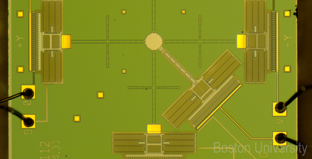
Image caption: Microscopic tools such as this nanoscale “atom writer” can be used to fabricate minuscule light-manipulating structures on surfaces. DARPA has selected 10 performers for its Atoms to Product (A2P) program whose goal is to develop technologies and processes to assemble nanometer-scale pieces—whose dimensions are near the size of atoms—into systems, components, or materials that are at least millimeter-scale in size. (Image credit: Boston University)

Here’s more about the projects and the performers (proponents) from the A2P performers page on the DARPA website,

Nanometer to Millimeter in a Single System – Embody, Draper and Voxtel

Current methods to treat ligament injuries in warfighters [also known as, soldiers]—which account for a significant portion of reported injuries—often fail to restore pre-injury performance, due to surgical complexities and an inadequate supply of donor tissue. Embody is developing reinforced collagen nanofibers that mimic natural ligaments and replicate the biological and biomechanical properties of native tissue. Embody aims to create a new standard of care and restore pre-injury performance for warfighters and sports injury patients at a 50% reduction compared to current costs.

Radio Frequency (RF) systems (e.g., cell phones, GPS) have performance limits due to alternating current loss. In lower frequency power systems this is addressed by braiding the wires, but this is not currently possibly in cell phones due to an inability to manufacture sufficiently small braided wires. Draper is developing submicron wires that can be braided using DNA self-assembly methods. If successful, portable RF systems will be more power efficient and able to send 10 times more information in a given channel.

For seamless control of structures, physics and surface chemistry—from the atomic-level to the meter-level—Voxtel Inc. and partner Oregon State University are developing an efficient, high-rate, fluid-based manufacturing process designed to imitate nature’s ability to manufacture complex multimaterial products across scales. Historically, challenges relating to the cost of atomic-level control, production speed, and printing capability have been effectively insurmountable. This team’s new process will combine synthesis and delivery of materials into a massively parallel inkjet operation that draws from nature to achieve a DNA-like mediated assembly. The goal is to assemble complex, 3-D multimaterial mixed organic and inorganic products quickly and cost-effectively—directly from atoms.

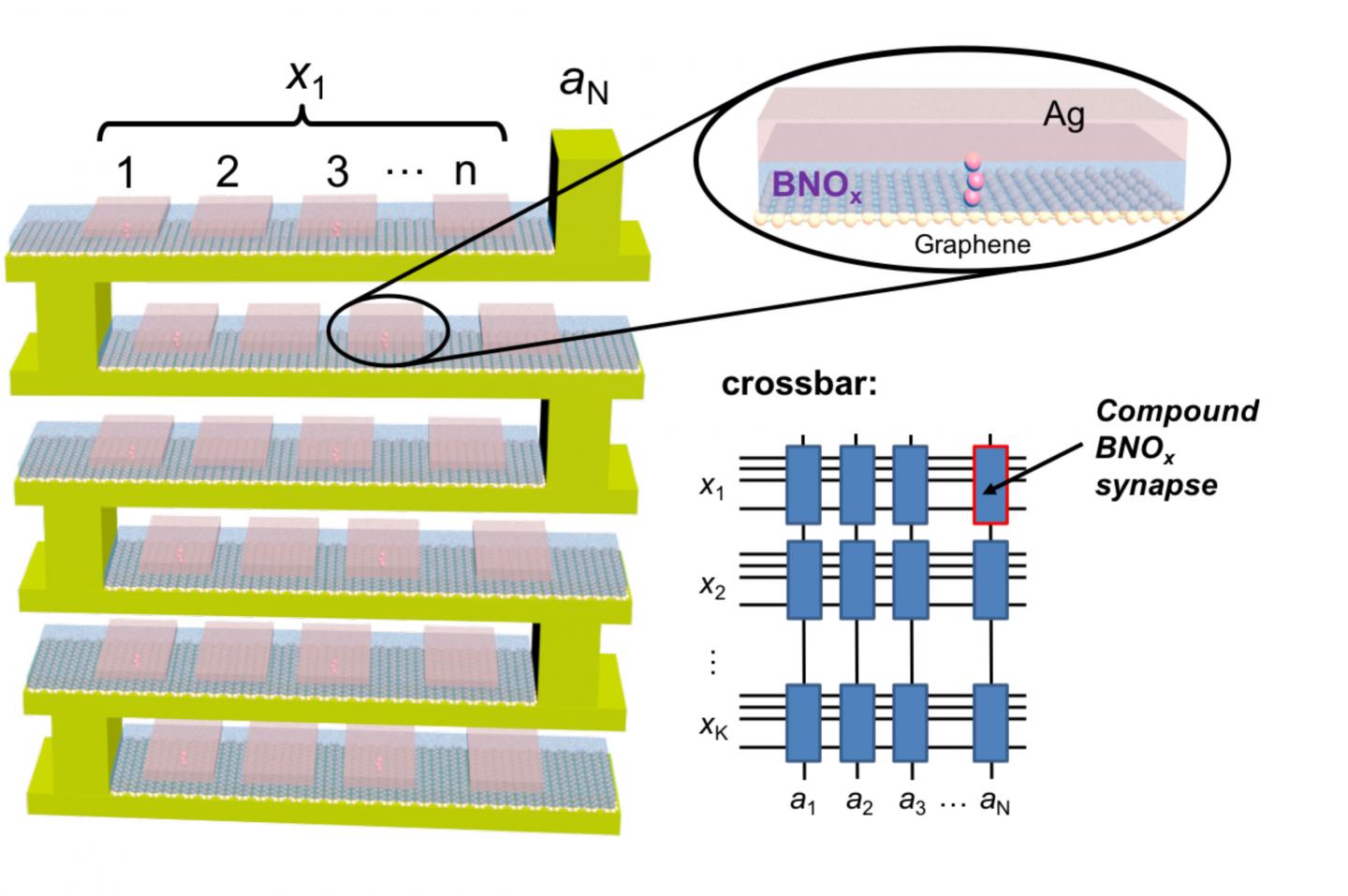
Optical Metamaterial Assembly – Boston University, University of Notre Dame, HRL and PARC.

Nanoscale devices have demonstrated nearly unlimited power and functionality, but there hasn’t been a general- purpose, high-volume, low-cost method for building them. Boston University is developing an atomic calligraphy technique that can spray paint atoms with nanometer precision to build tunable optical metamaterials for the photonic battlefield. If successful, this capability could enhance the survivability of a wide range of military platforms, providing advanced camouflage and other optical illusions in the visual range much as stealth technology has enabled in the radar range.

The University of Notre Dame is developing massively parallel nanomanufacturing strategies to overcome the requirement today that most optical metamaterials must be fabricated in “one-off” operations. The Notre Dame project aims to design and build optical metamaterials that can be reconfigured to rapidly provide on-demand, customized optical capabilities. The aim is to use holographic traps to produce optical “tiles” that can be assembled into a myriad of functional forms and further customized by single-atom electrochemistry. Integrating these materials on surfaces and within devices could provide both warfighters and platforms with transformational survivability.

HRL Laboratories is working on a fast, scalable and material-agnostic process for improving infrared (IR) reflectivity of materials. Current IR-reflective materials have limited use, because reflectivity is highly dependent on the specific angle at which light hits the material. HRL is developing a technique for allowing tailorable infrared reflectivity across a variety of materials. If successful, the process will enable manufacturable materials with up to 98% IR reflectivity at all incident angles.

PARC is working on building the first digital MicroAssembly Printer, where the “inks” are micrometer-size particles and the “image” outputs are centimeter-scale and larger assemblies. The goal is to print smart materials with the throughput and cost of laser printers, but with the precision and functionality of nanotechnology. If successful, the printer would enable the short-run production of large, engineered, customized microstructures, such as metamaterials with unique responses for secure communications, surveillance and electronic warfare.

Flexible, General Purpose Assembly – Zyvex, SRI, and Harvard.

Zyvex aims to create nano-functional micron-scale devices using customizable and scalable manufacturing that is top-down and atomically precise. These high-performance electronic, optical, and nano-mechanical components would be assembled by SRI micro-robots into fully-functional devices and sub-systems such as ultra-sensitive sensors for threat detection, quantum communication devices, and atomic clocks the size of a grain of sand.

SRI’s Levitated Microfactories will seek to combine the precision of MEMS [micro-electromechanical systems] flexures with the versatility and range of pick-and-place robots and the scalability of swarms [an idea Michael Crichton used in his 2002 novel Prey to induce horror] to assemble and electrically connect micron and millimeter components to build stronger materials, faster electronics, and better sensors.

Many high-impact, minimally invasive surgical techniques are currently performed only by elite surgeons due to the lack of tactile feedback at such small scales relative to what is experienced during conventional surgical procedures. Harvard is developing a new manufacturing paradigm for millimeter-scale surgical tools using low-cost 2D layer-by-layer processes and assembly by folding, resulting in arbitrarily complex meso-scale 3D devices. The goal is for these novel tools to restore the necessary tactile feedback and thereby nurture a new degree of dexterity to perform otherwise demanding micro- and minimally invasive surgeries, and thus expand the availability of life-saving procedures.

Sidebar

‘Sidebar’ is my way of indicating these comments have little to do with the matter at hand but could be interesting factoids for you.

First, Zyvex Labs was last mentioned here in a Sept. 10, 2014 posting titled: OCSiAL will not be acquiring Zyvex. Notice that this  announcement was made shortly after DARPA’s A2P program was announced and that OCSiAL is one of RUSNANO’s (a Russian funding agency focused on nanotechnology) portfolio companies (see my Oct. 23, 2015 posting for more).

HRL Laboratories, mentioned here in an April 19, 2012 posting mostly concerned with memristors (nanoscale devices that mimic neural or synaptic plasticity), has its roots in Howard Hughes’s research laboratories as noted in the posting. In 2012, HRL was involved in another DARPA project, SyNAPSE.

Finally and minimally, PARC also known as, Xerox PARC, was made famous by Steven Jobs and Steve Wozniak when they set up their own company (Apple) basing their products on innovations that PARC had rejected. There are other versions of the story and one by Malcolm Gladwell for the New Yorker May 16, 2011 issue which presents a more complicated and, at times, contradictory version of that particular ‘origins’ story.

Brain-on-a-chip 2014 survey/overview

Michael Berger has written another of his Nanowerk Spotlight articles focussing on neuromorphic engineering and the concept of a brain-on-a-chip bringing it up-to-date April 2014 style.

It’s a topic he and I have been following (separately) for years. Berger’s April 4, 2014 Brain-on-a-chip Spotlight article provides a very welcome overview of the international neuromorphic engineering effort (Note: Links have been removed),

Constructing realistic simulations of the human brain is a key goal of the Human Brain Project, a massive European-led research project that commenced in 2013.

The Human Brain Project is a large-scale, scientific collaborative project, which aims to gather all existing knowledge about the human brain, build multi-scale models of the brain that integrate this knowledge and use these models to simulate the brain on supercomputers. The resulting “virtual brain” offers the prospect of a fundamentally new and improved understanding of the human brain, opening the way for better treatments for brain diseases and for novel, brain-like computing technologies.

Several years ago, another European project named FACETS (Fast Analog Computing with Emergent Transient States) completed an exhaustive study of neurons to find out exactly how they work, how they connect to each other and how the network can ‘learn’ to do new things. One of the outcomes of the project was PyNN, a simulator-independent language for building neuronal network models.

Scientists have great expectations that nanotechnologies will bring them closer to the goal of creating computer systems that can simulate and emulate the brain’s abilities for sensation, perception, action, interaction and cognition while rivaling its low power consumption and compact size – basically a brain-on-a-chip. Already, scientists are working hard on laying the foundations for what is called neuromorphic engineering – a new interdisciplinary discipline that includes nanotechnologies and whose goal is to design artificial neural systems with physical architectures similar to biological nervous systems.

Several research projects funded with millions of dollars are at work with the goal of developing brain-inspired computer architectures or virtual brains: DARPA’s SyNAPSE, the EU’s BrainScaleS (a successor to FACETS), or the Blue Brain project (one of the predecessors of the Human Brain Project) at Switzerland’s EPFL [École Polytechnique Fédérale de Lausanne].

Berger goes on to describe the raison d’être for neuromorphic engineering (attempts to mimic biological brains),

Programmable machines are limited not only by their computational capacity, but also by an architecture requiring (human-derived) algorithms to both describe and process information from their environment. In contrast, biological neural systems (e.g., brains) autonomously process information in complex environments by automatically learning relevant and probabilistically stable features and associations. Since real world systems are always many body problems with infinite combinatorial complexity, neuromorphic electronic machines would be preferable in a host of applications – but useful and practical implementations do not yet exist.

Researchers are mostly interested in emulating neural plasticity (aka synaptic plasticity), from Berger’s April 4, 2014 article,

Independent from military-inspired research like DARPA’s, nanotechnology researchers in France have developed a hybrid nanoparticle-organic transistor that can mimic the main functionalities of a synapse. This organic transistor, based on pentacene and gold nanoparticles and termed NOMFET (Nanoparticle Organic Memory Field-Effect Transistor), has opened the way to new generations of neuro-inspired computers, capable of responding in a manner similar to the nervous system  (read more: “Scientists use nanotechnology to try building computers modeled after the brain”).

One of the key components of any neuromorphic effort, and its starting point, is the design of artificial synapses. Synapses dominate the architecture of the brain and are responsible for massive parallelism, structural plasticity, and robustness of the brain. They are also crucial to biological computations that underlie perception and learning. Therefore, a compact nanoelectronic device emulating the functions and plasticity of biological synapses will be the most important building block of brain-inspired computational systems.

In 2011, a team at Stanford University demonstrates a new single element nanoscale device, based on the successfully commercialized phase change material technology, emulating the functionality and the plasticity of biological synapses. In their work, the Stanford team demonstrated a single element electronic synapse with the capability of both the modulation of the time constant and the realization of the different synaptic plasticity forms while consuming picojoule level energy for its operation (read more: “Brain-inspired computing with nanoelectronic programmable synapses”).

Berger does mention memristors but not in any great detail in this article,

Researchers have also suggested that memristor devices are capable of emulating the biological synapses with properly designed CMOS neuron components. A memristor is a two-terminal electronic device whose conductance can be precisely modulated by charge or flux through it. It has the special property that its resistance can be programmed (resistor) and subsequently remains stored (memory).

One research project already demonstrated that a memristor can connect conventional circuits and support a process that is the basis for memory and learning in biological systems (read more: “Nanotechnology’s road to artificial brains”).

You can find a number of memristor articles here including these: Memristors have always been with us from June 14, 2013; How to use a memristor to create an artificial brain from Feb. 26, 2013; Electrochemistry of memristors in a critique of the 2008 discovery from Sept. 6, 2012; and many more (type ‘memristor’ into the blog search box and you should receive many postings or alternatively, you can try ‘artificial brains’ if you want everything I have on artificial brains).

Getting back to Berger’s April 4, 2014 article, he mentions one more approach and this one stands out,

A completely different – and revolutionary – human brain model has been designed by researchers in Japan who introduced the concept of a new class of computer which does not use any circuit or logic gate. This artificial brain-building project differs from all others in the world. It does not use logic-gate based computing within the framework of Turing. The decision-making protocol is not a logical reduction of decision rather projection of frequency fractal operations in a real space, it is an engineering perspective of Gödel’s incompleteness theorem.

Berger wrote about this work in much more detail in a Feb. 10, 2014 Nanowerk Spotlight article titled: Brain jelly – design and construction of an organic, brain-like computer, (Note: Links have been removed),

In a previous Nanowerk Spotlight we reported on the concept of a full-fledged massively parallel organic computer at the nanoscale that uses extremely low power (“Will brain-like evolutionary circuit lead to intelligent computers?”). In this work, the researchers created a process of circuit evolution similar to the human brain in an organic molecular layer. This was the first time that such a brain-like ‘evolutionary’ circuit had been realized.

The research team, led by Dr. Anirban Bandyopadhyay, a senior researcher at the Advanced Nano Characterization Center at the National Institute of Materials Science (NIMS) in Tsukuba, Japan, has now finalized their human brain model and introduced the concept of a new class of computer which does not use any circuit or logic gate.

In a new open-access paper published online on January 27, 2014, in Information (“Design and Construction of a Brain-Like Computer: A New Class of Frequency-Fractal Computing Using Wireless Communication in a Supramolecular Organic, Inorganic System”), Bandyopadhyay and his team now describe the fundamental computing principle of a frequency fractal brain like computer.

“Our artificial brain-building project differs from all others in the world for several reasons,” Bandyopadhyay explains to Nanowerk. He lists the four major distinctions:
1) We do not use logic gate based computing within the framework of Turing, our decision-making protocol is not a logical reduction of decision rather projection of frequency fractal operations in a real space, it is an engineering perspective of Gödel’s incompleteness theorem.
2) We do not need to write any software, the argument and basic phase transition for decision-making, ‘if-then’ arguments and the transformation of one set of arguments into another self-assemble and expand spontaneously, the system holds an astronomically large number of ‘if’ arguments and its associative ‘then’ situations.
3) We use ‘spontaneous reply back’, via wireless communication using a unique resonance band coupling mode, not conventional antenna-receiver model, since fractal based non-radiative power management is used, the power expense is negligible.
4) We have carried out our own single DNA, single protein molecule and single brain microtubule neurophysiological study to develop our own Human brain model.

I encourage people to read Berger’s articles on this topic as they provide excellent information and links to much more. Curiously (mind you, it is easy to miss something), he does not mention James Gimzewski’s work at the University of California at Los Angeles (UCLA). Working with colleagues from the National Institute for Materials Science in Japan, Gimzewski published a paper about “two-, three-terminal WO3-x-based nanoionic devices capable of a broad range of neuromorphic and electrical functions”. You can find out more about the paper in my Dec. 24, 2012 posting titled: Synaptic electronics.

As for the ‘brain jelly’ paper, here’s a link to and a citation for it,

Design and Construction of a Brain-Like Computer: A New Class of Frequency-Fractal Computing Using Wireless Communication in a Supramolecular Organic, Inorganic System by Subrata Ghoshemail, Krishna Aswaniemail, Surabhi Singhemail, Satyajit Sahuemail, Daisuke Fujitaemail and Anirban Bandyopadhyay. Information 2014, 5(1), 28-100; doi:10.3390/info5010028

It’s an open access paper.

As for anyone who’s curious about why the US BRAIN initiative ((Brain Research through Advancing Innovative Neurotechnologies, also referred to as the Brain Activity Map Project) is not mentioned, I believe that’s because it’s focussed on biological brains exclusively at this point (you can check its Wikipedia entry to confirm).

Anirban Bandyopadhyay was last mentioned here in a January 16, 2014 posting titled: Controversial theory of consciousness confirmed (maybe) in  the context of a presentation in Amsterdam, Netherlands.