Tag Archives: artificial brain

Spintronics-based artificial intelligence

Courtesy: Tohoku University

Japanese researchers have managed to mimic a synapse (artificial neural network) with a spintronics-based device according to a Dec. 19, 2016 Tohoku University press release (also on EurekAlert but dated Dec. 20, 2016),

Researchers at Tohoku University have, for the first time, successfully demonstrated the basic operation of spintronics-based artificial intelligence.

Artificial intelligence, which emulates the information processing function of the brain that can quickly execute complex and complicated tasks such as image recognition and weather prediction, has attracted growing attention and has already been partly put to practical use.

The currently-used artificial intelligence works on the conventional framework of semiconductor-based integrated circuit technology. However, this lacks the compactness and low-power feature of the human brain. To overcome this challenge, the implementation of a single solid-state device that plays the role of a synapse is highly promising.

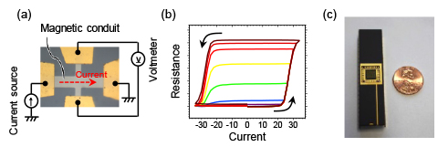
The Tohoku University research group of Professor Hideo Ohno, Professor Shigeo Sato, Professor Yoshihiko Horio, Associate Professor Shunsuke Fukami and Assistant Professor Hisanao Akima developed an artificial neural network in which their recently-developed spintronic devices, comprising micro-scale magnetic material, are employed (Fig. 1). The used spintronic device is capable of memorizing arbitral values between 0 and 1 in an analogue manner unlike the conventional magnetic devices, and thus perform the learning function, which is served by synapses in the brain.

Using the developed network (Fig. 2), the researchers examined an associative memory operation, which is not readily executed by conventional computers. Through the multiple trials, they confirmed that the spintronic devices have a learning ability with which the developed artificial neural network can successfully associate memorized patterns (Fig. 3) from their input noisy versions just like the human brain can.

The proof-of-concept demonstration in this research is expected to open new horizons in artificial intelligence technology – one which is of a compact size, and which simultaneously achieves fast-processing capabilities and ultralow-power consumption. These features should enable the artificial intelligence to be used in a broad range of societal applications such as image/voice recognition, wearable terminals, sensor networks and nursing-care robots.

Here are Fig. 1 and Fig. 2, as mentioned in the press release,

Fig. 1. (a) Optical photograph of a fabricated spintronic device that serves as artificial synapse in the present demonstration. Measurement circuit for the resistance switching is also shown. (b) Measured relation between the resistance of the device and applied current, showing analogue-like resistance variation. (c) Photograph of spintronic device array mounted on a ceramic package, which is used for the developed artificial neural network. Courtesy: Tohoku University

Fig. 2. Block diagram of developed artificial neural network, consisting of PC, FPGA, and array of spintronics (spin-orbit torque; SOT) devices. Courtesy: Tohoku University

Here`s a link to and a citation for the paper,

Analogue spin–orbit torque device for artificial-neural-network-based associative memory operation by William A. Borders, Hisanao Akima1, Shunsuke Fukami, Satoshi Moriya, Shouta Kurihara, Yoshihiko Horio, Shigeo Sato, and Hideo Ohno. Applied Physics Express, Volume 10, Number 1 https://doi.org/10.7567/APEX.10.013007. Published 20 December 2016

© 2017 The Japan Society of Applied Physics

This is an open access paper.

For anyone interested in my other posts on memristors, artificial brains, and artificial intelligence, you can search this blog for those terms  and/or Neuromorphic Engineering in the Categories section.

A new memristor circuit

Apparently engineers at the University of Massachusetts at Amherst have developed a new kind of memristor. A Sept. 29, 2016 news item on Nanowerk makes the announcement (Note: A link has been removed),

Engineers at the University of Massachusetts Amherst are leading a research team that is developing a new type of nanodevice for computer microprocessors that can mimic the functioning of a biological synapse—the place where a signal passes from one nerve cell to another in the body. The work is featured in the advance online publication of Nature Materials (“Memristors with diffusive dynamics as synaptic emulators for neuromorphic computing”).

Such neuromorphic computing in which microprocessors are configured more like human brains is one of the most promising transformative computing technologies currently under study.

While it doesn’t sound different from any other memristor, that’s misleading. Do read on. A Sept. 27, 2016 University of Massachusetts at Amherst news release, which originated the news item, provides more detail about the researchers and the work,

J. Joshua Yang and Qiangfei Xia are professors in the electrical and computer engineering department in the UMass Amherst College of Engineering. Yang describes the research as part of collaborative work on a new type of memristive device.

Memristive devices are electrical resistance switches that can alter their resistance based on the history of applied voltage and current. These devices can store and process information and offer several key performance characteristics that exceed conventional integrated circuit technology.

“Memristors have become a leading candidate to enable neuromorphic computing by reproducing the functions in biological synapses and neurons in a neural network system, while providing advantages in energy and size,” the researchers say.

Neuromorphic computing—meaning microprocessors configured more like human brains than like traditional computer chips—is one of the most promising transformative computing technologies currently under intensive study. Xia says, “This work opens a new avenue of neuromorphic computing hardware based on memristors.”

They say that most previous work in this field with memristors has not implemented diffusive dynamics without using large standard technology found in integrated circuits commonly used in microprocessors, microcontrollers, static random access memory and other digital logic circuits.

The researchers say they proposed and demonstrated a bio-inspired solution to the diffusive dynamics that is fundamentally different from the standard technology for integrated circuits while sharing great similarities with synapses. They say, “Specifically, we developed a diffusive-type memristor where diffusion of atoms offers a similar dynamics [?] and the needed time-scales as its bio-counterpart, leading to a more faithful emulation of actual synapses, i.e., a true synaptic emulator.”

The researchers say, “The results here provide an encouraging pathway toward synaptic emulation using diffusive memristors for neuromorphic computing.”

Here’s a link to and a citation for the paper,

Memristors with diffusive dynamics as synaptic emulators for neuromorphic computing by Zhongrui Wang, Saumil Joshi, Sergey E. Savel’ev, Hao Jiang, Rivu Midya, Peng Lin, Miao Hu, Ning Ge, John Paul Strachan, Zhiyong Li, Qing Wu, Mark Barnell, Geng-Lin Li, Huolin L. Xin, R. Stanley Williams [emphasis mine], Qiangfei Xia, & J. Joshua Yang. Nature Materials (2016) doi:10.1038/nmat4756 Published online 26 September 2016

This paper is behind a paywall.

I’ve emphasized R. Stanley Williams’ name as he was the lead researcher on the HP Labs team that proved Leon Chua’s 1971 theory about the memristor and exerted engineering control of the memristor in 2008. (Bernard Widrow, in the 1960s,  predicted and proved the existence of something he termed a ‘memistor’. Chua arrived at his ‘memristor’ theory independently.)

Austin Silver in a Sept. 29, 2016 posting on The Human OS blog (on the IEEE [Institute of Electrical and Electronics Engineers] website) delves into this latest memristor research (Note: Links have been removed),

In research published in Nature Materials on 26 September [2016], Yang and his team mimicked a crucial underlying component of how synaptic connections get stronger or weaker: the flow of calcium.

The movement of calcium into or out of the neuronal membrane, neuroscientists have found, directly affects the connection. Chemical processes move the calcium in and out— triggering a long-term change in the synapses’ strength. 2015 research in ACS NanoLetters and Advanced Functional Materials discovered that types of memristors can simulate some of the calcium behavior, but not all.

In the new research, Yang combined two types of memristors in series to create an artificial synapse. The hybrid device more closely mimics biological synapse behavior—the calcium flow in particular, Yang says.

The new memristor used–called a diffusive memristor because atoms in the resistive material move even without an applied voltage when the device is in the high resistance state—was a dielectic film sandwiched between Pt [platinum] or Au [gold] electrodes. The film contained Ag [silver] nanoparticles, which would play the role of calcium in the experiments.

By tracking the movement of the silver nanoparticles inside the diffusive memristor, the researchers noticed a striking similarity to how calcium functions in biological systems.

A voltage pulse to the hybrid device drove silver into the gap between the diffusive memristor’s two electrodes–creating a filament bridge. After the pulse died away, the filament started to break and the silver moved back— resistance increased.

Like the case with calcium, a force made silver go in and a force made silver go out.

To complete the artificial synapse, the researchers connected the diffusive memristor in series to another type of memristor that had been studied before.

When presented with a sequence of voltage pulses with particular timing, the artificial synapse showed the kind of long-term strengthening behavior a real synapse would, according to the researchers. “We think it is sort of a real emulation, rather than simulation because they have the physical similarity,” Yang says.

I was glad to find some additional technical detail about this new memristor and to find the Human OS blog, which is new to me and according to its home page is a “biomedical blog, featuring the wearable sensors, big data analytics, and implanted devices that enable new ventures in personalized medicine.”

Memristive capabilities from IBM (International Business Machines)

Does memristive mean it’s like a memristor but it’s not one? In any event, IBM is claiming some new ground in the world of cognitive computing (also known as, neuromorphic computing).

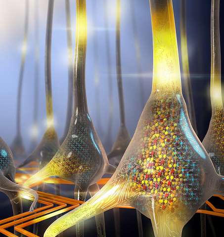
An artistic rendering of a population of stochastic phase-change neurons which appears on the cover of Nature Nanotechnology, 3 August 2016. (Credit: IBM Research)

An artistic rendering of a population of stochastic phase-change neurons which appears on the cover of Nature Nanotechnology, 3 August 2016. (Credit: IBM Research)

From an Aug. 3, 2016 news item on phys.org,

IBM scientists have created randomly spiking neurons using phase-change materials to store and process data. This demonstration marks a significant step forward in the development of energy-efficient, ultra-dense integrated neuromorphic technologies for applications in cognitive computing.

Inspired by the way the biological brain functions, scientists have theorized for decades that it should be possible to imitate the versatile computational capabilities of large populations of neurons. However, doing so at densities and with a power budget that would be comparable to those seen in biology has been a significant challenge, until now.

“We have been researching phase-change materials for memory applications for over a decade, and our progress in the past 24 months has been remarkable,” said IBM Fellow Evangelos Eleftheriou. “In this period, we have discovered and published new memory techniques, including projected memory, stored 3 bits per cell in phase-change memory for the first time, and now are demonstrating the powerful capabilities of phase-change-based artificial neurons, which can perform various computational primitives such as data-correlation detection and unsupervised learning at high speeds using very little energy.”

An Aug. 3, 2016 IBM news release, which originated the news item, expands on the theme,

The artificial neurons designed by IBM scientists in Zurich consist of phase-change materials, including germanium antimony telluride, which exhibit two stable states, an amorphous one (without a clearly defined structure) and a crystalline one (with structure). These materials are the basis of re-writable Blu-ray discs. However, the artificial neurons do not store digital information; they are analog, just like the synapses and neurons in our biological brain.

In the published demonstration, the team applied a series of electrical pulses to the artificial neurons, which resulted in the progressive crystallization of the phase-change material, ultimately causing the neuron to fire. In neuroscience, this function is known as the integrate-and-fire property of biological neurons. This is the foundation for event-based computation and, in principle, is similar to how our brain triggers a response when we touch something hot.

Exploiting this integrate-and-fire property, even a single neuron can be used to detect patterns and discover correlations in real-time streams of event-based data. For example, in the Internet of Things, sensors can collect and analyze volumes of weather data collected at the edge for faster forecasts. The artificial neurons could be used to detect patterns in financial transactions to find discrepancies or use data from social media to discover new cultural trends in real time. Large populations of these high-speed, low-energy nano-scale neurons could also be used in neuromorphic coprocessors with co-located memory and processing units.

IBM scientists have organized hundreds of artificial neurons into populations and used them to represent fast and complex signals. Moreover, the artificial neurons have been shown to sustain billions of switching cycles, which would correspond to multiple years of operation at an update frequency of 100 Hz. The energy required for each neuron update was less than five picojoule and the average power less than 120 microwatts — for comparison, 60 million microwatts power a 60 watt lightbulb.

“Populations of stochastic phase-change neurons, combined with other nanoscale computational elements such as artificial synapses, could be a key enabler for the creation of a new generation of extremely dense neuromorphic computing systems,” said Tomas Tuma, a co-author of the paper.

Here’s a link to and a citation for the paper,

Stochastic phase-change neurons by Tomas Tuma, Angeliki Pantazi, Manuel Le Gallo, Abu Sebastian, & Evangelos Eleftheriou. Nature Nanotechnology  11, 693–699 (2016) doi:10.1038/nnano.2016.70 Published online 16 May 2016

I gather IBM waited for the print version of the paper before publicizing the work. The online version is behind paper. For those who can’t get past the paywall, there is a video offering a demonstration of sorts,

For the interested, the US government recently issued a white paper on neuromorphic computing (my Aug. 22, 2016 post).

This team has published a paper that has a similar theme to the one in Nature Nanotechnology,

All-memristive neuromorphic computing with level-tuned neurons by Angeliki Pantazi, Stanisław Woźniak, Tomas Tuma, and Evangelos Eleftheriou. Nanotechnology, Volume 27, Number 35  DOI: 10.1088/0957-4484/27/35/355205 Published 26 July 2016

© 2016 IOP Publishing Ltd

This paper is open access.

An Aug. 18, 2016 news piece by Lisa Zyga for phys.org provides a summary of the research in the July 2016 published paper.

US white paper on neuromorphic computing (or the nanotechnology-inspired Grand Challenge for future computing)

The US has embarked on a number of what is called “Grand Challenges.” I first came across the concept when reading about the Bill and Melinda Gates (of Microsoft fame) Foundation. I gather these challenges are intended to provide funding for research that advances bold visions.

There is the US National Strategic Computing Initiative established on July 29, 2015 and its first anniversary results were announced one year to the day later. Within that initiative a nanotechnology-inspired Grand Challenge for Future Computing was issued and, according to a July 29, 2016 news item on Nanowerk, a white paper on the topic has been issued (Note: A link has been removed),

Today [July 29, 2016), Federal agencies participating in the National Nanotechnology Initiative (NNI) released a white paper (pdf) describing the collective Federal vision for the emerging and innovative solutions needed to realize the Nanotechnology-Inspired Grand Challenge for Future Computing.

The grand challenge, announced on October 20, 2015, is to “create a new type of computer that can proactively interpret and learn from data, solve unfamiliar problems using what it has learned, and operate with the energy efficiency of the human brain.” The white paper describes the technical priorities shared by the agencies, highlights the challenges and opportunities associated with these priorities, and presents a guiding vision for the research and development (R&D) needed to achieve key technical goals. By coordinating and collaborating across multiple levels of government, industry, academia, and nonprofit organizations, the nanotechnology and computer science communities can look beyond the decades-old approach to computing based on the von Neumann architecture and chart a new path that will continue the rapid pace of innovation beyond the next decade.

A July 29, 2016 US National Nanotechnology Coordination Office news release, which originated the news item, further and succinctly describes the contents of the paper,

“Materials and devices for computing have been and will continue to be a key application domain in the field of nanotechnology. As evident by the R&D topics highlighted in the white paper, this challenge will require the convergence of nanotechnology, neuroscience, and computer science to create a whole new paradigm for low-power computing with revolutionary, brain-like capabilities,” said Dr. Michael Meador, Director of the National Nanotechnology Coordination Office. …

The white paper was produced as a collaboration by technical staff at the Department of Energy, the National Science Foundation, the Department of Defense, the National Institute of Standards and Technology, and the Intelligence Community. …

The white paper titled “A Federal Vision for Future Computing: A Nanotechnology-Inspired Grand Challenge” is 15 pp. and it offers tidbits such as this (Note: Footnotes not included),

A new materials base may be needed for future electronic hardware. While most of today’s electronics use silicon, this approach is unsustainable if billions of disposable and short-lived sensor nodes are needed for the coming Internet-of-Things (IoT). To what extent can the materials base for the implementation of future information technology (IT) components and systems support sustainability through recycling and bio-degradability? More sustainable materials, such as compostable or biodegradable systems (polymers, paper, etc.) that can be recycled or reused,  may play an important role. The potential role for such alternative materials in the fabrication of integrated systems needs to be explored as well. [p. 5]

The basic architecture of computers today is essentially the same as those built in the 1940s—the von Neumann architecture—with separate compute, high-speed memory, and high-density storage components that are electronically interconnected. However, it is well known that continued performance increases using this architecture are not feasible in the long term, with power density constraints being one of the fundamental roadblocks.7 Further advances in the current approach using multiple cores, chip multiprocessors, and associated architectures are plagued by challenges in software and programming models. Thus,  research and development is required in radically new and different computing architectures involving processors, memory, input-output devices, and how they behave and are interconnected. [p. 7]

Neuroscience research suggests that the brain is a complex, high-performance computing system with low energy consumption and incredible parallelism. A highly plastic and flexible organ, the human brain is able to grow new neurons, synapses, and connections to cope with an ever-changing environment. Energy efficiency, growth, and flexibility occur at all scales, from molecular to cellular, and allow the brain, from early to late stage, to never stop learning and to act with proactive intelligence in both familiar and novel situations. Understanding how these mechanisms work and cooperate within and across scales has the potential to offer tremendous technical insights and novel engineering frameworks for materials, devices, and systems seeking to perform efficient and autonomous computing. This research focus area is the most synergistic with the national BRAIN Initiative. However, unlike the BRAIN Initiative, where the goal is to map the network connectivity of the brain, the objective here is to understand the nature, methods, and mechanisms for computation,  and how the brain performs some of its tasks. Even within this broad paradigm,  one can loosely distinguish between neuromorphic computing and artificial neural network (ANN) approaches. The goal of neuromorphic computing is oriented towards a hardware approach to reverse engineering the computational architecture of the brain. On the other hand, ANNs include algorithmic approaches arising from machinelearning,  which in turn could leverage advancements and understanding in neuroscience as well as novel cognitive, mathematical, and statistical techniques. Indeed, the ultimate intelligent systems may as well be the result of merging existing ANN (e.g., deep learning) and bio-inspired techniques. [p. 8]

As government documents go, this is quite readable.

For anyone interested in learning more about the future federal plans for computing in the US, there is a July 29, 2016 posting on the White House blog celebrating the first year of the US National Strategic Computing Initiative Strategic Plan (29 pp. PDF; awkward but that is the title).

Artificial synapse rivals biological synapse in energy consumption

How can we make computers be like biological brains which do so much work and use so little power? It’s a question scientists from many countries are trying to answer and it seems South Korean scientists are proposing an answer. From a June 20, 2016 news item on Nanowerk,

News) Creation of an artificial intelligence system that fully emulates the functions of a human brain has long been a dream of scientists. A brain has many superior functions as compared with super computers, even though it has light weight, small volume, and consumes extremely low energy. This is required to construct an artificial neural network, in which a huge amount (1014)) of synapses is needed.

Most recently, great efforts have been made to realize synaptic functions in single electronic devices, such as using resistive random access memory (RRAM), phase change memory (PCM), conductive bridges, and synaptic transistors. Artificial synapses based on highly aligned nanostructures are still desired for the construction of a highly-integrated artificial neural network.

Prof. Tae-Woo Lee, research professor Wentao Xu, and Dr. Sung-Yong Min with the Dept. of Materials Science and Engineering at POSTECH [Pohang University of Science & Technology, South Korea] have succeeded in fabricating an organic nanofiber (ONF) electronic device that emulates not only the important working principles and energy consumption of biological synapses but also the morphology. …

A June 20, 2016 Pohang University of Science & Technology (POSTECH) news release on EurekAlert, which originated the news item, describes the work in more detail,

The morphology of ONFs is very similar to that of nerve fibers, which form crisscrossing grids to enable the high memory density of a human brain. Especially, based on the e-Nanowire printing technique, highly-aligned ONFs can be massively produced with precise control over alignment and dimension. This morphology potentially enables the future construction of high-density memory of a neuromorphic system.

Important working principles of a biological synapse have been emulated, such as paired-pulse facilitation (PPF), short-term plasticity (STP), long-term plasticity (LTP), spike-timing dependent plasticity (STDP), and spike-rate dependent plasticity (SRDP). Most amazingly, energy consumption of the device can be reduced to a femtojoule level per synaptic event, which is a value magnitudes lower than previous reports. It rivals that of a biological synapse. In addition, the organic artificial synapse devices not only provide a new research direction in neuromorphic electronics but even open a new era of organic electronics.

This technology will lead to the leap of brain-inspired electronics in both memory density and energy consumption aspects. The artificial synapse developed by Prof. Lee’s research team will provide important potential applications to neuromorphic computing systems and artificial intelligence systems for autonomous cars (or self-driving cars), analysis of big data, cognitive systems, robot control, medical diagnosis, stock trading analysis, remote sensing, and other smart human-interactive systems and machines in the future.

Here’s a link to and a citation for the paper,

Organic core-sheath nanowire artificial synapses with femtojoule energy consumption by Wentao Xu, Sung-Yong Min, Hyunsang Hwang, and Tae-Woo Lee. Science Advances  17 Jun 2016: Vol. 2, no. 6, e1501326 DOI: 10.1126/sciadv.1501326

This paper is open access.

X-rays reveal memristor workings

A June 14, 2016 news item on ScienceDaily focuses on memristors. (It’s been about two months since my last memristor posting on April 22, 2016 regarding electronic synapses and neural networks). This piece announces new insight into how memristors function at the atomic scale,

In experiments at two Department of Energy national labs — SLAC National Accelerator Laboratory and Lawrence Berkeley National Laboratory — scientists at Hewlett Packard Enterprise (HPE) [also referred to as HP Labs or Hewlett Packard Laboratories] have experimentally confirmed critical aspects of how a new type of microelectronic device, the memristor, works at an atomic scale.

This result is an important step in designing these solid-state devices for use in future computer memories that operate much faster, last longer and use less energy than today’s flash memory. …

“We need information like this to be able to design memristors that will succeed commercially,” said Suhas Kumar, an HPE scientist and first author on the group’s technical paper.

A June 13, 2016 SLAC news release, which originated the news item, offers a brief history according to HPE and provides details about the latest work,

The memristor was proposed theoretically [by Dr. Leon Chua] in 1971 as the fourth basic electrical device element alongside the resistor, capacitor and inductor. At its heart is a tiny piece of a transition metal oxide sandwiched between two electrodes. Applying a positive or negative voltage pulse dramatically increases or decreases the memristor’s electrical resistance. This behavior makes it suitable for use as a “non-volatile” computer memory that, like flash memory, can retain its state without being refreshed with additional power.

Over the past decade, an HPE group led by senior fellow R. Stanley Williams has explored memristor designs, materials and behavior in detail. Since 2009 they have used intense synchrotron X-rays to reveal the movements of atoms in memristors during switching. Despite advances in understanding the nature of this switching, critical details that would be important in designing commercially successful circuits  remained controversial. For example, the forces that move the atoms, resulting in dramatic resistance changes during switching, remain under debate.

In recent years, the group examined memristors made with oxides of titanium, tantalum and vanadium. Initial experiments revealed that switching in the tantalum oxide devices could be controlled most easily, so it was chosen for further exploration at two DOE Office of Science User Facilities – SLAC’s Stanford Synchrotron Radiation Lightsource (SSRL) and Berkeley Lab’s Advanced Light Source (ALS).

At ALS, the HPE researchers mapped the positions of oxygen atoms before and after switching. For this, they used a scanning transmission X-ray microscope and an apparatus they built to precisely control the position of their sample and the timing and intensity of the 500-electronvolt ALS X-rays, which were tuned to see oxygen.

The experiments revealed that even weak voltage pulses create a thin conductive path through the memristor. During the pulse the path heats up, which creates a force that pushes oxygen atoms away from the path, making it even more conductive. Reversing the voltage pulse resets the memristor by sucking some of oxygen atoms back into the conducting path, thereby increasing the device’s resistance. The memristor’s resistance changes between 10-fold and 1 million-fold, depending on operating parameters like the voltage-pulse amplitude. This resistance change is dramatic enough to exploit commercially.

To be sure of their conclusion, the researchers also needed to understand if the tantalum atoms were moving along with the oxygen during switching. Imaging tantalum required higher-energy, 10,000-electronvolt X-rays, which they obtained at SSRL’s Beam Line 6-2. In a single session there, they determined that the tantalum remained stationary.

“That sealed the deal, convincing us that our hypothesis was correct,” said HPE scientist Catherine Graves, who had worked at SSRL as a Stanford graduate student. She added that discussions with SLAC experts were critical in guiding the HPE team toward the X-ray techniques that would allow them to see the tantalum accurately.

Kumar said the most promising aspect of the tantalum oxide results was that the scientists saw no degradation in switching over more than a billion voltage pulses of a magnitude suitable for commercial use. He added that this knowledge helped his group build memristors that lasted nearly a billion switching cycles, about a thousand-fold improvement.

“This is much longer endurance than is possible with today’s flash memory devices,” Kumar said. “In addition, we also used much higher voltage pulses to accelerate and observe memristor failures, which is also important in understanding how these devices work. Failures occurred when oxygen atoms were forced so far away that they did not return to their initial positions.”

Beyond memory chips, Kumar says memristors’ rapid switching speed and small size could make them suitable for use in logic circuits. Additional memristor characteristics may also be beneficial in the emerging class of brain-inspired neuromorphic computing circuits.

“Transistors are big and bulky compared to memristors,” he said. “Memristors are also much better suited for creating the neuron-like voltage spikes that characterize neuromorphic circuits.”

The researchers have provided an animation illustrating how memristors can fail,

This animation shows how millions of high-voltage switching cycles can cause memristors to fail. The high-voltage switching eventually creates regions that are permanently rich (blue pits) or deficient (red peaks) in oxygen and cannot be switched back. Switching at lower voltages that would be suitable for commercial devices did not show this performance degradation. These observations allowed the researchers to develop materials processing and operating conditions that improved the memristors’ endurance by nearly a thousand times. (Suhas Kumar) Courtesy: SLAC

This animation shows how millions of high-voltage switching cycles can cause memristors to fail. The high-voltage switching eventually creates regions that are permanently rich (blue pits) or deficient (red peaks) in oxygen and cannot be switched back. Switching at lower voltages that would be suitable for commercial devices did not show this performance degradation. These observations allowed the researchers to develop materials processing and operating conditions that improved the memristors’ endurance by nearly a thousand times. (Suhas Kumar) Courtesy: SLAC

Here’s a link to and a citation for the paper,

Direct Observation of Localized Radial Oxygen Migration in Functioning Tantalum Oxide Memristors by Suhas Kumar, Catherine E. Graves, John Paul Strachan, Emmanuelle Merced Grafals, Arthur L. David Kilcoyne3, Tolek Tyliszczak, Johanna Nelson Weker, Yoshio Nishi, and R. Stanley Williams. Advanced Materials, First published: 2 February 2016; Print: Volume 28, Issue 14 April 13, 2016 Pages 2772–2776 DOI: 10.1002/adma.201505435

This paper is behind a paywall.

Some of the ‘memristor story’ is contested and you can find a brief overview of the discussion in this Wikipedia memristor entry in the section on ‘definition and criticism’. There is also a history of the memristor which dates back to the 19th century featured in my May 22, 2012 posting.

US White House’s grand computing challenge could mean a boost for research into artificial intelligence and brains

An Oct. 20, 2015 posting by Lynn Bergeson on Nanotechnology Now announces a US White House challenge incorporating nanotechnology, computing, and brain research (Note: A link has been removed),

On October 20, 2015, the White House announced a grand challenge to develop transformational computing capabilities by combining innovations in multiple scientific disciplines. See https://www.whitehouse.gov/blog/2015/10/15/nanotechnology-inspired-grand-challenge-future-computing The Office of Science and Technology Policy (OSTP) states that, after considering over 100 responses to its June 17, 2015, request for information, it “is excited to announce the following grand challenge that addresses three Administration priorities — the National Nanotechnology Initiative, the National Strategic Computing Initiative (NSCI), and the BRAIN initiative.” The grand challenge is to “[c]reate a new type of computer that can proactively interpret and learn from data, solve unfamiliar problems using what it has learned, and operate with the energy efficiency of the human brain.”

Here’s where the Oct. 20, 2015 posting, which originated the news item, by Lloyd Whitman, Randy Bryant, and Tom Kalil for the US White House blog gets interesting,

 While it continues to be a national priority to advance conventional digital computing—which has been the engine of the information technology revolution—current technology falls far short of the human brain in terms of both the brain’s sensing and problem-solving abilities and its low power consumption. Many experts predict that fundamental physical limitations will prevent transistor technology from ever matching these twin characteristics. We are therefore challenging the nanotechnology and computer science communities to look beyond the decades-old approach to computing based on the Von Neumann architecture as implemented with transistor-based processors, and chart a new path that will continue the rapid pace of innovation beyond the next decade.

There are growing problems facing the Nation that the new computing capabilities envisioned in this challenge might address, from delivering individualized treatments for disease, to allowing advanced robots to work safely alongside people, to proactively identifying and blocking cyber intrusions. To meet this challenge, major breakthroughs are needed not only in the basic devices that store and process information and the amount of energy they require, but in the way a computer analyzes images, sounds, and patterns; interprets and learns from data; and identifies and solves problems. [emphases mine]

Many of these breakthroughs will require new kinds of nanoscale devices and materials integrated into three-dimensional systems and may take a decade or more to achieve. These nanotechnology innovations will have to be developed in close coordination with new computer architectures, and will likely be informed by our growing understanding of the brain—a remarkable, fault-tolerant system that consumes less power than an incandescent light bulb.

Recent progress in developing novel, low-power methods of sensing and computation—including neuromorphic, magneto-electronic, and analog systems—combined with dramatic advances in neuroscience and cognitive sciences, lead us to believe that this ambitious challenge is now within our reach. …

This is the first time I’ve come across anything that publicly links the BRAIN initiative to computing, artificial intelligence, and artificial brains. (For my own sake, I make an arbitrary distinction between algorithms [artificial intelligence] and devices that simulate neural plasticity [artificial brains].)The emphasis in the past has always been on new strategies for dealing with Parkinson’s and other neurological diseases and conditions.

Computer chips derived in a Darwinian environment

Courtesy: University of Twente

Courtesy: University of Twente

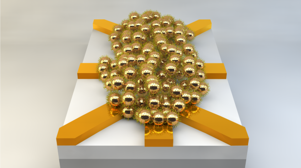
If that ‘computer chip’ looks a brain to you, good, since that’s what the image is intended to illustrate assuming I’ve correctly understood the Sept. 21, 2015 news item on Nanowerk (Note: A link has been removed),

Researchers of the MESA+ Institute for Nanotechnology and the CTIT Institute for ICT Research at the University of Twente in The Netherlands have demonstrated working electronic circuits that have been produced in a radically new way, using methods that resemble Darwinian evolution. The size of these circuits is comparable to the size of their conventional counterparts, but they are much closer to natural networks like the human brain. The findings promise a new generation of powerful, energy-efficient electronics, and have been published in the leading British journal Nature Nanotechnology (“Evolution of a Designless Nanoparticle Network into Reconfigurable Boolean Logic”).

A Sept. 21, 2015 University of Twente press release, which originated the news item, explains why and how they have decided to mimic nature to produce computer chips,

One of the greatest successes of the 20th century has been the development of digital computers. During the last decades these computers have become more and more powerful by integrating ever smaller components on silicon chips. However, it is becoming increasingly hard and extremely expensive to continue this miniaturisation. Current transistors consist of only a handful of atoms. It is a major challenge to produce chips in which the millions of transistors have the same characteristics, and thus to make the chips operate properly. Another drawback is that their energy consumption is reaching unacceptable levels. It is obvious that one has to look for alternative directions, and it is interesting to see what we can learn from nature. Natural evolution has led to powerful ‘computers’ like the human brain, which can solve complex problems in an energy-efficient way. Nature exploits complex networks that can execute many tasks in parallel.

Moving away from designed circuits

The approach of the researchers at the University of Twente is based on methods that resemble those found in Nature. They have used networks of gold nanoparticles for the execution of essential computational tasks. Contrary to conventional electronics, they have moved away from designed circuits. By using ‘designless’ systems, costly design mistakes are avoided. The computational power of their networks is enabled by applying artificial evolution. This evolution takes less than an hour, rather than millions of years. By applying electrical signals, one and the same network can be configured into 16 different logical gates. The evolutionary approach works around – or can even take advantage of – possible material defects that can be fatal in conventional electronics.

Powerful and energy-efficient

It is the first time that scientists have succeeded in this way in realizing robust electronics with dimensions that can compete with commercial technology. According to prof. Wilfred van der Wiel, the realized circuits currently still have limited computing power. “But with this research we have delivered proof of principle: demonstrated that our approach works in practice. By scaling up the system, real added value will be produced in the future. Take for example the efforts to recognize patterns, such as with face recognition. This is very difficult for a regular computer, while humans and possibly also our circuits can do this much better.”  Another important advantage may be that this type of circuitry uses much less energy, both in the production, and during use. The researchers anticipate a wide range of applications, for example in portable electronics and in the medical world.

Here’s a link to and a citation for the paper,

Evolution of a designless nanoparticle network into reconfigurable Boolean logic by S. K. Bose, C. P. Lawrence, Z. Liu, K. S. Makarenko, R. M. J. van Damme, H. J. Broersma, & W. G. van der Wiel. Nature Nanotechnology (2015) doi:10.1038/nnano.2015.207 Published online 21 September 2015

This paper is behind a paywall.

Final comment, this research, especially with the reference to facial recognition, reminds me of memristors and neuromorphic engineering. I have written many times on this topic and you should be able to find most of the material by using ‘memristor’ as your search term in the blog search engine. For the mildly curious, here are links to two recent memristor articles, Knowm (sounds like gnome?) A memristor company with a commercially available product in a Sept. 10, 2015 posting and Memristor, memristor, you are popular in a May 15, 2015 posting.

Researchers at Karolinska Institute (Sweden) build an artificial neuron

Unlike my post earlier today (June 26, 2015) about BrainChip, this is not about neuromorphic engineering (artificial brain), although I imagine this new research from the Karolinska Institute (Institutet) will be of some interest to that community. This research was done in the interest of developing* therapeutic interventions for brain diseases. One aspect of this news item/press release I find particularly interesting is the insistence that “no living parts” were used to create the artificial neuron,

A June 24, 2015 news item on ScienceDaily describes what the artificial neuron can do,

Scientists have managed to build a fully functional neuron by using organic bioelectronics. This artificial neuron contain [sic] no ‘living’ parts, but is capable of mimicking the function of a human nerve cell and communicate in the same way as our own neurons do. [emphasis mine]

A June 24, 2015 Karolinska Institute press release (also on EurekAlert), which originated the news item, describes how neurons communicate in the brain, standard techniques for stimulating neuronal cells, and the scientists’ work on a technique to improve stimulation,

Neurons are isolated from each other and communicate with the help of chemical signals, commonly called neurotransmitters or signal substances. Inside a neuron, these chemical signals are converted to an electrical action potential, which travels along the axon of the neuron until it reaches the end. Here at the synapse, the electrical signal is converted to the release of chemical signals, which via diffusion can relay the signal to the next nerve cell.

To date, the primary technique for neuronal stimulation in human cells is based on electrical stimulation. However, scientists at the Swedish Medical Nanoscience Centre (SMNC) at Karolinska Institutet in collaboration with collegues at Linköping University, have now created an organic bioelectronic device that is capable of receiving chemical signals, which it can then relay to human cells.

“Our artificial neuron is made of conductive polymers and it functions like a human neuron,” says lead investigator Agneta Richter-Dahlfors, professor of cellular microbiology. “The sensing component of the artificial neuron senses a change in chemical signals in one dish, and translates this into an electrical signal. This electrical signal is next translated into the release of the neurotransmitter acetylcholine in a second dish, whose effect on living human cells can be monitored.”

The research team hope that their innovation, presented in the journal Biosensors & Bioelectronics, will improve treatments for neurologial disorders which currently rely on traditional electrical stimulation. The new technique makes it possible to stimulate neurons based on specific chemical signals received from different parts of the body. In the future, this may help physicians to bypass damaged nerve cells and restore neural function.

“Next, we would like to miniaturize this device to enable implantation into the human body,” says Agneta Richer-Dahlfors. “We foresee that in the future, by adding the concept of wireless communication, the biosensor could be placed in one part of the body, and trigger release of neurotransmitters at distant locations. Using such auto-regulated sensing and delivery, or possibly a remote control, new and exciting opportunities for future research and treatment of neurological disorders can be envisaged.”

Here’s a link to and a citation for the paper,

An organic electronic biomimetic neuron enables auto-regulated neuromodulation by Daniel T. Simon, Karin C. Larsson, David Nilsson, Gustav Burström, b, Dagmar Galter, Magnus Berggren, and Agneta Richter-Dahlfors. Biosensors and Bioelectronics Volume 71, 15 September 2015, Pages 359–364         doi:10.1016/j.bios.2015.04.058

This paper is behind a paywall.

As to anyone (other than myself) who may be curious about exactly what they used (other than “living parts”) to create an artificial neuron, there’s the paper’s abstract,

Current therapies for neurological disorders are based on traditional medication and electric stimulation. Here, we present an organic electronic biomimetic neuron, with the capacity to precisely intervene with the underlying malfunctioning signalling pathway using endogenous substances. The fundamental function of neurons, defined as chemical-to-electrical-to-chemical signal transduction, is achieved by connecting enzyme-based amperometric biosensors and organic electronic ion pumps. Selective biosensors transduce chemical signals into an electric current, which regulates electrophoretic delivery of chemical substances without necessitating liquid flow. Biosensors detected neurotransmitters in physiologically relevant ranges of 5–80 µM, showing linear response above 20 µm with approx. 0.1 nA/µM slope. When exceeding defined threshold concentrations, biosensor output signals, connected via custom hardware/software, activated local or distant neurotransmitter delivery from the organic electronic ion pump. Changes of 20 µM glutamate or acetylcholine triggered diffusive delivery of acetylcholine, which activated cells via receptor-mediated signalling. This was observed in real-time by single-cell ratiometric Ca2+ imaging. The results demonstrate the potential of the organic electronic biomimetic neuron in therapies involving long-range neuronal signalling by mimicking the function of projection neurons. Alternatively, conversion of glutamate-induced descending neuromuscular signals into acetylcholine-mediated muscular activation signals may be obtained, applicable for bridging injured sites and active prosthetics.

While it’s true neither are “living parts,” I believe both enzymes and organic electronic ion pumps can be found in biological organisms. The insistence on ‘nonliving’ in the press release suggests that scientists in Europe, if nowhere else, are still quite concerned about any hint that they are working on genetically modified organisms (GMO). It’s ironic when you consider that people blithely use enzyme-based cleaning and beauty products but one can appreciate the* scientists’ caution.

* ‘develop’ changed to ‘developing’ and ‘the’ added on July 3, 2015.

Is it time to invest in a ‘brain chip’ company?

This story take a few twists and turns. First, ‘brain chips’ as they’re sometimes called would allow, theoretically, computers to learn and function like human brains. (Note: There’s another type of ‘brain chip’ which could be implanted in human brains to help deal with diseases such as Parkinson’s and Alzheimer’s. *Today’s [June 26, 2015] earlier posting about an artificial neuron points at some of the work being done in this areas.*)

Returning to the ‘brain ship’ at hand. Second, there’s a company called BrainChip, which has one patent and another pending for, yes, a ‘brain chip’.

The company, BrainChip, founded in Australia and now headquartered in California’s Silicon Valley, recently sparked some investor interest in Australia. From an April 7, 2015 article by Timna Jacks for the Australian Financial Review,

Former mining stock Aziana Limited has whet Australian investors’ appetite for science fiction, with its share price jumping 125 per cent since it announced it was acquiring a US-based tech company called BrainChip, which promises artificial intelligence through a microchip that replicates the neural system of the human brain.

Shares in the company closed at 9¢ before the Easter long weekend, having been priced at just 4¢ when the backdoor listing of BrainChip was announced to the market on March 18.

Creator of the patented digital chip, Peter Van Der Made told The Australian Financial Review the technology has the capacity to learn autonomously, due to its composition of 10,000 biomimic neurons, which, through a process known as synaptic time-dependent plasticity, can form memories and associations in the same way as a biological brain. He said it works 5000 times faster and uses a thousandth of the power of the fastest computers available today.

Mr Van Der Made is inviting technology partners to license the technology for their own chips and products, and is donating the technology to university laboratories in the US for research.

The Netherlands-born Australian, now based in southern California, was inspired to create the brain-like chip in 2004, after working at the IBM Internet Security Systems for two years, where he was chief scientist for behaviour analysis security systems. …

A June 23, 2015 article by Tony Malkovic on phys.org provide a few more details about BrainChip and about the deal,

Mr Van der Made and the company, also called BrainChip, are now based in Silicon Valley in California and he returned to Perth last month as part of the company’s recent merger and listing on the Australian Stock Exchange.

He says BrainChip has the ability to learn autonomously, evolve and associate information and respond to stimuli like a brain.

Mr Van der Made says the company’s chip technology is more than 5,000 faster than other technologies, yet uses only 1/1,000th of the power.

“It’s a hardware only solution, there is no software to slow things down,” he says.

“It doesn’t executes instructions, it learns and supplies what it has learnt to new information.

“BrainChip is on the road to position itself at the forefront of artificial intelligence,” he says.

“We have a clear advantage, at least 10 years, over anybody else in the market, that includes IBM.”

BrainChip is aiming at the global semiconductor market involving almost anything that involves a microprocessor.

You can find out more about the company, BrainChip here. The site does have a little more information about the technology,

Spiking Neuron Adaptive Processor (SNAP)

BrainChip’s inventor, Peter van der Made, has created an exciting new Spiking Neural Networking technology that has the ability to learn autonomously, evolve and associate information just like the human brain. The technology is developed as a digital design containing a configurable “sea of biomimic neurons’.

The technology is fast, completely digital, and consumes very low power, making it feasible to integrate large networks into portable battery-operated products, something that has never been possible before.

BrainChip neurons autonomously learn through a process known as STDP (Synaptic Time Dependent Plasticity). BrainChip’s fully digital neurons process input spikes directly in hardware. Sensory neurons convert physical stimuli into spikes. Learning occurs when the input is intense, or repeating through feedback and this is directly correlated to the way the brain learns.

Computing Artificial Neural Networks (ANNs)

The brain consists of specialized nerve cells that communicate with one another. Each such nerve cell is called a Neuron,. The inputs are memory nodes called synapses. When the neuron associates information, it produces a ‘spike’ or a ‘spike train’. Each spike is a pulse that triggers a value in the next synapse. Synapses store values, similar to the way a computer stores numbers. In combination, these values determine the function of the neural network. Synapses acquire values through learning.

In Artificial Neural Networks (ANNs) this complex function is generally simplified to a static summation and compare function, which severely limits computational power. BrainChip has redefined how neural networks work, replicating the behaviour of the brain. BrainChip’s artificial neurons are completely digital, biologically realistic resulting in increased computational power, high speed and extremely low power consumption.

The Problem with Artificial Neural Networks

Standard ANNs, running on computer hardware are processed sequentially; the processor runs a program that defines the neural network. This consumes considerable time and because these neurons are processed sequentially, all this delayed time adds up resulting in a significant linear decline in network performance with size.

BrainChip neurons are all mapped in parallel. Therefore the performance of the network is not dependent on the size of the network providing a clear speed advantage. So because there is no decline in performance with network size, learning also takes place in parallel within each synapse, making STDP learning very fast.

A hardware solution

BrainChip’s digital neural technology is the only custom hardware solution that is capable of STDP learning. The hardware requires no coding and has no software as it evolves learning through experience and user direction.

The BrainChip neuron is unique in that it is completely digital, behaves asynchronously like an analog neuron, and has a higher level of biological realism. It is more sophisticated than software neural models and is many orders of magnitude faster. The BrainChip neuron consists entirely of binary logic gates with no traditional CPU core. Hence, there are no ‘programming’ steps. Learning and training takes the place of programming and coding. Like of a child learning a task for the first time.

Software ‘neurons’, to compromise for limited processing power, are simplified to a point where they do not resemble any of the features of a biological neuron. This is due to the sequential nature of computers, whereby all data has to pass through a central processor in chunks of 16, 32 or 64 bits. In contrast, the brain’s network is parallel and processes the equivalent of millions of data bits simultaneously.

A significantly faster technology

Performing emulation in digital hardware has distinct advantages over software. As software is processed sequentially, one instruction at a time, Software Neural Networks perform slower with increasing size. Parallel hardware does not have this problem and maintains the same speed no matter how large the network is. Another advantage of hardware is that it is more power efficient by several orders of magnitude.

The speed of the BrainChip device is unparalleled in the industry.

For large neural networks a GPU (Graphics Processing Unit) is ~70 times faster than the Intel i7 executing a similar size neural network. The BrainChip neural network is faster still and takes far fewer CPU (Central Processing Unit) cycles, with just a little communication overhead, which means that the CPU is available for other tasks. The BrainChip network also responds much faster than a software network accelerating the performance of the entire system.

The BrainChip network is completely parallel, with no sequential dependencies. This means that the network does not slow down with increasing size.

Endorsed by the neuroscience community

A number of the world’s pre-eminent neuroscientists have endorsed the technology and are agreeing to joint develop projects.

BrainChip has the potential to become the de facto standard for all autonomous learning technology and computer products.

Patented

BrainChip’s autonomous learning technology patent was granted on the 21st September 2008 (Patent number US 8,250,011 “Autonomous learning dynamic artificial neural computing device and brain inspired system”). BrainChip is the only company in the world to have achieved autonomous learning in a network of Digital Neurons without any software.

A prototype Spiking Neuron Adaptive Processor was designed as a ‘proof of concept’ chip.

The first tests were completed at the end of 2007 and this design was used as the foundation for the US patent application which was filed in 2008. BrainChip has also applied for a continuation-in-part patent filed in 2012, the “Method and System for creating Dynamic Neural Function Libraries”, US Patent Application 13/461,800 which is pending.

Van der Made doesn’t seem to have published any papers on this work and the description of the technology provided on the website is frustratingly vague. There are many acronyms for processes but no mention of what this hardware might be. For example, is it based on a memristor or some kind of atomic ionic switch or something else altogether?

It would be interesting to find out more but, presumably, van der Made, wishes to withhold details. There are many companies following the same strategy while pursuing what they view as a business advantage.

* Artificial neuron link added June 26, 2015 at 1017 hours PST.