This research comes from Purdue University (Indiana, US) which seems to be on a publishing binge these days. From an April 7, 2015 news item on Nanowerk,
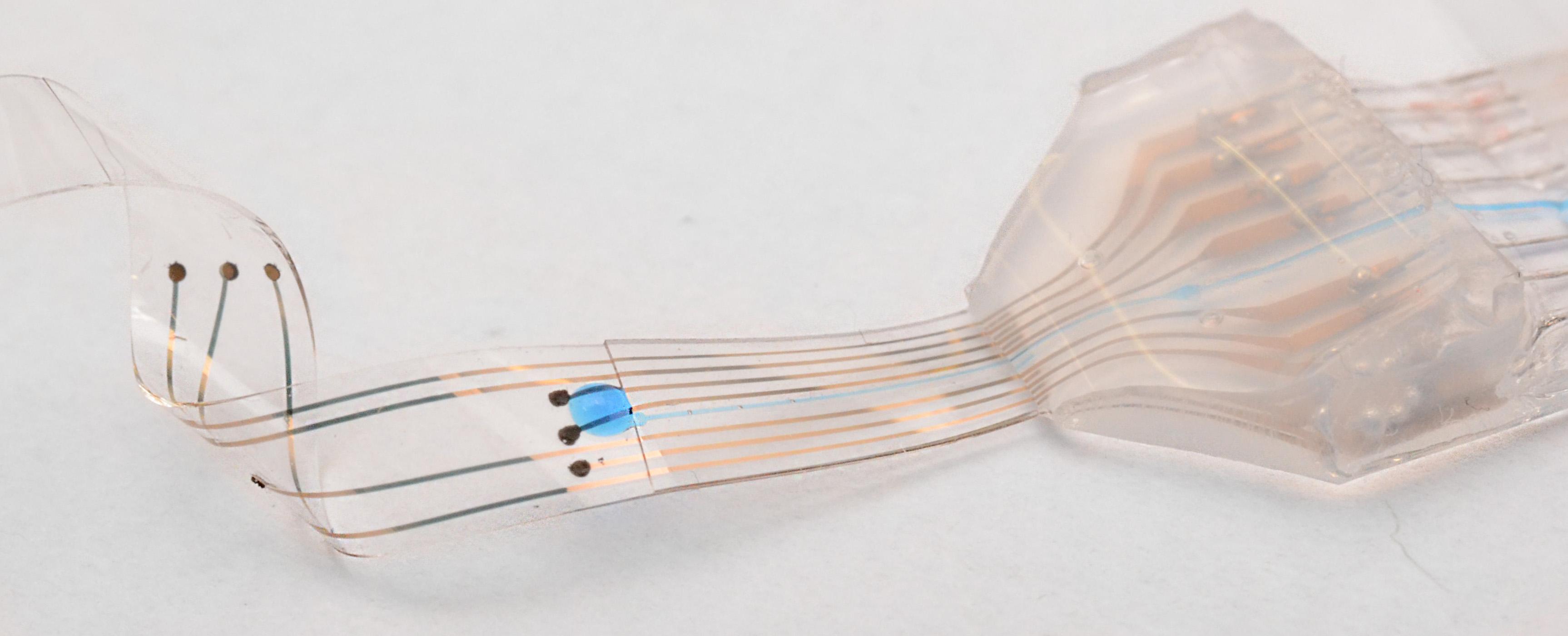
New research shows how inkjet-printing technology can be used to mass-produce electronic circuits made of liquid-metal alloys for “soft robots” and flexible electronics.
Elastic technologies could make possible a new class of pliable robots and stretchable garments that people might wear to interact with computers or for therapeutic purposes. However, new manufacturing techniques must be developed before soft machines become commercially feasible, said Rebecca Kramer, an assistant professor of mechanical engineering at Purdue University.
“We want to create stretchable electronics that might be compatible with soft machines, such as robots that need to squeeze through small spaces, or wearable technologies that aren’t restrictive of motion,” she said. “Conductors made from liquid metal can stretch and deform without breaking.”
A new potential manufacturing approach focuses on harnessing inkjet printing to create devices made of liquid alloys.
“This process now allows us to print flexible and stretchable conductors onto anything, including elastic materials and fabrics,” Kramer said.
A research paper about the method will appear on April 18 [2015] in the journal Advanced Materials. The paper generally introduces the method, called mechanically sintered gallium-indium nanoparticles, and describes research leading up to the project. It was authored by postdoctoral researcher John William Boley, graduate student Edward L. White and Kramer.
A printable ink is made by dispersing the liquid metal in a non-metallic solvent using ultrasound, which breaks up the bulk liquid metal into nanoparticles. This nanoparticle-filled ink is compatible with inkjet printing.
“Liquid metal in its native form is not inkjet-able,” Kramer said. “So what we do is create liquid metal nanoparticles that are small enough to pass through an inkjet nozzle. Sonicating liquid metal in a carrier solvent, such as ethanol, both creates the nanoparticles and disperses them in the solvent. Then we can print the ink onto any substrate. The ethanol evaporates away so we are just left with liquid metal nanoparticles on a surface.”
After printing, the nanoparticles must be rejoined by applying light pressure, which renders the material conductive. This step is necessary because the liquid-metal nanoparticles are initially coated with oxidized gallium, which acts as a skin that prevents electrical conductivity.
“But it’s a fragile skin, so when you apply pressure it breaks the skin and everything coalesces into one uniform film,” Kramer said. “We can do this either by stamping or by dragging something across the surface, such as the sharp edge of a silicon tip.”
The approach makes it possible to select which portions to activate depending on particular designs, suggesting that a blank film might be manufactured for a multitude of potential applications.
“We selectively activate what electronics we want to turn on by applying pressure to just those areas,” said Kramer, who this year was awarded an Early Career Development award from the National Science Foundation, which supports research to determine how to best develop the liquid-metal ink.
The process could make it possible to rapidly mass-produce large quantities of the film.
Future research will explore how the interaction between the ink and the surface being printed on might be conducive to the production of specific types of devices.
“For example, how do the nanoparticles orient themselves on hydrophobic versus hydrophilic surfaces? How can we formulate the ink and exploit its interaction with a surface to enable self-assembly of the particles?” she said.
The researchers also will study and model how individual particles rupture when pressure is applied, providing information that could allow the manufacture of ultrathin traces and new types of sensors.
Here’s a link to and a citation for the paper,
Nanoparticles: Mechanically Sintered Gallium–Indium Nanoparticles by John William Boley, Edward L. White and Rebecca K. Kramer. Advanced Materials Volume 27, Issue 14, page 2270, April 8, 2015 DOI: 10.1002/adma.201570094 Article first published online: 7 APR 2015
I have two items about implants and brains and an item about being able to exert remote control of the brain, all of which hint at a cyborg future for at least a few of us.
e-Dura, the spinal column, and the brain
The first item concerns some research, at the École Polytechnique de Lausanne (EPFL) which features flexible electronics. From a March 24, 2015 article by Ben Schiller for Fast Company (Note: Links have been removed),
Researchers at the Swiss Federal Institute of Technology, in Lausanne, have developed the e-Dura—a tiny skinlike device that attaches directly to damaged spinal cords. By sending out small electrical pulses, it stimulates the cord as if it were receiving signals from the brain, thus allowing movement.
“The purpose of the neuro-prosthesis is to excite the neurons that are on the spinal cord below the site of the injury and activate them, just like if they were receiving information from the brain,” says Stéphanie Lacour, a professor at the institute.
EPFL scientists have managed to get rats walking on their own again using a combination of electrical and chemical stimulation. But applying this method to humans would require multifunctional implants that could be installed for long periods of time on the spinal cord without causing any tissue damage. This is precisely what the teams of professors Stéphanie Lacour and Grégoire Courtine have developed. Their e-Dura implant is designed specifically for implantation on the surface of the brain or spinal cord. The small device closely imitates the mechanical properties of living tissue, and can simultaneously deliver electric impulses and pharmacological substances. The risks of rejection and/or damage to the spinal cord have been drastically reduced. An article about the implant will appear in early January [2015] in Science Magazine.
So-called “surface implants” have reached a roadblock; they cannot be applied long term to the spinal cord or brain, beneath the nervous system’s protective envelope, otherwise known as the “dura mater,” because when nerve tissues move or stretch, they rub against these rigid devices. After a while, this repeated friction causes inflammation, scar tissue buildup, and rejection.
Here’s what the implant looks like,
Courtesy: EPFL
The press release describes how the implant is placed (Note: A link has been removed),
Flexible and stretchy, the implant developed at EPFL is placed beneath the dura mater, directly onto the spinal cord. Its elasticity and its potential for deformation are almost identical to the living tissue surrounding it. This reduces friction and inflammation to a minimum. When implanted into rats, the e-Dura prototype caused neither damage nor rejection, even after two months. More rigid traditional implants would have caused significant nerve tissue damage during this period of time.
The researchers tested the device prototype by applying their rehabilitation protocol — which combines electrical and chemical stimulation – to paralyzed rats. Not only did the implant prove its biocompatibility, but it also did its job perfectly, allowing the rats to regain the ability to walk on their own again after a few weeks of training.
“Our e-Dura implant can remain for a long period of time on the spinal cord or the cortex, precisely because it has the same mechanical properties as the dura mater itself. This opens up new therapeutic possibilities for patients suffering from neurological trauma or disorders, particularly individuals who have become paralyzed following spinal cord injury,” explains Lacour, co-author of the paper, and holder of EPFL’s Bertarelli Chair in Neuroprosthetic Technology.
The press release goes on to describe the engineering achievements,
Developing the e-Dura implant was quite a feat of engineering. As flexible and stretchable as living tissue, it nonetheless includes electronic elements that stimulate the spinal cord at the point of injury. The silicon substrate is covered with cracked gold electric conducting tracks that can be pulled and stretched. The electrodes are made of an innovative composite of silicon and platinum microbeads. They can be deformed in any direction, while still ensuring optimal electrical conductivity. Finally, a fluidic microchannel enables the delivery of pharmacological substances – neurotransmitters in this case – that will reanimate the nerve cells beneath the injured tissue.
The implant can also be used to monitor electrical impulses from the brain in real time. When they did this, the scientists were able to extract with precision the animal’s motor intention before it was translated into movement.
“It’s the first neuronal surface implant designed from the start for long-term application. In order to build it, we had to combine expertise from a considerable number of areas,” explains Courtine, co-author and holder of EPFL’s IRP Chair in Spinal Cord Repair. “These include materials science, electronics, neuroscience, medicine, and algorithm programming. I don’t think there are many places in the world where one finds the level of interdisciplinary cooperation that exists in our Center for Neuroprosthetics.”
For the time being, the e-Dura implant has been primarily tested in cases of spinal cord injury in paralyzed rats. But the potential for applying these surface implants is huge – for example in epilepsy, Parkinson’s disease and pain management. The scientists are planning to move towards clinical trials in humans, and to develop their prototype in preparation for commercialization.
EPFL has provided a video of researcher Stéphanie Lacour describing e-Dura and expressing hopes for its commercialization,
Here’s a link to and a citation for the paper,
Electronic dura mater for long-term multimodal neural interfaces by Ivan R. Minev, Pavel Musienko, Arthur Hirsch, Quentin Barraud, Nikolaus Wenger, Eduardo Martin Moraud, Jérôme Gandar, Marco Capogrosso, Tomislav Milekovic, Léonie Asboth, Rafael Fajardo Torres, Nicolas Vachicouras, Qihan Liu, Natalia Pavlova, Simone Duis, Alexandre Larmagnac, Janos Vörös, Silvestro Micera, Zhigang Suo, Grégoire Courtine, Stéphanie P. Lacour. Science 9 January 2015: Vol. 347 no. 6218 pp. 159-163 DOI: 10.1126/science.1260318
This paper is behind a paywall.
Carbon nanotube fibres could connect to the brain
Researchers at Rice University (Texas, US) are excited about the possibilities that carbon nanotube fibres offer in the field of implantable electronics for the brain. From a March 25, 2015 news item on Nanowerk,
Carbon nanotube fibers invented at Rice University may provide the best way to communicate directly with the brain.
The fibers have proven superior to metal electrodes for deep brain stimulation and to read signals from a neuronal network. Because they provide a two-way connection, they show promise for treating patients with neurological disorders while monitoring the real-time response of neural circuits in areas that control movement, mood and bodily functions.
New experiments at Rice demonstrated the biocompatible fibers are ideal candidates for small, safe electrodes that interact with the brain’s neuronal system, according to the researchers. They could replace much larger electrodes currently used in devices for deep brain stimulation therapies in Parkinson’s disease patients.
They may also advance technologies to restore sensory or motor functions and brain-machine interfaces as well as deep brain stimulation therapies for other neurological disorders, including dystonia and depression, the researchers wrote.
The fibers created by the Rice lab of chemist and chemical engineer Matteo Pasquali consist of bundles of long nanotubes originally intended for aerospace applications where strength, weight and conductivity are paramount.
The individual nanotubes measure only a few nanometers across, but when millions are bundled in a process called wet spinning, they become thread-like fibers about a quarter the width of a human hair.
“We developed these fibers as high-strength, high-conductivity materials,” Pasquali said. “Yet, once we had them in our hand, we realized that they had an unexpected property: They are really soft, much like a thread of silk. Their unique combination of strength, conductivity and softness makes them ideal for interfacing with the electrical function of the human body.”
The simultaneous arrival in 2012 of Caleb Kemere, a Rice assistant professor who brought expertise in animal models of Parkinson’s disease, and lead author Flavia Vitale, a research scientist in Pasquali’s lab with degrees in chemical and biomedical engineering, prompted the investigation.
“The brain is basically the consistency of pudding and doesn’t interact well with stiff metal electrodes,” Kemere said. “The dream is to have electrodes with the same consistency, and that’s why we’re really excited about these flexible carbon nanotube fibers and their long-term biocompatibility.”
Weeks-long tests on cells and then in rats with Parkinson’s symptoms proved the fibers are stable and as efficient as commercial platinum electrodes at only a fraction of the size. The soft fibers caused little inflammation, which helped maintain strong electrical connections to neurons by preventing the body’s defenses from scarring and encapsulating the site of the injury.
The highly conductive carbon nanotube fibers also show much more favorable impedance – the quality of the electrical connection — than state-of-the-art metal electrodes, making for better contact at lower voltages over long periods, Kemere said.
The working end of the fiber is the exposed tip, which is about the width of a neuron. The rest is encased with a three-micron layer of a flexible, biocompatible polymer with excellent insulating properties.
The challenge is in placing the tips. “That’s really just a matter of having a brain atlas, and during the experiment adjusting the electrodes very delicately and putting them into the right place,” said Kemere, whose lab studies ways to connect signal-processing systems and the brain’s memory and cognitive centers.
Doctors who implant deep brain stimulation devices start with a recording probe able to “listen” to neurons that emit characteristic signals depending on their functions, Kemere said. Once a surgeon finds the right spot, the probe is removed and the stimulating electrode gently inserted. Rice carbon nanotube fibers that send and receive signals would simplify implantation, Vitale said.
The fibers could lead to self-regulating therapeutic devices for Parkinson’s and other patients. Current devices include an implant that sends electrical signals to the brain to calm the tremors that afflict Parkinson’s patients.
“But our technology enables the ability to record while stimulating,” Vitale said. “Current electrodes can only stimulate tissue. They’re too big to detect any spiking activity, so basically the clinical devices send continuous pulses regardless of the response of the brain.”
Kemere foresees a closed-loop system that can read neuronal signals and adapt stimulation therapy in real time. He anticipates building a device with many electrodes that can be addressed individually to gain fine control over stimulation and monitoring from a small, implantable device.
“Interestingly, conductivity is not the most important electrical property of the nanotube fibers,” Pasquali said. “These fibers are intrinsically porous and extremely stable, which are both great advantages over metal electrodes for sensing electrochemical signals and maintaining performance over long periods of time.”
The paper is open access provided you register on the website.
Remote control for stimulation of the brain
Mo Costandi, neuroscientist and freelance science writer, has written a March 24, 2015 post for the Guardian science blog network focusing on neuronal remote control,
Two teams of scientists have developed new ways of stimulating neurons with nanoparticles, allowing them to activate brain cells remotely using light or magnetic fields. The new methods are quicker and far less invasive than other hi-tech methods available, so could be more suitable for potential new treatments for human diseases.
Researchers have various methods for manipulating brain cell activity, arguably the most powerful being optogenetics, which enables them to switch specific brain cells on or off with unprecedented precision, and simultaneously record their behaviour, using pulses of light.
This is very useful for probing neural circuits and behaviour, but involves first creating genetically engineered mice with light-sensitive neurons, and then inserting the optical fibres that deliver light into the brain, so there are major technical and ethical barriers to its use in humans.
Nanomedicine could get around this. Francisco Bezanilla of the University of Chicago and his colleagues knew that gold nanoparticles can absorb light and convert it into heat, and several years ago they discovered that infrared light can make neurons fire nervous impulses by heating up their cell membranes.
…
Polina Anikeeva’s team at the Massachusetts Institute of Technology adopted a slightly different approach, using spherical iron oxide particles that give off heat when exposed to an alternating magnetic field.
…
Although still in the experimental stages, research like this may eventually allow for wireless and minimally invasive deep brain stimulation of the human brain. Bezanilla’s group aim to apply their method to develop treatments for macular degeneration and other conditions that kill off light-sensitive cells in the retina. This would involve injecting nanoparticles into the eye so that they bind to other retinal cells, allowing natural light to excite them into firing impulses to the optic nerve.
Costandi’s article is intended for an audience that either understands the science or can deal with the uncertainty of not understanding absolutely everything. Provided you fall into either of those categories, the article is well written and it provides links and citations to the papers for both research teams being featured.
Taken together, the research at EPFL, Rice University, University of Chicago, and Massachusetts Institute of Technology provides a clue as to how much money and intellectual power is being directed at the brain.
A March 5, 2015 news item on Azonano highlights work on flexible, transparent electronics designed to adhere to your skin,
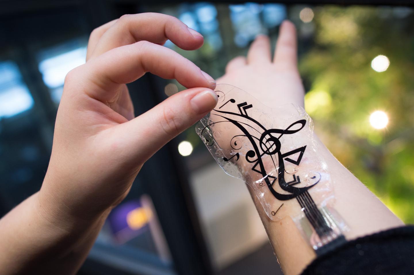
Someone wearing a smartwatch can look at a calendar or receive e-mails without having to reach further than their wrist. However, the interaction area offered by the watch face is both fixed and small, making it difficult to actually hit individual buttons with adequate precision. A method currently being developed by a team of computer scientists from Saarbrücken in collaboration with researchers from Carnegie Mellon University in the USA may provide a solution to this problem. They have developed touch-sensitive stickers made from flexible silicone and electrically conducting sensors that can be worn on the skin.
Here’s what the sticker looks like,
Caption: The stickers are skin-friendly and are attached to the skin with a biocompatible, medical-grade adhesive. Credit: Oliver Dietze Courtesy: Saarland University
… The stickers can act as an input space that receives and executes commands and thus controls mobile devices. Depending on the type of skin sticker used, applying pressure to the sticker could, for example, answer an incoming call or adjust the volume of a music player. ‘The stickers allow us to enlarge the input space accessible to the user as they can be attached practically anywhere on the body,’ explains Martin Weigel, a PhD student in the team led by Jürgen Steimle at the Cluster of Excellence at Saarland University. The ‘iSkin’ approach enables the human body to become more closely connected to technology. [emphasis mine]
Users can also design their iSkin patches on a computer beforehand to suit their individual tastes. ‘A simple graphics program is all you need,’ says Weigel. One sticker, for instance, is based on musical notation, another is circular in shape like an LP. The silicone used to fabricate the sensor patches makes them flexible and stretchable. ‘This makes them easier to use in an everyday environment. The music player can simply be rolled up and put in a pocket,’ explains Jürgen Steimle, who heads the ‘Embodied Interaction Group’ in which Weigel is doing his research. ‘They are also skin-friendly, as they are attached to the skin with a biocompatible, medical-grade adhesive. Users can therefore decide where they want to position the sensor patch and how long they want to wear it.’
In addition to controlling music or phone calls, the iSkin technology could be used for many other applications. For example, a keyboard sticker could be used to type and send messages. Currently the sensor stickers are connected via cable to a computer system. According to Steimle, in-built microchips may in future allow the skin-worn sensor patches to communicate wirelessly with other mobile devices.
The publication about ‘iSkin’ won the ‘Best Paper Award’ at the SIGCHI conference, which ranks among the most important conferences within the research area of human computer interaction. The researchers will present their project at the SIGCHI conference in April [2015] in Seoul, Korea, and beforehand at the computer expo Cebit, which takes place from the 16th until the 20th of March [2015] in Hannover (hall 9, booth E13).
Hopefully, you’ll have a chance to catch researchers’ presentation at the SIGCHI or Cebit events.
That quote about enabling “the human body to become more closely connected to technology” reminds me of a tag (machine/flesh) I created to categorize research of this nature. I explained the idea being explored in a May 9, 2012 posting titled: Everything becomes part machine,
Machine/flesh. That’s what I’ve taken to calling this process of integrating machinery into our and, as I newly realized, other animals’ flesh.
It seems there could be a new member of the flexible electronics materials community, silver nanowires, according to a Jan. 23, 2015 news item on ScienceDaily,
Wth its high electrical conductivity and optical transparency, indium tin oxide is one of the most widely used materials for touchscreens, plasma displays, and flexible electronics. But its rapidly escalating price has forced the electronics industry to search for other alternatives.
One potential and more cost-effective alternative is a film made with silver nanowires–wires so extremely thin that they are one-dimensional–embedded in flexible polymers. Like indium tin oxide, this material is transparent and conductive. But development has stalled because scientists lack a fundamental understanding of its mechanical properties.
… Horacio Espinosa, the James N. and Nancy J. Farley Professor in Manufacturing and Entrepreneurship at Northwestern University’s McCormick School of Engineering, has led research that expands the understanding of silver nanowires’ behavior in electronics.
Espinosa and his team investigated the material’s cyclic loading, which is an important part of fatigue analysis because it shows how the material reacts to fluctuating loads of stress.
“Cyclic loading is an important material behavior that must be investigated for realizing the potential applications of using silver nanowires in electronics,” Espinosa said. “Knowledge of such behavior allows designers to understand how these conductive films fail and how to improve their durability.”
By varying the tension on silver nanowires thinner than 120 nanometers and monitoring their deformation with electron microscopy, the research team characterized the cyclic mechanical behavior. They found that permanent deformation was partially recoverable in the studied nanowires, meaning that some of the material’s defects actually self-healed and disappeared upon cyclic loading. These results indicate that silver nanowires could potentially withstand strong cyclic loads for long periods of time, which is a key attribute needed for flexible electronics.
“These silver nanowires show mechanical properties that are quite unexpected,” Espinosa said. “We had to develop new experimental techniques to be able to measure this novel material property.”
The findings were recently featured on the cover of the journal Nano Letters. Other Northwestern coauthors on the paper are Rodrigo Bernal, a recently graduated PhD student in Espinosa’s lab, and Jiaxing Huang, associate professor of materials science and engineering in McCormick.
“The next step is to understand how this recovery influences the behavior of these materials when they are flexed millions of times,” said Bernal, first author of the paper.
This particular version of the paper is behind a paywall. However, access to the paper is possible although I make no claims as to which version it is or whether it will continue to be freely accessible.
Korean scientists are trying to make the process of creating flexible electronics easier according to a Nov. 25, 2014 news item on ScienceDaily,
Flexible electronics have been touted as the next generation in electronics in various areas, ranging from consumer electronics to bio-integrated medical devices. In spite of their merits, insufficient performance of organic materials arising from inherent material properties and processing limitations in scalability have posed big challenges to developing all-in-one flexible electronics systems in which display, processor, memory, and energy devices are integrated. The high temperature processes, essential for high performance electronic devices, have severely restricted the development of flexible electronics because of the fundamental thermal instabilities of polymer materials.
A research team headed by Professor Keon Jae Lee of the Department of Materials Science and Engineering at KAIST provides an easier methodology to realize high performance flexible electronics by using the Inorganic-based Laser Lift-off (ILLO).
The process is described in a Nov. 26, 2014 KAIST news release on ResearchSEA, which originated the news item (despite the confusion of the date, probably due to timezone differentials), provides more detail about the technique for ILLO,
The ILLO process involves depositing a laser-reactive exfoliation layer on rigid substrates, and then fabricating ultrathin inorganic electronic devices, e.g., high density crossbar memristive memory on top of the exfoliation layer. By laser irradiation through the back of the substrate, only the ultrathin inorganic device layers are exfoliated from the substrate as a result of the reaction between laser and exfoliation layer, and then subsequently transferred onto any kind of receiver substrate such as plastic, paper, and even fabric.
This ILLO process can enable not only nanoscale processes for high density flexible devices but also the high temperature process that was previously difficult to achieve on plastic substrates. The transferred device successfully demonstrates fully-functional random access memory operation on flexible substrates even under severe bending.
Professor Lee said, “By selecting an optimized set of inorganic exfoliation layer and substrate, a nanoscale process at a high temperature of over 1000 °C can be utilized for high performance flexible electronics. The ILLO process can be applied to diverse flexible electronics, such as driving circuits for displays and inorganic-based energy devices such as battery, solar cell, and self-powered devices that require high temperature processes.”
Here’s a link to and a citation for the research paper,
Northwestern University’s Yonggang Huang and the University of Illinois’ John A. Rogers are the first to demonstrate a stretchable lithium-ion battery — a flexible device capable of powering their innovative stretchable electronics.
No longer needing to be connected by a cord to an electrical outlet, the stretchable electronic devices now could be used anywhere, including inside the human body. The implantable electronics could monitor anything from brain waves to heart activity, succeeding where flat, rigid batteries would fail.
Huang and Rogers have demonstrated a battery that continues to work — powering a commercial light-emitting diode (LED) — even when stretched, folded, twisted and mounted on a human elbow. The battery can work for eight to nine hours before it needs recharging, which can be done wirelessly.
The researchers at Northwestern have produced a video where they demonstrate the battery’s ‘stretchability’,
“We start with a lot of battery components side by side in a very small space, and we connect them with tightly packed, long wavy lines,” said Huang, a corresponding author of the paper. “These wires provide the flexibility. When we stretch the battery, the wavy interconnecting lines unfurl, much like yarn unspooling. And we can stretch the device a great deal and still have a working battery.”
…
The power and voltage of the stretchable battery are similar to a conventional lithium-ion battery of the same size, but the flexible battery can stretch up to 300 percent of its original size and still function.
…
Huang and Rogers have been working together for the last six years on stretchable electronics, and designing a cordless power supply has been a major challenge. Now they have solved the problem with their clever “space filling technique,” which delivers a small, high-powered battery.
For their stretchable electronic circuits, the two developed “pop-up” technology that allows circuits to bend, stretch and twist. They created an array of tiny circuit elements connected by metal wire “pop-up bridges.” When the array is stretched, the wires — not the rigid circuits — pop up.
This approach works for circuits but not for a stretchable battery. A lot of space is needed in between components for the “pop-up” interconnect to work. Circuits can be spaced out enough in an array, but battery components must be packed tightly to produce a powerful but small battery. There is not enough space between battery components for the “pop-up” technology to work.
Huang’s design solution is to use metal wire interconnects that are long, wavy lines, filling the small space between battery components. (The power travels through the interconnects.)
The unique mechanism is a “spring within a spring”: The line connecting the components is a large “S” shape and within that “S” are many smaller “S’s.” When the battery is stretched, the large “S” first stretches out and disappears, leaving a line of small squiggles. The stretching continues, with the small squiggles disappearing as the interconnect between electrodes becomes taut.
“We call this ordered unraveling,” Huang said. “And this is how we can produce a battery that stretches up to 300 percent of its original size.”
The stretching process is reversible, and the battery can be recharged wirelessly. The battery’s design allows for the integration of stretchable, inductive coils to enable charging through an external source but without the need for a physical connection.
Huang, Rogers and their teams found the battery capable of 20 cycles of recharging with little loss in capacity. The system they report in the paper consists of a square array of 100 electrode disks, electrically connected in parallel.
I’d like to see this battery actually powering a device even though the stretching is quite alluring in its way. For those who are interested here’s a citation and a link to the research paper,
Stretchable batteries with self-similar serpentine interconnects and integrated wireless recharging systems by Sheng Xu, Yihui Zhang, Jiung Cho, Juhwan Lee, Xian Huang, Lin Jia, Jonathan A. Fan, Yewang Su, Jessica Su, Huigang Zhang, Huanyu Cheng, Bingwei Lu, Cunjiang Yu, Chi Chuang, Tae-il Kim, Taeseup Song, Kazuyo Shigeta, Sen Kang, Canan Dagdeviren, Ivan Petrov et al. Nature Communications 4, Article number: 1543 doi: 10.1038/ncomms2553 Published 26 February 2013
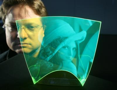
This shows the world’s first flexible and completely transparent image sensor. The plastic film is coated with fluorescent particles. Credit: Optics Express.
Stunning isn’t it? The work is from researchers at the Johannes Kepler University Linz in Austria and is featured in an article being published in Optics Express. From the Feb. 20, 2013 news release about the Optics Express article on EurekAlert,
Digital cameras, medical scanners, and other imaging technologies have advanced considerably during the past decade. Continuing this pace of innovation, an Austrian research team has developed an entirely new way of capturing images based on a flat, flexible, transparent, and potentially disposable polymer sheet. The team describes their new device and its possible applications in a paper published today in the Optical Society’s (OSA) open-access journal Optics Express.
The new imager, which resembles a flexible plastic film, uses fluorescent particles to capture incoming light and channel a portion of it to an array of sensors framing the sheet. With no electronics or internal components, the imager’s elegant design makes it ideal for a new breed of imaging technologies, including user interface devices that can respond not to a touch, but merely to a simple gesture.
The news release goes on to describe the technology,
The sensor is based on a polymer film known as a luminescent concentrator (LC), which is suffused with tiny fluorescent particles that absorb a very specific wavelength (blue light for example) and then reemit it at a longer wavelength (green light for example). Some of the reemitted fluorescent light is scattered out of the imager, but a portion of it travels throughout the interior of the film to the outer edges, where arrays of optical sensors (similar to 1-D pinhole cameras) capture the light. A computer then combines the signals to create a gray-scale image. “With fluorescence, a portion of the light that is reemitted actually stays inside the film,” says Bimber. [Oliver Bimber of the Johannes Kepler University Linz in Austria, co-author of the Optics Express paper] “This is the basic principle of our sensor.”
For the luminescent concentrator to work as an imager, Bimber and his colleagues had to determine precisely where light was falling across the entire surface of the film. This was the major technical challenge because the polymer sheet cannot be divided into individual pixels like the CCD camera inside a smartphone. Instead, fluorescent light from all points across its surface travels to all the edge sensors. Calculating where each bit of light entered the imager would be like determining where along a subway line a passenger got on after the train reached its final destination and all the passengers exited at once.
The solution came from the phenomenon of light attenuation, or dimming, as it travels through the polymer. The longer it travels, the dimmer it becomes. So by measuring the relative brightness of light reaching the sensor array, it was possible to calculate where the light entered the film. This same principle has already been employed in an input device that tracks the location of a single laser point on a screen.
The researchers were able to scale up this basic principle by measuring how much light arrives from every direction at each position on the image sensor at the film’s edge. They could then reconstruct the image by using a technique similar to X-ray computed tomography, more commonly known as a CT scan.
“In CT technology, it’s impossible to reconstruct an image from a single measurement of X-ray attenuation along one scanning direction alone,” says Bimber. “With a multiple of these measurements taken at different positions and directions, however, this becomes possible. Our system works in the same way, but where CT uses X-rays, our technique uses visible light.”
Currently, the resolution from this image sensor is low (32×32 pixels with the first prototypes). The main reason for this is the limited signal-to-noise ratio of the low-cost photodiodes being used. The researchers are planning better prototypes that cool the photodiodes to achieve a higher signal-to-noise ratio.
By applying advanced sampling techniques, the researchers can already enhance the resolution by reconstructing multiple images at different positions on the film. These positions differ by less than a single pixel (as determined by the final image, not the polymer itself). By having multiple of these slightly different images reconstructed, it’s possible to create a higher resolution image. “This does not require better photodiodes,” notes Bimber, “and does not make the sensor significantly slower. The more images we combine, the higher the final resolution is, up to a certain limit.”
The researchers discuss applications,
The main application the researchers envision for this new technology is in touch-free, transparent user interfaces that could seamlessly overlay a television or other display technology. This would give computer operators or video-game players full gesture control without the need for cameras or other external motion-tracking devices. The polymer sheet could also be wrapped around objects to provide them with sensor capabilities. Since the material is transparent, it’s also possible to use multiple layers that each fluoresce at different wavelengths to capture color images.
The researchers also are considering attaching their new sensor in front of a regular, high-resolution CCD sensor. This would allow recording of two images at the same time at two different exposures. “Combining both would give us a high-resolution image with less overexposed or underexposed regions if scenes with a high dynamic range or contrast are captured,” Bimber speculates. He also notes that the polymer sheet portion of the device is relatively inexpensive and therefore disposable. “I think there are many applications for this sensor that we are not yet aware of,” he concludes.
Here’s a citation and a link,
“Towards a transparent, flexible, scalable and disposable image sensor using thin-film luminescent concentrators,” A. Koppelhuber and O. Bimber, Optics Express, Vol. 21, Issue 4, pp. 4796-4810 (2013) (link: http://www.opticsinfobase.org/oe/abstract.cfm?uri=oe-21-4-4796).
Roel Vertegaal at Queen’s University (Ontario, Canada) has released a ‘paper’ tablet. Like the bendable, flexible ‘paper’ phone he presented at the CHI 2011 meeting in Vancouver, Canada (my May 12, 2011 posting), this tablet offers some intriguing possibilities but is tethered. The Jan. 9, 2013 news item on phys.org provides more information about the new ‘paper’ device (Note: Links have been removed),
Watch out tablet lovers – a flexible paper computer developed at Queen’s University in collaboration with Plastic Logic and Intel Labs will revolutionize the way people work with tablets and computers.
The PaperTab tablet looks and feels just like a sheet of paper. However, it is fully interactive with a flexible, high-resolution 10.7-inch plastic display developed by Plastic Logic and a flexible touchscreen. It is powered by the second generation I5 Core processor developed by Intel.
Vertegaal and his team have produced a video demonstrating their ‘paper’ tablet/computer:
“Using several PaperTabs makes it much easier to work with multiple documents,” says Roel Vertegaal, Director of Queen’s University’s Human Media Lab. “Within five to ten years, most computers, from ultra-notebooks to tablets, will look and feel just like these sheets of printed color paper.”
“We are actively exploring disruptive user experiences. The ‘PaperTab’ project, developed by the Human Media Lab at Queen’s University and Plastic Logic, demonstrates novel interactions powered by Intel processors that could potentially delight tablet users in the future,” says Intel’s Experience Design Lead Research Scientist, Ryan Brotman.
PaperTab’s intuitive interface allows users to create a larger drawing or display surface by placing two or more PaperTabs side by side. PaperTab emulates the natural handling of multiple sheets of paper. It can file and display thousands of paper documents, replacing the need for a computer monitor and stacks of papers or printouts.
Unlike traditional tablets, PaperTabs keep track of their location relative to each other, and to the user, providing a seamless experience across all apps, as if they were physical computer windows.
“Plastic Logic’s flexible plastic displays allow a natural human interaction with electronic paper, being lighter, thinner and more robust compared with today’s standard glass-based displays. This is just one example of the innovative revolutionary design approaches enabled by flexible displays,” explains Indro Mukerjee, CEO of Plastic Logic.
The partners are saying that ‘paper’ tablets may be on the market in foreseeable future according to Emma Wollacott’s Jan. 8, 2013 article for TG Daily,
The bendy tablet has been coming for quite a while now, but a version to be shown off today at CES [Consumer Electronics Show] could be ready for the market within three years, say its creators.
The CONTEST (COllaborative Network for Training in Electronic Skin TechnologyCOllaborative Network for Training in Electronic Skin Technology) project was launched today in Italy. According to the Aug. 21, 2012 news item on Nanowerk,
“Flexible electronics” is one of the most significant challenges in the field of future electronics. The possibility of realizing flexible and bendable electronic circuits, that can be rolled up, twisted or inserted in films around objects, would introduce a range of infinite applications in multiple fields, including healthcare, robotics and energy.
In this area, the Fondazione Bruno Kessler of Trento will coordinate the CONTEST project (COllaborative Network for Training in Electronic Skin Technology), an Initial Training Network (ITN) Marie Curie project funded by the European Commission involving European research, academic and business players. These include seven full partners (Fondazione Bruno Kessler, Italy; ST Microelectronics, Italy; Technical University Munich, Germany; Fraunhofer EMFT, Germany; University College London, UK; Imperial College London, UK; and Shadow Robotics Company, UK) and two associate partners (University of Cambridge, UK, and University of Tokyo, Japan).
The CONTEST project page at the Fondazione Bruno Kessler website offers more details,
At the heart of the CONTEST programme lies the multidisciplinary research training of young researchers. The CONTEST network will recruit twelve excellent Early-Stage Researchers (e.g. PhD students) and two Experienced Researchers (e.g. Post-Doc fellows). Information for submitting applications is available at the project’s website: http://www.contest-itn.eu/.
CONTEST activities will be coordinated by Ravinder S. Dahiya, researcher at the Bio-MEMS Unit (BIO-Micro-Electro-Mechanical-Systems) of the Center for Materials and Microsystems (Fondazione Bruno Kessler) and by Leandro Lorenzelli, head of the Bio-MEMS Unit.
“The disruptive flexible electronics technology – says Ravinder S. Dahiya – will create change and improve the electronic market landscape and usher in a new revolution in multifunctional electronics. It will transform to an unprecedented degree our view of electronics and how we, as a society, interact with intelligent and responsive systems.”
“The investigation, in a very multidisciplinary framework, of technological approaches for thin flexible components – explains Leandro Lorenzelli – will generate new paradigms and concepts for microelectronic devices and systems with new functionalities tailored to the needs of a wide range of applications including robotics, biomedical instrumentations and smart cities.”
Here’s more about the 12 researchers they’re recruiting, excerpted from the Job Openings page on the CONTEST project website (Note: I have removed some links),
We have been awarded a large interdisciplinary project on electronic skin and applications, called CONTEST (COllaborative Network for Training in Electronic Skin Technology). We are therefore looking for 12 excellent Early-Stage Researchers (e.g. PhD students) and 2 Experienced Researchers (e.g. Post-Doc), associated to:
Fondazione Bruno Kessler, Trento, Italy (2 Early-Stage Researcher positions on silicon based flexible sensors (e.g. touch sensors), electronic circuits and 1 Experienced Researcher position on system integration) …,
ST Microelectronics, Catania, Italy (2 Early-Stage Researcher positions on chemical/physical sensors on flexible substrates, and metal patterned substrates for integrating flexible sensing elements)…,
Technical University Munich, Germany (3 Early-Stage Researcher positions on organic semiconductor based electronics devices and circuits, modeling of flexible devices and sensors … , and artificial skin in humanoids…,
Fraunhofer EMFT, Munich, Germany (1 Early-Stage Researcher position on assembly on film substrates and foil integration as well as 1 Experienced Researcher position on reliability and ESD issues of components during flex integration) … ,
University College London, UK (2 Early-Stage Researcher positions on organic semiconductor based interconnects, solutions processed sensors, alternative on-skin energy schemes, patterning of e-skin and stretchable interconnects using blends of graphene in polymeric materials …
Imperial College London, UK (1 Early-Stage Researcher position on human sensori-motor control and robotics) …, and
Shadow Robotics Company, UK (1 Early-Stage Researcher position on biorobotics and mechatronics) ….
Mobility rules apply to all these positions. Researchers can be of any nationality. They are required to undertake trans-national mobility (i.e. move from one country to another) when taking up their appointment. One general rule applies to the appointment of researchers: At the time of recruitment by the host organization, researchers must not have resided or carried out their main activity (work, studies, etc.) in the country of their host organization (i.e. recruiting institute) for more than 12 months in the 3 years immediately prior to the reference date. Short stays such as holidays and/or compulsory national service are not taken into account.
Good luck to all who apply! Priority will be given to applications received by Sept. 30, 2012.
I don’t think you actually need to shake but you do need to bake your cotton t-shirt, albeit in a special way, to create a wearable battery or so the University of South Carolina’s Xiaodong Li says. Excerpted from the June 29, 2012 news item on Nanowerk,
Over the years, the telephone has gone mobile, from the house to the car to the pocket. The University of South Carolina’s Xiaodong Li envisions even further integration of the cell phone – and just about every electronic gadget, for that matter – into our lives.
…
“We wear fabric every day,” said Li, a professor of mechanical engineering at USC. “One day our cotton T-shirts could have more functions; for example, a flexible energy storage device that could charge your cell phone or your iPad.”
Li is helping make the vision a reality. He and post-doctoral associate Lihong Bao have just reported in the journal Advanced Materials (“Towards Textile Storage from Cotton T-Shirts”) how to turn the material in a cotton T-shirt into a source of electrical power.
Starting with a T-shirt from a local discount store, Li’s team soaked it in a solution of fluoride, dried it and baked it at high temperature. They excluded oxygen in the oven to prevent the material from charring or simply combusting.
The surfaces of the resulting fibers in the fabric were shown by infrared spectroscopy to have been converted from cellulose to activated carbon. Yet the material retained flexibility; it could be folded without breaking.
“We will soon see roll-up cell phones and laptop computers on the market,” Li said. “But a flexible energy storage device is needed to make this possible.”
The once-cotton T-shirt proved to be a repository for electricity. By using small swatches of the fabric as an electrode, the researchers showed that the flexible material, which Li’s team terms activated carbon textile, acts as a capacitor. Capacitors are components of nearly every electronic device on the market, and they have the ability to store electrical charge.
Here’s what makes the approach different; it’s ‘green’ according to Powell’s news release,
Li is particularly pleased to have improved on the means by which activated carbon fibers are usually obtained. “Previous methods used oil or environmentally unfriendly chemicals as starting materials,” he said. “Those processes are complicated and produce harmful side products. Our method is a very inexpensive, green process.”
Somehow I’ve always seen ‘wearable batteries and/or electronics’ as opportunities for electrocution but I seem to be alone with this fear as there’s never any discussion about the safety issues might arise.
ETA July 3, 2012: Dexter Johnson in his June 29, 2012 posting on Nanoclast (a blog on the IEEE [Institute of Electrical and Electronics Engineers] website) notes that the simplicity of Li’s process may be specially exciting,
While Li makes mention of the environmentally friendly chemicals used to impart this capability to a t-shirt, it is perhaps the simplicity of the process that will likely be the most intriguing aspect to manufacturers.