The new nanoparticle comes courtesy of an international collaboration (US, China, Sweden, and Russia. A Nov. 10, 2015 University of Buffalo news release (also on EurekAlert) by Charlotte Hu describes the particle and its properties,
A new, onion-like nanoparticle could open new frontiers in biomaging, solar energy harvesting and light-based security techniques.
The particle’s innovation lies in its layers: a coating of organic dye, a neodymium-containing shell, and a core that incorporates ytterbium and thulium. Together, these strata convert invisible near-infrared light to higher energy blue and UV light with record-high efficiency, a trick that could improve the performance of technologies ranging from deep-tissue imaging and light-induced therapy to security inks used for printing money.
Here’s an artist’s representation of the new nanoparticle,
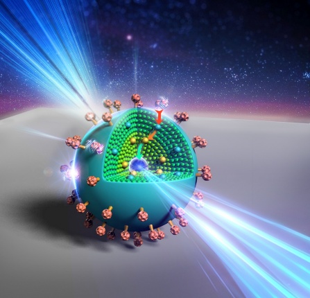
An artist’s rendering shows the layers of a new, onion-like nanoparticle whose specially crafted layers enable it to efficiently convert invisible near-infrared light to higher energy blue and UV light. Credit: Kaiheng Wei Courtesy: University of Buffalo
The news release goes on to describe technology in more detail,
When it comes to bioimaging, near-infrared light could be used to activate the light-emitting nanoparticles deep inside the body, providing high-contrast images of areas of interest. In the realm of security, nanoparticle-infused inks could be incorporated into currency designs; such ink would be invisible to the naked eye, but glow blue when hit by a low-energy laser pulse — a trait very difficult for counterfeiters to reproduce.
“It opens up multiple possibilities for the future,” says Tymish Ohulchanskyy, deputy director of photomedicine and research associate professor at the Institute for Lasers, Photonics, and Biophotonics (ILPB) at the University at Buffalo.
“By creating special layers that help transfer energy efficiently from the surface of the particle to the core, which emits blue and UV light, our design helps overcome some of the long-standing obstacles that previous technologies faced,” says Guanying Chen, professor of chemistry at Harbin Institute of Technology [China] and ILPB research associate professor.
“Our particle is about 100 times more efficient at ‘upconverting’ light than similar nanoparticles created in the past, making it much more practical,” says Jossana Damasco, a UB chemistry PhD student who played a key role in the project.
The research was published online in Nano Letters on Oct. 21 and led by the Institute for Lasers, Photonics, and Biophotonics at UB, and the Harbin Institute of Technology in China, with contributions from the Royal Institute of Technology in Sweden; Tomsk State University in Russia; and the University of Massachusetts Medical School.
The study’s senior author was Paras Prasad, ILPB executive director and SUNY [State University of New York] Distinguished Professor in chemistry, physics, medicine and electrical engineering at UB.
Peeling back the layers
Converting low-energy light to light of higher energies isn’t easy to do. The process involves capturing two or more tiny packets of light called “photons” from a low-energy light source, and combining their energy to form a single, higher-energy photon.
The onionesque nanoparticle performs this task beautifully. Each of its three layers fulfills a unique function:
- The outermost layer is a coating of organic dye. This dye is adept at absorbing photons from low-energy near-infrared light sources. It acts as an “antenna” for the nanoparticle, harvesting light and transferring energy inside, Ohulchanskyy says.
- The next layer is a neodymium-containing shell. This layer acts as a bridge, transferring energy from the dye to the particle’s light-emitting core.
- Inside the light-emitting core, ytterbium and thulium ions work in concert. The ytterbium ions draw energy into the core and pass the energy on to the thulium ions, which have special properties that enable them to absorb the energy of three, four or five photons at once, and then emit a single higher-energy photon of blue and UV light.
So why not just use the core? Why add the dye and neodymium layer at all?
As Ohulchanskyy and Chen explain, the core itself is inefficient in absorbing photons from the outside world. That’s where the dye comes in.
Once you add the dye, the neodymium-containing layer is necessary for transferring energy efficiently from dye to core. Ohulchanskyy uses the analogy of a staircase to explain why this is: When molecules or ions in a material absorb a photon, they enter an “excited” state from which they can transfer energy to other molecules or ions. The most efficient transfer occurs between molecules or ions whose excited states require a similar amount of energy to obtain, but the dye and ytterbium ions have excited states with very different energies. So the team added neodymium — whose excited state is in between that of the dye and thulium’s — to act as a bridge between the two, creating a “staircase” for the energy to travel down to reach emitting thulium ions.
Here’s a link to and a citation for the paper,
Energy-Cascaded Upconversion in an Organic Dye-Sensitized Core/Shell Fluoride Nanocrystal by Guanying Chen, Jossana Damasco, Hailong Qiu, Wei Shao, Tymish Y. Ohulchanskyy, Rashid R. Valiev, Xiang Wu, Gang Han, Yan Wang, Chunhui Yang, Hans Ågren, and Paras N. Prasad. Nano Lett., 2015, 15 (11), pp 7400–7407 DOI: 10.1021/acs.nanolett.5b02830 Publication Date (Web): October 21, 2015
Copyright © 2015 American Chemical Society
This paper is behind a paywall.
Finally, there is a Nov. 11, 2015 article about the research by Jake Wilkinson for Azonano. He provides additional details such as this measurement,
Measuring approximately 50nm in diameter, the new nanoparticle features three differently designed layers. …
*’ayered’ changed to ‘layered’ on Nov. 11, 2015.