Tag Archives: NSF

Embroidering electronics into clothing

Researchers at The Ohio State University are developing embroidered antennas and circuits with 0.1 mm precision—the perfect size to integrate electronic components such as sensors and computer memory devices into clothing. Photo by Jo McCulty, courtesy of The Ohio State University.

Researchers at The Ohio State University are developing embroidered antennas and circuits with 0.1 mm precision—the perfect size to integrate electronic components such as sensors and computer memory devices into clothing. Photo by Jo McCulty, courtesy of The Ohio State University.

An April 13, 2016 news item on Nanowerk describes an advance in the field of wearable electronics,

Researchers who are working to develop wearable electronics have reached a milestone: They are able to embroider circuits into fabric with 0.1 mm precision—the perfect size to integrate electronic components such as sensors and computer memory devices into clothing.

With this advance, the Ohio State University researchers have taken the next step toward the design of functional textiles—clothes that gather, store, or transmit digital information. With further development, the technology could lead to shirts that act as antennas for your smart phone or tablet, workout clothes that monitor your fitness level, sports equipment that monitors athletes’ performance, a bandage that tells your doctor how well the tissue beneath it is healing—or even a flexible fabric cap that senses activity in the brain.

That last item is one that John Volakis, director of the ElectroScience Laboratory at Ohio State, and research scientist Asimina Kiourti are investigating. The idea is to make brain implants, which are under development to treat conditions from epilepsy to addiction, more comfortable by eliminating the need for external wiring on the patient’s body.

An April 13, 2016 Ohio State University news release by Pam Frost Gorder, which originated the news item, expands on the theme (Note: Links have been removed),

“A revolution is happening in the textile industry,” said Volakis, who is also the Roy & Lois Chope Chair Professor of Electrical Engineering at Ohio State. “We believe that functional textiles are an enabling technology for communications and sensing—and one day even medical applications like imaging and health monitoring.”

Recently, he and Kiourti refined their patented fabrication method to create prototype wearables at a fraction of the cost and in half the time as they could only two years ago. With new patents pending, they published the new results in the journal IEEE Antennas and Wireless Propagation Letters.

In Volakis’ lab, the functional textiles, also called “e-textiles,” are created in part on a typical tabletop sewing machine—the kind that fabric artisans and hobbyists might have at home. Like other modern sewing machines, it embroiders thread into fabric automatically based on a pattern loaded via a computer file. The researchers substitute the thread with fine silver metal wires that, once embroidered, feel the same as traditional thread to the touch.

“We started with a technology that is very well known—machine embroidery—and we asked, how can we functionalize embroidered shapes? How do we make them transmit signals at useful frequencies, like for cell phones or health sensors?” Volakis said. “Now, for the first time, we’ve achieved the accuracy of printed metal circuit boards, so our new goal is to take advantage of the precision to incorporate receivers and other electronic components.”

The shape of the embroidery determines the frequency of operation of the antenna or circuit, explained Kiourti.

The shape of one broadband antenna, for instance, consists of more than half a dozen interlocking geometric shapes, each a little bigger than a fingernail, that form an intricate circle a few inches across. Each piece of the circle transmits energy at a different frequency, so that they cover a broad spectrum of energies when working together—hence the “broadband” capability of the antenna for cell phone and internet access.

“Shape determines function,” she said. “And you never really know what shape you will need from one application to the next. So we wanted to have a technology that could embroider any shape for any application.”

The researchers’ initial goal, Kiourti added, was just to increase the precision of the embroidery as much as possible, which necessitated working with fine silver wire. But that created a problem, in that fine wires couldn’t provide as much surface conductivity as thick wires. So they had to find a way to work the fine thread into embroidery densities and shapes that would boost the surface conductivity and, thus, the antenna/sensor performance.

Previously, the researchers had used silver-coated polymer thread with a 0.5-mm diameter, each thread made up of 600 even finer filaments twisted together. The new threads have a 0.1-mm diameter, made with only seven filaments. Each filament is copper at the center, enameled with pure silver.

They purchase the wire by the spool at a cost of 3 cents per foot; Kiourti estimated that embroidering a single broadband antenna like the one mentioned above consumes about 10 feet of thread, for a material cost of around 30 cents per antenna. That’s 24 times less expensive than when Volakis and Kiourti created similar antennas in 2014.

In part, the cost savings comes from using less thread per embroidery. The researchers previously had to stack the thicker thread in two layers, one on top of the other, to make the antenna carry a strong enough electrical signal. But by refining the technique that she and Volakis developed, Kiourti was able to create the new, high-precision antennas in only one embroidered layer of the finer thread. So now the process takes half the time: only about 15 minutes for the broadband antenna mentioned above.

She’s also incorporated some techniques common to microelectronics manufacturing to add parts to embroidered antennas and circuits.

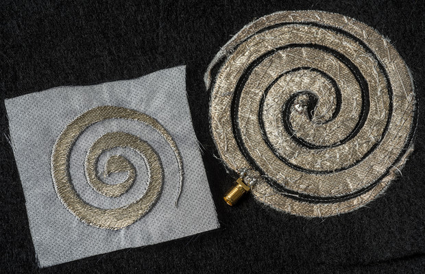
One prototype antenna looks like a spiral and can be embroidered into clothing to improve cell phone signal reception. Another prototype, a stretchable antenna with an integrated RFID (radio-frequency identification) chip embedded in rubber, takes the applications for the technology beyond clothing. (The latter object was part of a study done for a tire manufacturer.)

Yet another circuit resembles the Ohio State Block “O” logo, with non-conductive scarlet and gray thread embroidered among the silver wires “to demonstrate that e-textiles can be both decorative and functional,” Kiourti said.

They may be decorative, but the embroidered antennas and circuits actually work. Tests showed that an embroidered spiral antenna measuring approximately six inches across transmitted signals at frequencies of 1 to 5 GHz with near-perfect efficiency. The performance suggests that the spiral would be well-suited to broadband internet and cellular communication.

In other words, the shirt on your back could help boost the reception of the smart phone or tablet that you’re holding – or send signals to your devices with health or athletic performance data.

The work fits well with Ohio State’s role as a founding partner of the Advanced Functional Fabrics of America Institute, a national manufacturing resource center for industry and government. The new institute, which joins some 50 universities and industrial partners, was announced earlier this month by U.S. Secretary of Defense Ashton Carter.

Syscom Advanced Materials in Columbus provided the threads used in Volakis and Kiourti’s initial work. The finer threads used in this study were purchased from Swiss manufacturer Elektrisola. The research is funded by the National Science Foundation, and Ohio State will license the technology for further development.

Until then, Volakis is making out a shopping list for the next phase of the project.

“We want a bigger sewing machine,” he said.

Here’s a link to and a citation for the paper,

Fabrication of Textile Antennas and Circuits With 0.1 mm Precision by A. Kiourti, C. Lee, and J. L. Volakis.  IEEE Antennas and Wireless Propagation Letters (Volume:15 ) Page(s): 151 – 153 ISSN : 1536-1225 INSPEC Accession Number: 15785288 DOI: 10.1109/LAWP.2015.2435257 Date of Publication: 20 May 2015 Issue Date: 2016

This paper is behind a paywall.

$1.4B for US National Nanotechnology Initiative (NNI) in 2017 budget

According to an April 1, 2016 news item on Nanowerk, the US National Nanotechnology (NNI) has released its 2017 budget supplement,

The President’s Budget for Fiscal Year 2017 provides $1.4 billion for the National Nanotechnology Initiative (NNI), affirming the important role that nanotechnology continues to play in the Administration’s innovation agenda. NNI
Cumulatively totaling nearly $24 billion since the inception of the NNI in 2001, the President’s 2017 Budget supports nanoscale science, engineering, and technology R&D at 11 agencies.

Another 9 agencies have nanotechnology-related mission interests or regulatory responsibilities.

An April 1, 2016 NNI news release, which originated the news item, affirms the Obama administration’s commitment to the NNI and notes the supplement serves as an annual report amongst other functions,

Throughout its two terms, the Obama Administration has maintained strong fiscal support for the NNI and has implemented new programs and activities to engage the broader nanotechnology community to support the NNI’s vision that the ability to understand and control matter at the nanoscale will lead to new innovations that will improve our quality of life and benefit society.

This Budget Supplement documents progress of these participating agencies in addressing the goals and objectives of the NNI. It also serves as the Annual Report for the NNI called for under the provisions of the 21st Century Nanotechnology Research and Development Act of 2003 (Public Law 108-153, 15 USC §7501). The report also addresses the requirement for Department of Defense reporting on its nanotechnology investments, per 10 USC §2358.

For additional details and to view the full document, visit www.nano.gov/2017BudgetSupplement.

I don’t seem to have posted about the 2016 NNI budget allotment but 2017’s $1.4B represents a drop of $100M since 2015’s $1.5 allotment.

The 2017 NNI budget supplement describes the NNI’s main focus,

Over the past year, the NNI participating agencies, the White House Office of Science and Technology Policy (OSTP), and the National Nanotechnology Coordination Office (NNCO) have been charting the future directions of the NNI, including putting greater focus on promoting commercialization and increasing education and outreach efforts to the broader nanotechnology community. As part of this effort, and in keeping with recommendations from the 2014 review of the NNI by the President’s Council of Advisors for Science and Technology, the NNI has been working to establish Nanotechnology-Inspired Grand Challenges, ambitious but achievable goals that will harness nanotechnology to solve National or global problems and that have the potential to capture the public’s imagination. Based upon inputs from NNI agencies and the broader community, the first Nanotechnology-Inspired Grand Challenge (for future computing) was announced by OSTP on October 20, 2015, calling for a collaborative effort to “create a new type of computer that can proactively interpret and learn from data, solve unfamiliar problems using what it has learned, and operate with the energy efficiency of the human brain.” This Grand Challenge has generated broad interest within the nanotechnology community—not only NNI agencies, but also industry, technical societies, and private foundations—and planning is underway to address how the agencies and the community will work together to achieve this goal. Topics for additional Nanotechnology-Inspired Grand Challenges are under review.

Interestingly, it also offers an explanation of the images on its cover (Note: Links have been removed),

US_NNI_2017_budget_cover

About the cover

Each year’s National Nanotechnology Initiative Supplement to the President’s Budget features cover images illustrating recent developments in nanotechnology stemming from NNI activities that have the potential to make major contributions to National priorities. The text below explains the significance of each of the featured images on this year’s cover.

US_NNI_2017_front_cover_CloseUp

Front cover featured images (above): Images illustrating three novel nanomedicine applications. Center: microneedle array for glucose-responsive insulin delivery imaged using fluorescence microscopy. This “smart insulin patch” is based on painless microneedles loaded with hypoxia-sensitive vesicles ~100 nm in diameter that release insulin in response to high glucose levels. Dr. Zhen Gu and colleagues at the University of North Carolina (UNC) at Chapel Hill and North Carolina State University have demonstrated that this patch effectively regulates the blood glucose of type 1 diabetic mice with faster response than current pH-sensitive formulations. The inset image on the lower right shows the structure of the nanovesicles; each microneedle contains more than 100 million of these vesicles. The research was supported by the American Diabetes Association, the State of North Carolina, the National Institutes of Health (NIH), and the National Science Foundation (NSF). Left: colorized rendering of a candidate universal flu vaccine nanoparticle. The vaccine molecule, developed at the NIH Vaccine Research Center, displays only the conserved part of the viral spike and stimulates the production of antibodies to fight against the ever-changing flu virus. The vaccine is engineered from a ~13 nm ferritin core (blue) combined with a 7 nm influenza antigen (green). Image credit: NIH National Institute of Allergy and Infectious Diseases (NIAID). Right: colorized scanning electron micrograph of Ebola virus particles on an infected VERO E6 cell. Blue represents individual Ebola virus particles. The image was produced by John Bernbaum and Jiro Wada at NIAID. When the Ebola outbreak struck in 2014, the Food and Drug Administration authorized emergency use of lateral flow immunoassays for Ebola detection that use gold nanoparticles for visual interpretation of the tests.

US_NNI_2017_back_cover._CloseUp

Back cover featured images (above): Images illustrating examples of NNI educational outreach activities. Center: Comic from the NSF/NNI competition Generation Nano: Small Science Superheroes. Illustration by Amina Khan, NSF. Left of Center: Polymer Nanocone Array (biomimetic of antimicrobial insect surface) by Kyle Nowlin, UNC-Greensboro, winner from the first cycle of the NNI’s student image contest, EnvisioNano. Right of Center: Gelatin Nanoparticles in Brain (nasal delivery of stroke medication to the brain) by Elizabeth Sawicki, University of Illinois at Urbana-Champaign, winner from the second cycle of EnvisioNano. Outside right: still photo from the video Chlorination-less (water treatment method using reusable nanodiamond powder) by Abelardo Colon and Jennifer Gill, University of Puerto Rico at Rio Piedras, the winning video from the NNI’s Student Video Contest. Outside left: Society of Emerging NanoTechnologies (SENT) student group at the University of Central Florida, one of the initial nodes in the developing U.S. Nano and Emerging Technologies Student Network; photo by Alexis Vilaboy.

Vote for* winner for Generation Nano: Small Science, Superheroes

The US National Science Foundation’s (NSF) contest “Generation Nano: Small Science, Superheroes” for high school students has whittled down the entries to three finalists and bringing them to Washington, DC where the winner will announced at the 2016 USA Science & Engineering Festival (April 16 – 17, 2016) according to a March 30, 2016 NSF news release,

The National Science Foundation (NSF) today announced the names of three finalists in its Generation Nano: Small Science, Superheroes competition, sponsored by NSF and its National Nanotechnology Initiative (NNI) and supported by many, including superhero legend Stan Lee.

High school students Madeleine Chang from Bergen County Academies in New Jersey, Vuong Mai from Martha Ellen Stilwell School of the Arts in Georgia and Eric Liu from Thomas Jefferson High School for Science and Technology in Virginia will come to Washington, D.C., to display their comics and compete for prizes at the 2016 USA Science & Engineering Festival in mid-April.

The competition drew submissions from all over the country. All responded to the call to think big — or in this case small — and use nanotechnology to empower their own original superheroes. Chang’s hero “Radio Blitz” disposes of local waste. Mai’s protector “Nine” dons a Nanosuit for strength to save a kidnapping victim. And Liu’s “Nanoman” fights the malignant crab-monster, “Cancer.”

“These three finalists tell a great story — all while they exemplify the combination of a sound technical basis for use of nanotechnology and artistic presentation,” said Lisa Friedersdorf, deputy director of the National Nanotechnology Coordination Office. “I think these comics will inspire other students to learn more about what is possible with nanotechnology.”

When it comes to applications for nanotechnology, “The possibilities abound,” said Mihail C. Roco, NSF senior advisor for science and engineering and key architect of NNI.

“Since these high school students were born, more discoveries have come from nanotechnology than any other field of science, with its discoveries penetrating all aspects of society — new industries, medicine, agriculture and the management of natural resources,” Roco said. “It is so exciting that these kids are getting in on the ground floor of progress. The competition inspires young people to dream high and create solutions in a way that may change their lives and those around them. We need this new talent; the future of emerging technologies, including nanotechnology depends on it.”

Those of us who cannot attend the festival, can vote online,

And remember to vote for your favorite from April 7 to 15.

*ETA March 31, 2016 at 1115 hours PDT: The vote link from the news release does not seem to be operational presumably since we the voting period doesn’t start until April 7, 2016.

Congratulations to the three finalists!

*’or’ switched to ‘for’  in the headline at 1110 hours PDT on March 31, 2016.

Sensing fuel leaks and fuel-based explosives with a nanofibril composite

A March 28, 2016 news item on Nanowerk highlights some research from the University of Utah (US),

Alkane fuel is a key ingredient in combustible material such as gasoline, airplane fuel, oil — even a homemade bomb. Yet it’s difficult to detect and there are no portable scanners available that can sniff out the odorless and colorless vapor.

But University of Utah engineers have developed a new type of fiber material for a handheld scanner that can detect small traces of alkane fuel vapor, a valuable advancement that could be an early-warning signal for leaks in an oil pipeline, an airliner, or for locating a terrorist’s explosive.

A March 25, 2016 University of Utah news release, which originated the news item, provides a little more detail,

Currently, there are no small, portable chemical sensors to detect alkane fuel vapor because it is not chemically reactive. The conventional way to detect it is with a large oven-sized instrument in a lab.

“It’s not mobile and very heavy,” Zang [Ling Zang, University of Utah materials science and engineering professor] says of the larger instrument. “There’s no way it can be used in the field. Imagine trying to detect the leak from a gas valve or on the pipelines. You ought to have something portable.”

So Zang’s team developed a type of fiber composite that involves two nanofibers transferring electrons from one to the other.

That kind of interaction would then signal the detector that the alkane vapor is present. Vaporsens, a University of Utah spinoff company, has designed a prototype of the handheld detector with an array of 16 sensor materials that will be able to identify a broad range of chemicals including explosives.  This new composite material will be incorporated into the sensor array to include the detection of alkanes. Vaporsens plans to introduce the device on the market in about a year and a half, says Zang, who is the company’s chief science officer.

Such a small sensor device that can detect alkane vapor will benefit three main categories:

  • Oil pipelines. If leaks from pipelines are not detected early enough, the resulting leaked oil could contaminate the local environment and water sources. Typically, only large leaks in pipelines can be detected if there is a drop in pressure. Zang’s portable sensor — when placed along the pipeline — could detect much smaller leaks before they become bigger.
  • Airplane fuel tanks. Fuel for aircraft is stored in removable “bladders” made of flexible fabric. The only way a leak can be detected is by seeing the dyed fuel seeping from the plane and then removing the bladder to inspect it. Zang’s sensors could be placed around the bladder to warn a pilot if a leak is occurring in real time and where it is located.
  • Security. The scanner will be designed to locate the presence of explosives such as bombs at airports or in other buildings. Many explosives, such as the bomb used in the Oklahoma City bombing in 1995, use fuel oils like diesel as one of its major components. These fuel oils are forms of alkane.

The research was funded by the Department of Homeland Security, National Science Foundation and NASA. The lead author of the paper is University of Utah materials science and engineering doctoral student Chen Wang, and [Benjamin] Bunes is the co-author.

Here’s a link to and a citation for the paper,

Interfacial Donor–Acceptor Nanofibril Composites for Selective Alkane Vapor Detection by Chen Wang, Benjamin R. Bunes, Miao Xu, Na Wu, Xiaomei Yang, Dustin E. Gross, and Ling Zang. ACS Sens DOI: 10.1021/acssensors.6b00018 Publication Date (Web): March 09, 2016

Copyright © 2016 American Chemical Society

This paper is behind a paywall.

US Nanotechnology Initiative for water sustainability

Wednesday, March 23, 2016 was World Water Day and to coincide with that event the US National Nanotechnology Initiative (NNI) in collaboration with several other agencies announced a new ‘signature initiative’. From a March 24, 2016 news item on Nanowerk (Note: A link has been removed),

As a part of the White House Water Summit held yesterday on World Water Day, the Federal agencies participating in the National Nanotechnology Initiative (NNI) announced the launch of a Nanotechnology Signature Initiative (NSI), Water Sustainability through Nanotechnology: Nanoscale Solutions for a Global-Scale Challenge.

A March 23, 2016 NNI news release provides more information about why this initiative is important,

Access to clean water remains one of the world’s most pressing needs. As today’s White House Office of Science and Technology blog post explains, “the small size and exceptional properties of engineered nanomaterials are particularly promising for addressing the key technical challenges related to water quality and quantity.”

“One cannot find an issue more critical to human life and global security than clean, plentiful, and reliable water sources,” said Dr. Michael Meador, Director of the National Nanotechnology Coordination Office (NNCO). “Through the NSI mechanism, NNI member agencies will have an even greater ability to make meaningful strides toward this initiative’s thrust areas: increasing water availability, improving the efficiency of water delivery and use, and enabling next-generation water monitoring systems.”

A March 23, 2016 US White House blog posting by Lloyd Whitman and Lisa Friedersdorf describes the efforts in more detail (Note: A link has been removed),

The small size and exceptional properties of engineered nanomaterials are particularly promising for addressing the pressing technical challenges related to water quality and quantity. For example, the increased surface area—a cubic centimeter of nanoparticles has a surface area larger than a football field—and reactivity of nanometer-scale particles can be exploited to create catalysts for water purification that do not require rare or precious metals. And composites incorporating nanomaterials such as carbon nanotubes might one day enable stronger, lighter, and more durable piping systems and components. Under this NSI, Federal agencies will coordinate and collaborate to more rapidly develop nanotechnology-enabled solutions in three main thrusts: [thrust 1] increasing water availability; [thrust 2] improving the efficiency of water delivery and use; and [thrust 3] enabling next-generation water monitoring systems.

A technical “white paper” released by the agencies this week highlights key technical challenges for each thrust, identifies key objectives to overcome those challenges, and notes areas of research and development where nanotechnology promises to provide the needed solutions. By shining a spotlight on these areas, the new NSI will increase Federal coordination and collaboration, including with public and private stakeholders, which is vital to making progress in these areas. The additional focus and associated collective efforts will advance stewardship of water resources to support the essential food, energy, security, and environment needs of all stakeholders.

We applaud the commitment of the Federal agencies who will participate in this effort—the Department of Commerce/National Institute of Standards and Technology, Department of Energy, Environmental Protection Agency, National Aeronautics and Space Administration, National Science Foundation, and U.S. Department of Agriculture/National Institute of Food and Agriculture. As made clear at this week’s White House Water Summit, the world’s water systems are under tremendous stress, and new and emerging technologies will play a critical role in ensuring a sustainable water future.

The white paper (12 pp.) is titled: Water Sustainability through Nanotechnology: Nanoscale Solutions for a Global-Scale Challenge and describes the thrusts in more detail.

A March 22, 2016 US White House fact sheet lays out more details including funding,

Click here to learn more about all of the commitments and announcements being made today. They include:

  • Nearly $4 billion in private capital committed to investment in a broad range of water-infrastructure projects nationwide. This includes $1.5 billion from Ultra Capital to finance decentralized and scalable water-management solutions, and $500 million from Sustainable Water to develop water reclamation and reuse systems.
  • More than $1 billion from the private sector over the next decade to conduct research and development into new technologies. This includes $500 million from GE to fuel innovation, expertise, and global capabilities in advanced water, wastewater, and reuse technologies.
  • A Presidential Memorandum and supporting Action Plan on building national capabilities for long-term drought resilience in the United States, including by setting drought resilience policy goals, directing specific drought resilience activities to be completed by the end of the year, and permanently establishing the National Drought Resilience Partnership as an interagency task force responsible for coordinating drought-resilience, response, and recovery efforts.
  • Nearly $35 million this year in Federal grants from the Environmental Protection Agency, the National Oceanic and Atmospheric Administration, the National Science Foundation, and the U.S. Department of Agriculture to support cutting-edge water science;
  • The release of a new National Water Model that will dramatically enhance the Nation’s river-forecasting capabilities by delivering forecasts for approximately 2.7 million locations, up from 4,000 locations today (a 700-fold increase in forecast density).

This seems promising and hopefully other countries will follow suit.

A study in contrasts: innovation and education strategies in US and British Columbia (Canada)

It’s always interesting to contrast two approaches to the same issue, in this case, innovation and education strategies designed to improve the economies of the United States and of British Columbia, a province in Canada.

One of the major differences regarding education in the US and in Canada is that the Canadian federal government, unlike the US federal government, has no jurisdiction over the matter. Education is strictly a provincial responsibility.

I recently wrote a commentary (a Jan. 19, 2016 posting) about the BC government’s Jan. 18, 2016 announcement of its innovation strategy in a special emphasis on the education aspect. Premier Christy Clark focused largely on the notion of embedding courses on computer coding in schools from K-12 (kindergarten through grade 12) as Jonathon Narvey noted in his Jan. 19, 2016 event recap for Betakit,

While many in the tech sector will be focused on the short-term benefits of a quick injection of large capital [a $100M BC Tech Fund as part of a new strategy was announced in Dec. 2015 but details about the new #BCTECH Strategy were not shared until Jan. 18, 2016], the long-term benefits for the local tech sector are being seeded in local schools. More than 600,000 BC students will be getting basic skills in the K-12 curriculum, with coding academies, more work experience electives and partnerships between high school and post-secondary institutions.

Here’s what I had to say in my commentary (from the Jan. 19, 2016 posting),

… the government wants to embed  computer coding into the education system for K-12 (kindergarten to grade 12). One determined reporter (Canadian Press if memory serves) attempted to find out how much this would cost. No answer was forthcoming although there were many words expended. Whether this failure was due to ignorance (disturbing!) or a reluctance to share (also disturbing!) was impossible to tell. Another reporter (Georgia Straight) asked about equipment (coding can be taught with pen and paper but hardware is better). … Getting back to the reporter’s question, no answer was forthcoming although the speaker was loquacious.

Another reporter asked if the government had found any jurisdictions doing anything similar regarding computer coding. It seems they did consider other jurisdictions although it was claimed that BC is the first to strike out in this direction. Oddly, no one mentioned Estonia, known in some circles as E-stonia, where the entire school system was online by the late 1990s in an initiative known as the ‘Tiger Leap Foundation’ which also supported computer coding classes in secondary school (there’s more in Tim Mansel’s May 16, 2013 article about Estonia’s then latest initiative to embed computer coding into grade school.) …

Aside from the BC government’s failure to provide details, I am uncomfortable with what I see as an overemphasis on computer coding that suggests a narrow focus on what constitutes a science and technology strategy for education. I find the US approach closer to what I favour although I may be biased since they are building their strategy around nanotechnology education.

The US approach had been announced in dribs and drabs until recently when a Jan. 26, 2016 news item on Nanotechnology Now indicated a broad-based plan for nanotechnology education (and computer coding),

Over the past 15 years, the Federal Government has invested over $22 billion in R&D under the auspices of the National Nanotechnology Initiative (NNI) to understand and control matter at the nanoscale and develop applications that benefit society. As these nanotechnology-enabled applications become a part of everyday life, it is important for students to have a basic understanding of material behavior at the nanoscale, and some states have even incorporated nanotechnology concepts into their K-12 science standards. Furthermore, application of the novel properties that exist at the nanoscale, from gecko-inspired climbing gloves and invisibility cloaks, to water-repellent coatings on clothes or cellphones, can spark students’ excitement about science, technology, engineering, and mathematics (STEM).

An earlier Jan. 25, 2016 White House blog posting by Lisa Friedersdorf and Lloyd Whitman introduced the notion that nanotechnology is viewed as foundational and a springboard for encouraging interest in STEM (science, technology, engineering, and mathematics) careers while outlining several formal and information education efforts,

The Administration’s updated Strategy for American Innovation, released in October 2015, identifies nanotechnology as one of the emerging “general-purpose technologies”—a technology that, like the steam engine, electricity, and the Internet, will have a pervasive impact on our economy and our society, with the ability to create entirely new industries, create jobs, and increase productivity. To reap these benefits, we must train our Nation’s students for these high-tech jobs of the future. Fortunately, the multidisciplinary nature of nanotechnology and the unique and fascinating phenomena that occur at the nanoscale mean that nanotechnology is a perfect topic to inspire students to pursue careers in science, technology, engineering, and mathematics (STEM).

The Nanotechnology: Super Small Science series [mentioned in my Jan. 21, 2016 posting] is just the latest example of the National Nanotechnology Initiative (NNI)’s efforts to educate and inspire our Nation’s students. Other examples include:

The announcement about computer coding and courses being integrated in the US education curricula K-12 was made in US President Barack Obama’s 2016 State of the Union speech and covered in a Jan. 30, 2016 article by Jessica Hullinger for Fast Company,

In his final State Of The Union address earlier this month, President Obama called for providing hands-on computer science classes for all students to make them “job ready on day one.” Today, he is unveiling how he plans to do that with his upcoming budget.

The President’s Computer Science for All Initiative seeks to provide $4 billion in funding for states and an additional $100 million directly to school districts in a push to provide access to computer science training in K-12 public schools. The money would go toward things like training teachers, providing instructional materials, and getting kids involved in computer science early in elementary and middle school.

There are more details in the Hullinger’s article and in a Jan. 30, 2016 White House blog posting by Megan Smith,

Computer Science for All is the President’s bold new initiative to empower all American students from kindergarten through high school to learn computer science and be equipped with the computational thinking skills they need to be creators in the digital economy, not just consumers, and to be active citizens in our technology-driven world. Our economy is rapidly shifting, and both educators and business leaders are increasingly recognizing that computer science (CS) is a “new basic” skill necessary for economic opportunity and social mobility.

CS for All builds on efforts already being led by parents, teachers, school districts, states, and private sector leaders from across the country.

Nothing says one approach has to be better than the other as there’s usually more than one way to accomplish a set of goals. As well, it’s unfair to expect a provincial government to emulate the federal government of a larger country with more money to spend. I just wish the BC government (a) had shared details such as the budget allotment for their initiative and (b) would hint at a more imaginative, long range view of STEM education.

Going back to Estonia one last time, in addition to the country’s recent introduction of computer coding classes in grade school, it has also embarked on a nanotechnology/nanoscience educational and entrepreneurial programme as noted in my Sept. 30, 2014 posting,

The University of Tartu (Estonia) announced in a Sept. 29, 2014 press release an educational and entrepreneurial programme about nanotechnology/nanoscience for teachers and students,

To bring nanoscience closer to pupils, educational researchers of the University of Tartu decided to implement the European Union LLP Comenius project “Quantum Spin-Off – connecting schools with high-tech research and entrepreneurship”. The objective of the project is to build a kind of a bridge: at one end, pupils can familiarise themselves with modern science, and at the other, experience its application opportunities at high-tech enterprises. “We also wish to inspire these young people to choose a specialisation related to science and technology in the future,” added Lukk [Maarika Lukk, Coordinator of the project].

The pupils can choose between seven topics of nanotechnology: the creation of artificial muscles, microbiological fuel elements, manipulation of nanoparticles, nanoparticles and ionic liquids as oil additives, materials used in regenerative medicine, deposition and 3D-characterisation of atomically designed structures and a topic covered in English, “Artificial robotic fish with EAP elements”.

Learning is based on study modules in the field of nanotechnology. In addition, each team of pupils will read a scientific publication, selected for them by an expert of that particular field. In that way, pupils will develop an understanding of the field and of scientific texts. On the basis of the scientific publication, the pupils prepare their own research project and a business plan suitable for applying the results of the project.

In each field, experts of the University of Tartu will help to understand the topics. Participants will visit a nanotechnology research laboratory and enterprises using nanotechnologies.

The project lasts for two years and it is also implemented in Belgium, Switzerland and Greece.

As they say, time will tell.

NISE Net, the acronym remains the same but the name changes

NISE Net, the US Nanoscale Informal Science Education Network is winding down the nano and refocussing on STEM (science, technology, engineering, and mathematics). In short, NISE Net will now stand for National Informal STEM Education Network. Here’s more from the Jan. 7, 2016 NISE Net announcement in the January 2016 issue of the Nano Bite,

COMMUNITY NEWS

NISE Network is Transitioning to the National Informal STEM Education Network

Thank you for all the great work you have done over the past decade. It has opened up totally new possibilities for the decade ahead.

We are excited to let you know that with the completion of NSF funding for the Nanoscale Informal Science Education Network, and the soon-to-be-announced NASA [US National Aeronautics and Space Administration]-funded Space and Earth Informal STEM Education project, the NISE Network is transitioning to a new, ongoing identity as the National Informal STEM Education Network! While we’ll still be known as the NISE Net, network partners will now engage audiences across the United States in a range of STEM topics. Several new projects are already underway and others are in discussion for the future.

Current NISE Net projects include:

  • The original Nanoscale Informal Science Education Network (NISE Net), focusing on nanoscale science, engineering, and technology (funded by NSF and led by the Museum of Science, Boston)
  • Building with Biology, focusing on synthetic biology (funded by NSF and led by the Museum of Science with AAAS [American Association for the Advancement of Science], BioBuilder, and SynBerc [emphases mine])
  • Sustainability in Science Museums (funded by Walton Sustainability Solutions Initiatives and led by Arizona State University)
  • Transmedia Museum, focusing on science and society issues raised by Mary Shelley’s Frankenstein (funded by NSF and led by Arizona State University)
  • Space and Earth Informal STEM Education (funded by NASA and led by the Science Museum of Minnesota)

The “new” NISE Net will be led by the Science Museum of Minnesota in collaboration with the Museum of Science and Arizona State University. Network leadership, infrastructure, and participating organizations will include existing Network partners, and others attracted to the new topics. We will be in touch through the newsletter, blog, and website in the coming months to share more about our plans for the Network and its projects.

In the mean time, work is continuing with partners within the Nanoscale Informal Science Education Network throughout 2016, with an award end date of February 28, 2017. Although there will not be a new NanoDays 2016 kit, we encourage our partners to continue to engage audiences in nano by hosting NanoDays events in 2016 (March 26 – April 3) and in the years ahead using their existing kit materials. The Network will continue to host and update nisenet.org and the online catalog that includes 627 products of which 366 are NISE Net products (public and professional), 261 are Linked products, and 55 are Evaluation and Research reports. The Evaluation and Research team is continuing to work on final Network reports, and the Museum and Community Partnerships project has awarded 100 Explore Science physical kits to partners to create new or expanded collaborations with local community organizations to reach new underserved audiences not currently engaged in nano. These collaborative projects are taking place spring-summer 2016.

Thank you again for making this possible through your great work.

Best regards,

Larry Bell, Museum of Science
Paul Martin, Science Museum of Minnesota and
Rae Ostman, Arizona State University

As noted in previous posts, I’m quite interested in the synthetic biology focus the network has established in the last several months starting in late Spring 2015 and the mention of two (new-to-me) organizations, BioBuilder and Synberc piqued my interest.

I found this on the About the foundation page of the BioBuilder website,

What’s the best way to solve today’s health problems? Or hunger challenges? Address climate change concerns? Or keep the environment cleaner? These are big questions. And everyone can be part of the solutions. Everyone. Middle school students, teens, high school teachers.

At BioBuilder, we teach problem solving.
We bring current science to the classroom.
We engage our students to become real scientists — the problem solvers who will change the world.
At BioBuilder, we empower educators to be agents of educational reform by reconnecting teachers all across the country with their love of teaching and their own love of learning.

Synthetic biology programs living cells to tackle today’s challenges. Biofuels, safer foods, anti-malarial drugs, less toxic cancer treatment, biodegradable adhesives — all fuel young students’ imaginations. At BioBuilder, we empower students to tackle these big questions. BioBuilder’s curricula and teacher training capitalize on students’ need to know, to explore and to be part of solving real world problems. Developed by an award winning team out of MIT [Massachusetts Institute of Technology], BioBuilder is taught in schools across the country and supported by thought leaders in the STEM community.

BioBuilder proves that learning by doing works. And inspires.

As for Synberc, it is the Synthetic Biology Engineering Research Center and they has this to say about themselves on their About us page (Note: Links have been removed),

Synberc is a multi-university research center established in 2006 with a grant from the National Science Foundation (NSF) to help lay the foundation for synthetic biology Our mission is threefold:

develop the foundational understanding and technologies to build biological components and assemble them into integrated systems to accomplish many particular tasks;
train a new cadre of engineers who will specialize in engineering biology; and
engage the public about the opportunities and challenges of engineering biology.

Just as electrical engineers have made it possible for us to assemble computers from standardized parts (hard drives, memory cards, motherboards, and so on), we envision a day when biological engineers will be able to systematically assemble biological components such as sensors, signals, pathways, and logic gates in order to build bio-based systems that solve real-world problems in health, energy, and the environment.

In our work, we apply engineering principles to biology to develop tools that improve how fast — and how well — we can go through the design-test-build cycle. These include smart fermentation organisms that can sense their environment and adjust accordingly, and multiplex automated genome engineering, or MAGE, designed for large-scale programming and evolution of cells. We also pursue the discovery of applications that can lead to significant public benefit, such as synthetic artemisinin [emphasis mine], an anti-malaria drug that costs less and is more effective than the current plant-derived treatment.

The reference to ‘synthetic artemisinin’ caught my eye as I wrote an April 12, 2013 posting featuring this “… anti-malaria drug …” and the claim that the synthetic “… costs less and is more effective than the current plant-derived treatment” wasn’t quite the conclusion journalist, Brendan Borrell arrived at. Perhaps there’s been new research? If so, please let me know.

Canada has a nanotechnology industry? and an overview of the US situation

It’s always interesting to get some insight into how someone else sees the nanotechnology effort in Canada.

First, there have been two basic approaches internationally. Some countries have chosen to fund nanotechnology/nanoscience research through a national initiative/project/council/etc. Notably the US, the UK, China, and Russia, amongst others, have followed this model. For example, the US National Nanotechnology Initiative (NNI)  (a type of hub for research, communication, and commercialization efforts) has been awarded a portion of the US budget every year since 2000. The money is then disbursed through the National Science Foundation.

Canada and its nanotechnology industry efforts

By contrast, Canada has no such line item in its national budget. There is a National Institute of Nanotechnology (NINT) but it is one of many institutes that help make up Canada’s National Research Council. I’m not sure if this is still true but when it was first founded, NINT was funded in part by the federal government and in part by the province of Alberta where it is located (specifically, in Edmonton at the University of Alberta). They claim the organization has grown since its early days although it looks like it’s been shrinking. Perhaps some organizational shuffles? In any event, support for the Canadian nanotechnology efforts are more provincial than federal. Alberta (NINT and other agencies) and Québec (NanoQuébec, a provincially funded nano effort) are the standouts, with Ontario (nano Ontario, a self-organized not-for-profit group) following closely. The scene in Canada has always seemed fragmented in comparison to the countries that have nanotechnology ‘hubs’.

Patrick Johnson in a Dec. 22, 2015 article for Geopolitical Monitor offers a view which provides an overview of nanotechnology in the US and Canada,  adds to the perspective offered here, and, at times, challenges it (Note: A link has been added),

The term ‘nanotechnology’ entered into the public vernacular quite suddenly around the turn of the century, right around the same time that, when announcing the US National Nanotechnology Initiative (NNI) in 2001 [2000; see the American Association for the Advancement of Science webpage on Historical Trends in Federal R&D, scroll down to the National Nanotechnology Initiative and click on the Jpg or Excel links], President Bill Clinton declared that it would one day build materials stronger than steel, detect cancer at its inception, and store the vast records of the Library of Congress in a device the size of a sugar cube. The world of science fiction took matters even further. In his 2002 book Prey, Michael Creighton [Michael Crichton; see Wikipedia entry] wrote of a cloud of self-replicating nanorobots [also known as, nanobots or self-assemblers] that terrorize the good people of Nevada when a science experiment goes terribly wrong.

Back then the hype was palpable. Federal money was funneled to promising nanotech projects as not to fall behind in the race to master this new frontier of science. And industry analysts began to shoot for the moon in their projections. The National Science Foundation famously predicted that the nanotechnology industry would be worth $1 trillion by the year 2015.

Well here we are in 2015 and the nanotechnology market was worth around $26 billion in [sic] last year, and there hasn’t even been one case of a murderous swarm of nanomachines terrorizing the American heartland. [emphasis mine]

Is this a failure of vision? No. If anything it’s only a failure of timing.

The nanotechnology industry is still well on its way to accomplishing the goals set out at the founding of the NNI, goals which at the time sounded utterly quixotic, and this fact is increasingly being reflected in year-on-year growth numbers. In other words, nanotechnology is still a game-changer in global innovation, it’s just taking a little longer than first expected.

The Canadian Connection

Although the Canadian government is not among the world’s top spenders on nanotechnology research, the industry still represents a bright spot in the future of the Canadian economy. The public-private engine [emphasis mine] at the center of Canada’s nanotech industry, the National Institute for Nanotechnology (NINT), was founded in 2001 with the stated goal of “increasing the competitiveness of Canadian companies; creating technology solutions to meet the needs of society; expanding training programs for researchers and entrepreneurs; and enhancing Canada’s stature in the world of nanotechnology.” This ambitious mandate that NINT set out for itself was to be accomplished over the course of two broad stages: first a ‘seeding’ phase of attracting promising personnel and coordinating basic research, and the then a ‘harvesting’ phase of putting the resulting nanotechnologies to the service of Canadian industry.

Recent developments in Canadian nanotechnology [emphasis mine] show that we have already entered that second stage where the concept of nanotechnology transitions from hopeful hypothetical to real-world economic driver

I’d dearly like to know which recent developments indicate Canada’s industry has entered a serious commercialization phase. (It’s one of the shortcomings of our effort that communication is not well supported.) As well, I’d like to know more about the  “… public-private engine at the center of Canada’s nanotech industry …” as Johnson seems to be referring to the NINT, which is jointly funded (I believe) by the federal government and the province of Alberta. There is no mention of private funding on their National Research Council webpage but it does include the University of Alberta as a major supporter.

I am intrigued and I hope there is more information to come.

US and its nanotechnology industry efforts

Dr. Ambika Bumb has written a Dec. 23, 2015 article for Tech Crunch which reflects on her experience as a researcher and entrepreneur in the context of the US NNI effort and includes a plea for future NNI funding [Note: One link added and one link removed],

Indeed, I am fortunate to be the CEO of a nanomedicine technology developer that extends the hands of doctors and scientists to the cellular and molecular level.

The first seeds of interest in bringing effective nano-tools into the hands of doctors and patients were planted in my mind when I did undergrad research at Georgia Tech.  That initial interest led to me pursuing a PhD at Oxford University to develop a tri-modal nanoparticle for imaging a variety of diseases ranging from cancers to autoimmune disorders.

My graduate research only served to increase my curiosity so I then did a pair of post-doctoral fellowships at the National Cancer Institute and the National Heart Lung and Blood Institute.  When it seemed that I was a shoe-in for a life-long academic career, our technology garnered much attention and I found myself in the Bay Area founding the now award-winning Bikanta [bikanta.com].

Through the National Nanotechnology Initiative (NNI) and Nanotechnology Research and Development Act of 2003, our federal government has invested $20 billion in nanoresearch in the past 13 years.  The return on that investment has resulted in 628 agency‐to‐agency collaborations, hundreds of thousands of publications, and more than $1 trillion in revenue generated from nano‐enabled products. [emphasis mine]

Given that medical innovations take a minimum of 10 years before they translate into a clinical product, already realizing a 50X return is an astounding achievement.  Slowing down would be counter-intuitive from an academic and business perspective.

Yet, that is what is happening.  Federal funding peaked half a decade ago in 2010.  [emphasis mine] NNI investments went from $1.58B in 2010 to $1.170B in 2015 (in constant dollars), a 26% drop.  The number of nano-related papers published in the US were roughly 25 thousand in 2013, while the EU and China produced 33 and 35 thousand, respectively.

History has shown repeatedly how the United States has lost an early competitive advantage in developing high‐value technologies to international competition when commercialization infrastructure was not adequately supported.

Examples include semiconductors, advanced batteries for vehicles, and cement‐based construction materials, all of which were originally developed in the United States, but are now manufactured elsewhere.

It is now time for a second era – NNI 2.0.  A return to higher and sustained investment, the purpose of NNI 2.0 should be not just foundational research but also necessary support for rapid commercialization of nanotechnology. The translation of bench science into commercial reality requires the partnership of academic, industrial, federal, and philanthropic players.

I’m not sure why there’s a difference between Johnson’s ” … worth around $26 billion in [sic] last year …] and Bumb’s “… return on that investment has resulted … more than $1 trillion in revenue generated from nano‐enabled products.” I do know there is some controversy as to what should or should not be included when estimating the value of the ‘nanotechnology enterprise’, for example, products that are only possible due to nanotechnology as opposed to products that already existed, such as golf clubs, but are enhanced by nanotechnology.

Bumb goes on to provide a specific example from her own experience to support the plea,

When I moved from the renowned NIH [US National Institutes of Health] on the east coast to the west coast to start Bikanta, one of the highest priority concerns was how we were going to develop nanodiamond technology without access to high-end characterization instrumentation to analyze the quality of our material.  Purchasing all that equipment was not financially viable or even wise for a startup.

We were extremely lucky because our proposal was accepted by the Molecular Foundry, one of five DOE [US Department of Energy]-funded nanoscience user facilities.  While the Foundry primarily facilitates basic nanoscience projects from academic and national laboratory users, Fortune 500 companies and startups like ours also take advantage of its capabilities to answer fundamental questions and conduct proof of concept studies (~10%).

Disregarding the dynamic intellectual community for a minute, there is probably more than $150M worth of instrumentation at the Foundry.  An early startup would never be able to dream of raising a first round that large.

One of the factors of Bikanta’s success is that the Molecular Foundry enabled us to make tremendous strides in R&D in just months instead of years.  More user facilities, incubator centers, and funding for commercializing nanotech are greatly needed.

Final comments

I have to thank Dr. Bumb for pointing out that 2010 was the peak for NNI funding (see the American Association for the Advancement of Science webpage on Historical Trends in Federal R&D, scroll down to the National Nanotechnology Initiative and click on the Jpg or Excel links). I erroneously believed (although I don’t appear to have written up my belief; if you find any such statement, please let me know so I can correct it) that the 2015 US budget was the first time the NNI experienced a drop in funding.

While I found Johnson’s article interesting I wasn’t able to determine the source for his numbers and some of his material had errors that can be identified immediately, e.g., Michael Creighton instead of Michael Crichton.

A view to controversies about nanoparticle drug delivery, sticky-flares, and a PNAS surprise

Despite all the excitement and claims for nanoparticles as vehicles for drug delivery to ‘sick’ cells there is at least one substantive problem, the drug-laden nanoparticles don’t actually enter the interior of the cell. They are held in a kind of cellular ‘waiting room’.

Leonid Schneider in a Nov. 20, 2015 posting on his For Better Science blog describes the process in more detail,

A large body of scientific nanotechnology literature is dedicated to the biomedical aspect of nanoparticle delivery into cells and tissues. The functionalization of the nanoparticle surface is designed to insure their specificity at targeting only a certain type of cells, such as cancers cells. Other technological approaches aim at the cargo design, in order to ensure the targeted release of various biologically active agents: small pharmacological substances, peptides or entire enzymes, or nucleotides such as regulatory small RNAs or even genes. There is however a main limitation to this approach: though cells do readily take up nanoparticles through specific membrane-bound receptor interaction (endocytosis) or randomly (pinocytosis), these nanoparticles hardly ever truly reach the inside of the cell, namely its nucleocytoplasmic space. Solid nanoparticles are namely continuously surrounded by the very same membrane barrier they first interacted with when entering the cell. These outer-cell membrane compartments mature into endosomal and then lysosomal vesicles, where their cargo is subjected to low pH and enzymatic digestion. The nanoparticles, though seemingly inside the cell, remain actually outside. …

What follows is a stellar piece featuring counterclaims about and including Schneider’s own journalistic research into scientific claims that the problem of gaining entry to a cell’s true interior has been addressed by technologies developed in two different labs.

Having featured one of the technologies here in a July 24, 2015 posting titled: Sticky-flares nanotechnology to track and observe RNA (ribonucleic acid) regulation and having been contacted a couple of times by one of the scientists, Raphaël Lévy from the University of Liverpool (UK), challenging the claims made (Lévy’s responses can be found in the comments section of the July 2015 posting), I thought a followup of sorts was in order.

Scientific debates (then and now)

Scientific debates and controversies are part and parcel of the scientific process and what most outsiders, such as myself, don’t realize is how fraught it is. For a good example from the past, there’s Leviathan and the Air-Pump: Hobbes, Boyle, and the Experimental Life (from its Wikipedia entry), Note: Links have been removed),

Leviathan and the Air-Pump: Hobbes, Boyle, and the Experimental Life (published 1985) is a book by Steven Shapin and Simon Schaffer. It examines the debate between Robert Boyle and Thomas Hobbes over Boyle’s air-pump experiments in the 1660s.

The style seems more genteel than what a contemporary Canadian or US audience is accustomed to but Hobbes and Boyle (and proponents of both sides) engaged in bruising communication.

There was a lot at stake then and now. It’s not just the power, prestige, and money, as powerfully motivating as they are, it’s the research itself. Scientists work for years to achieve breakthroughs or to add more to our common store of knowledge. It’s painstaking and if you work at something for a long time, you tend to be invested in it. Saying you’ve wasted ten years of your life looking at the problem the wrong way or have misunderstood your data is not easy.

As for the current debate, Schneider’s description gives no indication that there is rancour between any of the parties but it does provide a fascinating view of two scientists challenging one of the US’s nanomedicine rockstars, Chad Mirkin. The following excerpt follows the latest technical breakthroughs to the interior portion of the cell through three phases of the naming conventions (Nano-Flares, also known by its trade name, SmartFlares, which is a precursor technology to Sticky-Flares), Note: Links have been removed,

The next family of allegedly nucleocytoplasmic nanoparticles which Lévy turned his attention to, was that of the so called “spherical nucleic acids”, developed in the lab of Chad Mirkin, multiple professor and director of the International Institute for Nanotechnology at the Northwestern University, USA. These so called “Nano-Flares” are gold nanoparticles, functionalized with fluorophore-coupled oligonucleotides matching the messenger RNA (mRNA) of interest (Prigodich et al., ACS Nano 3:2147-2152, 2009; Seferos et al., J Am. Chem.Soc. 129:15477-15479, 2007). The mRNA detection method is such that the fluorescence is initially quenched by the gold nanoparticle proximity. Yet when the oligonucleotide is displaced by the specific binding of the mRNA molecules present inside the cell, the fluorescence becomes detectable and serves thus as quantitative read-out for the intracellular mRNA abundance. Exactly this is where concerns arise. To find and bind mRNA, spherical nucleic acids must leave the endosomal compartments. Is there any evidence that Nano-Flares ever achieve this and reach intact the nucleocytoplasmatic space, where their target mRNA is?

Lévy’s lab has focused its research on the commercially available analogue of the Nano-Flares, based on the patent to Mirkin and Northwestern University and sold by Merck Millipore under the trade name of SmartFlares. These were described by Mirkin as “a powerful and prolific tool in biology and medical diagnostics, with ∼ 1,600 unique forms commercially available today”. The work, led by Lévy’s postdoctoral scientist David Mason, now available in post-publication process at ScienceOpen and on Figshare, found no experimental evidence for SmartFlares to be ever found outside the endosomal membrane vesicles. On the contrary, the analysis by several complementary approaches, i.e., electron, fluorescence and photothermal microscopy, revealed that the probes are retained exclusively within the endosomal compartments.

In fact, even Merck Millipore was apparently well aware of this problem when the product was developed for the market. As I learned, Merck performed a number of assays to address the specificity issue. Multiple hundred-fold induction of mRNA by biological cell stimulation (confirmed by quantitative RT-PCR) led to no significant changes in the corresponding SmartFlare signal. Similarly, biological gene downregulation or experimental siRNA knock-down had no effect on the corresponding SmartFlare fluorescence. Cell lines confirmed as negative for a certain biomarker proved highly positive in a SmartFlare assay.  Live cell imaging showed the SmartFlare signal to be almost entirely mitochondrial, inconsistent with reported patterns of the respective mRNA distributions.  Elsewhere however, cyanine dye-labelled oligonucleotides were found to unspecifically localise to mitochondria   (Orio et al., J. RNAi Gene Silencing 9:479-485, 2013), which might account to the often observed punctate Smart Flare signal.

More recently, Mirkin lab has developed a novel version of spherical nucleic acids, named Sticky-Flares (Briley et al., PNAS 112:9591-9595, 2015), which has also been patented for commercial use. The claim is that “the Sticky-flare is capable of entering live cells without the need for transfection agents and recognizing target RNA transcripts in a sequence-specific manner”. To confirm this, Lévy used the same approach as for the striped nanoparticles [not excerpted here]: he approached Mirkin by email and in person, requesting the original microscopy data from this publication. As Mirkin appeared reluctant, Lévy invoked the rules for data sharing by the journal PNAS, the funder NSF as well as the Northwestern University. After finally receiving Mirkin’s thin-optical microscopy data by air mail, Lévy and Mason re-analyzed it and determined the absence of any evidence for endosomal escape, while all Sticky-Flare particles appeared to be localized exclusively inside vesicular membrane compartments, i.e., endosomes (Mason & Levy, bioRxiv 2015).

I encourage you to read Schneider’s Nov. 20, 2015 posting in its entirety as these excerpts can’t do justice to it.

The PNAS surprise

PNAS (Proceedings of the National Academy of Science) published one of Mirkin’s papers on ‘Sticky-flares’ and is where scientists, Raphaël Lévy and David Mason, submitted a letter outlining their concerns with the ‘Sticky-flares’ research. Here’s the response as reproduced in Lévy’s Nov. 16, 2015 posting on his Rapha-Z-Lab blog

Dear Dr. Levy,

I regret to inform you that the PNAS Editorial Board has declined to publish your Letter to the Editor. After careful consideration, the Board has decided that your letter does not contribute significantly to the discussion of this paper.

Thank you for submitting your comments to PNAS.

Sincerely yours,
Inder Verma
Editor-in-Chief

Judge for yourself, Lévy’s and Mason’s letter can be found here (pdf) and here.

Conclusions

My primary interest in this story is in the view it provides of the scientific process and the importance of and difficulty associated with the debates.

I can’t venture an opinion about the research or the counterarguments other than to say that Lévy’s and Mason’s thoughtful challenge bears more examination than PNAS is inclined to accord. If their conclusions or Chad Mirkin’s are wrong, let that be determined in an open process.

I’ll leave the very last comment to Schneider who is both writer and cartoonist, from his Nov. 20, 2015 posting,

LeonidSchneiderImagination