Tag Archives: Switzerland

A nano fabrication technique used to create next generation heart valve

I am going to have take the researchers’ word that these somehow lead to healthy heart valve tissue,

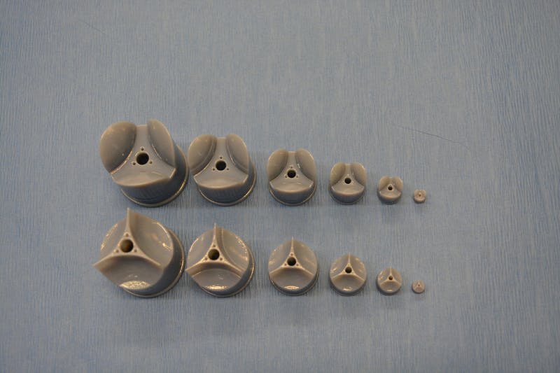
In rotary jet spinning technology, a rotating nozzle extrudes a solution of extracellular matrix (ECM) into nanofibers that wrap themselves around heart valve-shaped mandrels. By using a series of mandrels with different sizes, the manufacturing process becomes fully scalable and is able to provide JetValves for all age groups and heart sizes. Credit: Wyss Institute at Harvard University

From a May 18, 2017 news item on ScienceDaily,

The human heart beats approximately 35 million times every year, effectively pumping blood into the circulation via four different heart valves. Unfortunately, in over four million people each year, these delicate tissues malfunction due to birth defects, age-related deteriorations, and infections, causing cardiac valve disease.

Today, clinicians use either artificial prostheses or fixed animal and cadaver-sourced tissues to replace defective valves. While these prostheses can restore the function of the heart for a while, they are associated with adverse comorbidity and wear down and need to be replaced during invasive and expensive surgeries. Moreover, in children, implanted heart valve prostheses need to be replaced even more often as they cannot grow with the child.

A team lead by Kevin Kit Parker, Ph.D. at Harvard University’s Wyss Institute for Biologically Inspired Engineering recently developed a nanofiber fabrication technique to rapidly manufacture heart valves with regenerative and growth potential. In a paper published in Biomaterials, Andrew Capulli, Ph.D. and colleagues fabricated a valve-shaped nanofiber network that mimics the mechanical and chemical properties of the native valve extracellular matrix (ECM). To achieve this, the team used the Parker lab’s proprietary rotary jet spinning technology — in which a rotating nozzle extrudes an ECM solution into nanofibers that wrap themselves around heart valve-shaped mandrels. “Our setup is like a very fast cotton candy machine that can spin a range of synthetic and natural occurring materials. In this study, we used a combination of synthetic polymers and ECM proteins to fabricate biocompatible JetValves that are hemodynamically competent upon implantation and support cell migration and re-population in vitro. Importantly, we can make human-sized JetValves in minutes — much faster than possible for other regenerative prostheses,” said Parker.

A May 18,2017 Wyss Institute for Biologically Inspired Engineering news release (also on EurekAlert), which originated the news item, expands on the theme of Jetvalves,

To further develop and test the clinical potential of JetValves, Parker’s team collaborated with the translational team of Simon P. Hoerstrup, M.D., Ph.D., at the University of Zurich in Switzerland, which is a partner institution with the Wyss Institute. As a leader in regenerative heart prostheses, Hoerstrup and his team in Zurich have previously developed regenerative, tissue-engineered heart valves to replace mechanical and fixed-tissue heart valves. In Hoerstrup’s approach, human cells directly deposit a regenerative layer of complex ECM on biodegradable scaffolds shaped as heart valves and vessels. The living cells are then eliminated from the scaffolds resulting in an “off-the-shelf” human matrix-based prostheses ready for implantation.

In the paper, the cross-disciplinary team successfully implanted JetValves in sheep using a minimally invasive technique and demonstrated that the valves functioned properly in the circulation and regenerated new tissue. “In our previous studies, the cell-derived ECM-coated scaffolds could recruit cells from the receiving animal’s heart and support cell proliferation, matrix remodeling, tissue regeneration, and even animal growth. While these valves are safe and effective, their manufacturing remains complex and expensive as human cells must be cultured for a long time under heavily regulated conditions. The JetValve’s much faster manufacturing process can be a game-changer in this respect. If we can replicate these results in humans, this technology could have invaluable benefits in minimizing the number of pediatric re-operations,” said Hoerstrup.

In support of these translational efforts, the Wyss Institute for Biologically Inspired Engineering and the University of Zurich announced today a cross-institutional team effort to generate a functional heart valve replacement with the capacity for repair, regeneration, and growth. The team is also working towards a GMP-grade version of their customizable, scalable, and cost-effective manufacturing process that would enable deployment to a large patient population. In addition, the new heart valve would be compatible with minimally invasive procedures to serve both pediatric and adult patients.

The project will be led jointly by Parker and Hoerstrup. Parker is a Core Faculty member of the Wyss Institute and the Tarr Family Professor of Bioengineering and Applied Physics at the Harvard John A. Paulson School of Engineering and Applied Sciences (SEAS). Hoerstrup is Chair and Director of the University of Zurich’s Institute for Regenerative Medicine (IREM), Co-Director of the recently founded Wyss Translational Center Zurich and a Wyss Institute Associate Faculty member.

Since JetValves can be manufactured in all desired shapes and sizes, and take seconds to minutes to produce, the team’s goal is to provide customized, ready-to-use, regenerative heart valves much faster and at much lower cost than currently possible.

“Achieving the goal of minimally invasive, low-cost regenerating heart valves could have tremendous impact on patients’ lives across age-, social- and geographical boundaries. Once again, our collaborative team structure that combines unique and leading expertise in bioengineering, regenerative medicine, surgical innovation and business development across the Wyss Institute and our partner institutions, makes it possible for us to advance technology development in ways not possible in a conventional academic laboratory,” said Wyss Institute Founding Director Donald Ingber, M.D., Ph.D., who is also the Judah Folkman Professor of Vascular Biology at HMS and the Vascular Biology Program at Boston Children’s Hospital, as well as Professor of Bioengineering at SEAS.

This scanning electron microscopy image shows how extracellular matrix (ECM) nanofibers generated with JetValve technology are arranged in parallel networks with physical properties comparable to those found in native heart tissue. Credit: Wyss Institute at Harvard University

Here’s a link to and a citation for the paper,

JetValve: Rapid manufacturing of biohybrid scaffolds for biomimetic heart valve replacement by Andrew K. Capulli, Maximillian Y. Emmert, Francesco S. Pasqualini, b, Debora Kehl, Etem Caliskan, Johan U. Lind, Sean P. Sheehy, Sung Jin Park, Seungkuk Ahn, Benedikt Webe, Josue A. Goss. Biomaterials Volume 133, July 2017, Pages 229–241  https://doi.org/10.1016/j.biomaterials.2017.04.033

This paper is behind a paywall.

Nanoparticle behaviour in the environment unpredictable

These Swiss researchers took on a fairly massive project according to an April 19, 2017 news item on ScienceDaily,

The nanotech industry is booming. Every year, several thousands of tonnes of man-made nanoparticles are produced worldwide; sooner or later, a certain part of them will end up in bodies of water or soil. But even experts find it difficult to say exactly what happens to them there. It is a complex question, not only because there are many different types of man-made (engineered) nanoparticles, but also because the particles behave differently in the environment depending on the prevailing conditions.

Researchers led by Martin Scheringer, Senior Scientist at the Department of Chemistry and Applied Biosciences, wanted to bring some clarity to this issue. They reviewed 270 scientific studies, and the nearly 1,000 laboratory experiments described in them, looking for patterns in the behaviour of engineered nanoparticles. The goal was to make universal predictions about the behaviour of the particles.

An April 19, 2017ETH Zurich press release by Fabio Bergamin (also on EurekAlert), which originated the news item, elaborates,

Particles attach themselves to everything

However, the researchers found a very mixed picture when they looked at the data. “The situation is more complex than many scientists would previously have predicted,” says Scheringer. “We need to recognise that we can’t draw a uniform picture with the data available to us today.”

Nicole Sani-Kast, a doctoral student in Scheringer’s group and first author of the analysis published in the journal PNAS [Proceedings of the National Academy of Sciences], adds: “Engineered nanoparticles behave very dynamically and are highly reactive. They attach themselves to everything they find: to other nanoparticles in order to form agglomerates, or to other molecules present in the environment.”

Network analysis

To what exactly the particles react, and how quickly, depends on various factors such as the acidity of the water or soil, the concentration of the existing minerals and salts, and above all, the composition of the organic substances dissolved in the water or present in the soil. The fact that the engineered nanoparticles often have a surface coating makes things even more complicated. Depending on the environmental conditions, the particles retain or lose their coating, which in turn influences their reaction behaviour.

To evaluate the results available in the literature, Sani-Kast used a network analysis for the first time in this research field. It is a technique familiar in social research for measuring networks of social relations, and allowed her to show that the data available on engineered nanoparticles is inconsistent, insufficiently diverse and poorly structured.

More method for machine learning

“If more structured, consistent and sufficiently diverse data were available, it may be possible to discover universal patterns using machine learning methods,” says Scheringer, “but we’re not there yet.” Enough structured experimental data must first be available.

“In order for the scientific community to carry out such experiments in a systematic and standardised manner, some kind of coordination is necessary,” adds Sani-Kast, but she is aware that such work is difficult to coordinate. Scientists are generally well known for preferring to explore new methods and conditions rather than routinely performing standardized experiments.

[additional material]

Distinguishing man-made and natural nanoparticles

In addition to the lack of systematic research, there is also a second tangible problem in researching the behaviour of engineered nanoparticles: many engineered nanoparticles consist of chemical compounds that occur naturally in the soil. So far it has been difficult to measure the engineered particles in the environment since it is hard to distinguish them from naturally occurring particles with the same chemical composition.

However, researchers at ETH Zurich’s Department of Chemistry and Applied Biosciences, under the direction of ETH Professor Detlef Günther, have recently established an effective method that makes such a distinction possible in routine investigations. They used a state-of-the-art and highly sensitive mass spectrometry technique (called spICP-TOF mass spectrometry) to determine which chemical elements make up individual nanoparticles in a sample.

In collaboration with scientists from the University of Vienna, the ETH researchers applied the method to soil samples with natural cerium-containing particles, into which they mixed engineered cerium dioxide nanoparticles. Using machine learning methods, which were ideally suited to this particular issue, the researchers were able to identify differences in the chemical fingerprints of the two particle classes. “While artificially produced nanoparticles often consist of a single compound, natural nanoparticles usually still contain a number of additional chemical elements,” explains Alexander Gundlach-Graham, a postdoc in Günther’s group.

The new measuring method is very sensitive: the scientists were able to measure engineered particles in samples with up to one hundred times more natural particles.

The researchers have produced a visualization of their network analysis,

The researchers evaluated the experimental data published in the scientific literature using a network analysis. This analysis reveals which types of nanoparticles (blue) have been studied under which environmental conditions (red). (Visualisations: Thomas Kast)

Here are links and citation for two papers associated with this research,

A network perspective reveals decreasing material diversity in studies on nanoparticle interactions with dissolved organic matter by Nicole Sani-Kast, Jérôme Labille, Patrick Ollivier, Danielle Slomberg, Konrad Hungerbühler, and Martin Scheringer. PNAS 2017, 114: E1756-E1765, DOI: 10.1073/pnas.1608106114

Single-particle multi-element fingerprinting (spMEF) using inductively-coupled plasma time-of-flight mass spectrometry (ICP-TOFMS) to identify engineered nanoparticles against the elevated natural background in soils by Antonia Praetorius, Alexander Gundlach-Graham, Eli Goldberg, Willi Fabienke, Jana Navratilova, Andreas Gondikas, Ralf Kaegi, Detlef Günther, Thilo Hofmann, and Frank von der Kammer. Environonmental Science: Nano 2017, 4: 307-314, DOI: 10.1039/c6en00455e

Both papers are behind a paywall.

Nanocar Race winners!

In fact, there was a tie although it seems the Swiss winners were a little more excited. A May 1, 2017 news item on swissinfo.ch provides fascinating detail,

“Swiss Nano Dragster”, driven by scientists from Basel, has won the first international car race involving molecular machines. The race involved four nano cars zipping round a pure gold racetrack measuring 100 nanometres – or one ten-thousandth of a millimetre.

The two Swiss pilots, Rémy Pawlak and Tobias Meier from the Swiss Nanoscience Institute and the Department of Physicsexternal link at the University of Basel, had to reach the chequered flag – negotiating two curves en route – within 38 hours. [emphasis mine*]

The winning drivers, who actually shared first place with a US-Austrian team, were not sitting behind a steering wheel but in front of a computer. They used this to propel their single-molecule vehicle with a small electric shock from a scanning tunnelling microscope.

During such a race, a tunnelling current flows between the tip of the microscope and the molecule, with the size of the current depending on the distance between molecule and tip. If the current is high enough, the molecule starts to move and can be steered over the racetrack, a bit like a hovercraft.

….

The race track was maintained at a very low temperature (-268 degrees Celsius) so that the molecules didn’t move without the current.

What’s more, any nudging of the molecule by the microscope tip would have led to disqualification.

Miniature motors

The race, held in Toulouse, France, and organised by the National Centre for Scientific Research (CNRS), was originally going to be held in October 2016, but problems with some cars resulted in a slight delay. In the end, organisers selected four of nine applicants since there were only four racetracks.

The cars measured between one and three nanometres – about 30,000 times smaller than a human hair. The Swiss Nano Dragster is, in technical language, a 4′-(4-Tolyl)-2,2′:6′,2”-terpyridine molecule.

The Swiss and US-Austrian teams outraced rivals from the US and Germany.

The race is not just a bit of fun for scientists. The researchers hope to gain insights into how molecules move.

I believe this Basel University .gif is from the race,

*Emphasis added on May 9, 2017 at 12:26 pm PT. See my May 9, 2017 posting: Nanocar Race winners: The US-Austrian team for the other half of this story.

Bidirectional prosthetic-brain communication with light?

The possibility of not only being able to make a prosthetic that allows a tetraplegic to grab a coffee but to feel that coffee  cup with their ‘hand’ is one step closer to reality according to a Feb. 22, 2017 news item on ScienceDaily,

Since the early seventies, scientists have been developing brain-machine interfaces; the main application being the use of neural prosthesis in paralyzed patients or amputees. A prosthetic limb directly controlled by brain activity can partially recover the lost motor function. This is achieved by decoding neuronal activity recorded with electrodes and translating it into robotic movements. Such systems however have limited precision due to the absence of sensory feedback from the artificial limb. Neuroscientists at the University of Geneva (UNIGE), Switzerland, asked whether it was possible to transmit this missing sensation back to the brain by stimulating neural activity in the cortex. They discovered that not only was it possible to create an artificial sensation of neuroprosthetic movements, but that the underlying learning process occurs very rapidly. These findings, published in the scientific journal Neuron, were obtained by resorting to modern imaging and optical stimulation tools, offering an innovative alternative to the classical electrode approach.

A Feb. 22, 2017 Université de Genève press release on EurekAlert, which originated the news item, provides more detail,

Motor function is at the heart of all behavior and allows us to interact with the world. Therefore, replacing a lost limb with a robotic prosthesis is the subject of much research, yet successful outcomes are rare. Why is that? Until this moment, brain-machine interfaces are operated by relying largely on visual perception: the robotic arm is controlled by looking at it. The direct flow of information between the brain and the machine remains thus unidirectional. However, movement perception is not only based on vision but mostly on proprioception, the sensation of where the limb is located in space. “We have therefore asked whether it was possible to establish a bidirectional communication in a brain-machine interface: to simultaneously read out neural activity, translate it into prosthetic movement and reinject sensory feedback of this movement back in the brain”, explains Daniel Huber, professor in the Department of Basic Neurosciences of the Faculty of Medicine at UNIGE.

Providing artificial sensations of prosthetic movements

In contrast to invasive approaches using electrodes, Daniel Huber’s team specializes in optical techniques for imaging and stimulating brain activity. Using a method called two-photon microscopy, they routinely measure the activity of hundreds of neurons with single cell resolution. “We wanted to test whether mice could learn to control a neural prosthesis by relying uniquely on an artificial sensory feedback signal”, explains Mario Prsa, researcher at UNIGE and the first author of the study. “We imaged neural activity in the motor cortex. When the mouse activated a specific neuron, the one chosen for neuroprosthetic control, we simultaneously applied stimulation proportional to this activity to the sensory cortex using blue light”. Indeed, neurons of the sensory cortex were rendered photosensitive to this light, allowing them to be activated by a series of optical flashes and thus integrate the artificial sensory feedback signal. The mouse was rewarded upon every above-threshold activation, and 20 minutes later, once the association learned, the rodent was able to more frequently generate the correct neuronal activity.

This means that the artificial sensation was not only perceived, but that it was successfully integrated as a feedback of the prosthetic movement. In this manner, the brain-machine interface functions bidirectionally. The Geneva researchers think that the reason why this fabricated sensation is so rapidly assimilated is because it most likely taps into very basic brain functions. Feeling the position of our limbs occurs automatically, without much thought and probably reflects fundamental neural circuit mechanisms. This type of bidirectional interface might allow in the future more precisely displacing robotic arms, feeling touched objects or perceiving the necessary force to grasp them.

At present, the neuroscientists at UNIGE are examining how to produce a more efficient sensory feedback. They are currently capable of doing it for a single movement, but is it also possible to provide multiple feedback channels in parallel? This research sets the groundwork for developing a new generation of more precise, bidirectional neural prostheses.

Towards better understanding the neural mechanisms of neuroprosthetic control

By resorting to modern imaging tools, hundreds of neurons in the surrounding area could also be observed as the mouse learned the neuroprosthetic task. “We know that millions of neural connections exist. However, we discovered that the animal activated only the one neuron chosen for controlling the prosthetic action, and did not recruit any of the neighbouring neurons”, adds Daniel Huber. “This is a very interesting finding since it reveals that the brain can home in on and specifically control the activity of just one single neuron”. Researchers can potentially exploit this knowledge to not only develop more stable and precise decoding techniques, but also gain a better understanding of most basic neural circuit functions. It remains to be discovered what mechanisms are involved in routing signals to the uniquely activated neuron.

Caption: A novel optical brain-machine interface allows bidirectional communication with the brain. While a robotic arm is controlled by neuronal activity recorded with optical imaging (red laser), the position of the arm is fed back to the brain via optical microstimulation (blue laser). Credit: © Daniel Huber, UNIGE

Here’s a link to and a citation for the paper,

Rapid Integration of Artificial Sensory Feedback during Operant Conditioning of Motor Cortex Neurons by Mario Prsa, Gregorio L. Galiñanes, Daniel Huber. Neuron Volume 93, Issue 4, p929–939.e6, 22 February 2017 DOI: http://dx.doi.org/10.1016/j.neuron.2017.01.023 Open access funded by European Research Council

This paper is open access.

Imprinting fibres at the nanometric scale

Switzerland’s École Polytechnique Fédérale de Lausanne (EPFL) announces a discovery in a Jan. 24, 2017 press release (also on EurkeAlert),

Researchers at EPFL have come up with a way of imprinting nanometric patterns on the inside and outside of polymer fibers. These fibers could prove useful in guiding nerve regeneration and producing optical effects, for example, as well as in eventually creating artificial tissue and smart bandages.

Researchers at EPFL’s Laboratory of Photonic Materials and Fibre Devices, which is run by Fabien Sorin, have come up with a simple and innovative technique for drawing or imprinting complex, nanometric patterns on hollow polymer fibers. Their work has been published in Advanced Functional Materials.

The potential applications of this breakthrough are numerous. The imprinted designs could be used to impart certain optical effects on a fiber or make it water-resistant. They could also guide stem-cell growth in textured fiber channels or be used to break down the fiber at a specific location and point in time in order to release drugs as part of a smart bandage.

Stretching the fiber like molten plastic

To make their nanometric imprints, the researchers began with a technique called thermal drawing, which is the technique used to fabricate optical fibers. Thermal drawing involves engraving or imprinting millimeter-sized patterns on a preform, which is a macroscopic version of the target fiber. The imprinted preform is heated to change its viscosity, stretched like molten plastic into a long, thin fiber and then allowed to harden again. Stretching causes the pattern to shrink while maintaining its proportions and position. Yet this method has a major shortcoming: the pattern does not remain intact below the micrometer scale. “When the fiber is stretched, the surface tension of the structured polymer causes the pattern to deform and even disappear below a certain size, around several microns,” said Sorin.

To avoid this problem, the EPFL researchers came up with the idea of sandwiching the imprinted preform in a sacrificial polymer [emphasis mine]. This polymer protects the pattern during stretching by reducing the surface tension. It is discarded once the stretching is complete. Thanks to this trick, the researchers are able to apply tiny and highly complex patterns to various types of fibers. “We have achieved 300-nanometer patterns, but we could easily make them as small as several tens of nanometers,” said Sorin. This is the first time that such minute and highly complex patterns have been imprinted on flexible fiber on a very large scale. “This technique enables to achieve textures with feature sizes two order of magnitude smaller than previously reported,” said Sorin. “It could be applied to kilometers of fibers at a highly reasonable cost.”

To highlight potential applications of their achievement, the researchers teamed up with the Bertarelli Foundation Chair in Neuroprosthetic Technology, led by Stéphanie Lacour. Working in vitro, they were able to use their fibers to guide neurites from a spinal ganglion (on the spinal nerve). This was an encouraging step toward using these fibers to help nerves regenerate or to create artificial tissue.

This development could have implications in many other fields besides biology. “Fibers that are rendered water-resistant by the pattern could be used to make clothes. Or we could give the fibers special optical effects for design or detection purposes. There is also much to be done with the many new microfluidic systems out there,” said Sorin. The next step for the researchers will be to join forces with other EPFL labs on initiatives such as studying in vivo nerve regeneration. All this, thanks to the wonder of imprinted polymer fibers.

I like the term “sacrificial polymer.”

Here’s a link to and a citation for the paper,

Controlled Sub-Micrometer Hierarchical Textures Engineered in Polymeric Fibers and Microchannels via Thermal Drawing by Tung Nguyen-Dang, Alba C. de Luca, Wei Yan, Yunpeng Qu, Alexis G. Page, Marco Volpi, Tapajyoti Das Gupta, Stéphanie P. Lacour, and Fabien Sorin. Advanced Functional Materials DOI: 10.1002/adfm.201605935 Version of Record online: 24 JAN 2017

© 2017 WILEY-VCH Verlag GmbH & Co. KGaA, Weinheim

This paper is behind a paywall.

Developing cortical implants for future speech neural prostheses

I’m guessing that graphene will feature in these proposed cortical implants since the project leader is a member of the Graphene Flagship’s Biomedical Technologies Work Package. (For those who don’t know, the Graphene Flagship is one of two major funding initiatives each receiving funding of 1B Euros over 10 years from the European Commission as part of their FET [Future and Emerging Technologies)] Initiative.)  A Jan. 12, 2017 news item on Nanowerk announces the new project (Note: A link has been removed),

BrainCom is a FET Proactive project, funded by the European Commission with 8.35M€ [8.3 million Euros] for the next 5 years, holding its Kick-off meeting on January 12-13 at ICN2 (Catalan Institute of Nanoscience and Nanotechnology) and the UAB [ Universitat Autònoma de Barcelona]. This project, coordinated by ICREA [Catalan Institution for Research and Advanced Studies] Research Prof. Jose A. Garrido from ICN2, will permit significant advances in understanding of cortical speech networks and the development of speech rehabilitation solutions using innovative brain-computer interfaces.

A Jan. 12, 2017 ICN2 press release, which originated the news item expands on the theme (it is a bit repetitive),

More than 5 million people worldwide suffer annually from aphasia, an extremely invalidating condition in which patients lose the ability to comprehend and formulate language after brain damage or in the course of neurodegenerative disorders. Brain-computer interfaces (BCIs), enabled by forefront technologies and materials, are a promising approach to treat patients with aphasia. The principle of BCIs is to collect neural activity at its source and decode it by means of electrodes implanted directly in the brain. However, neurorehabilitation of higher cognitive functions such as language raises serious issues. The current challenge is to design neural implants that cover sufficiently large areas of the brain to allow for reliable decoding of detailed neuronal activity distributed in various brain regions that are key for language processing.

BrainCom is a FET Proactive project funded by the European Commission with 8.35M€ for the next 5 years. This interdisciplinary initiative involves 10 partners including technologists, engineers, biologists, clinicians, and ethics experts. They aim to develop a new generation of neuroprosthetic cortical devices enabling large-scale recordings and stimulation of cortical activity to study high level cognitive functions. Ultimately, the BraimCom project will seed a novel line of knowledge and technologies aimed at developing the future generation of speech neural prostheses. It will cover different levels of the value chain: from technology and engineering to basic and language neuroscience, and from preclinical research in animals to clinical studies in humans.

This recently funded project is coordinated by ICREA Prof. Jose A. Garrido, Group Leader of the Advanced Electronic Materials and Devices Group at the Institut Català de Nanociència i Nanotecnologia (Catalan Institute of Nanoscience and Nanotechnology – ICN2) and deputy leader of the Biomedical Technologies Work Package presented last year in Barcelona by the Graphene Flagship. The BrainCom Kick-Off meeting is held on January 12-13 at ICN2 and the Universitat Autònoma de Barcelona (UAB).

Recent developments show that it is possible to record cortical signals from a small region of the motor cortex and decode them to allow tetraplegic [also known as, quadriplegic] people to activate a robotic arm to perform everyday life actions. Brain-computer interfaces have also been successfully used to help tetraplegic patients unable to speak to communicate their thoughts by selecting letters on a computer screen using non-invasive electroencephalographic (EEG) recordings. The performance of such technologies can be dramatically increased using more detailed cortical neural information.

BrainCom project proposes a radically new electrocorticography technology taking advantage of unique mechanical and electrical properties of novel nanomaterials such as graphene, 2D materials and organic semiconductors.  The consortium members will fabricate ultra-flexible cortical and intracortical implants, which will be placed right on the surface of the brain, enabling high density recording and stimulation sites over a large area. This approach will allow the parallel stimulation and decoding of cortical activity with unprecedented spatial and temporal resolution.

These technologies will help to advance the basic understanding of cortical speech networks and to develop rehabilitation solutions to restore speech using innovative brain-computer paradigms. The technology innovations developed in the project will also find applications in the study of other high cognitive functions of the brain such as learning and memory, as well as other clinical applications such as epilepsy monitoring.

The BrainCom project Consortium members are:

  • Catalan Institute of Nanoscience and Nanotechnology (ICN2) – Spain (Coordinator)
  • Institute of Microelectronics of Barcelona (CNM-IMB-CSIC) – Spain
  • University Grenoble Alpes – France
  • ARMINES/ Ecole des Mines de St. Etienne – France
  • Centre Hospitalier Universitaire de Grenoble – France
  • Multichannel Systems – Germany
  • University of Geneva – Switzerland
  • University of Oxford – United Kingdom
  • Ludwig-Maximilians-Universität München – Germany
  • Wavestone – Luxembourg

There doesn’t seem to be a website for the project but there is a BrainCom webpage on the European Commission’s CORDIS (Community Research and Development Information Service) website.

Luminous electronic tiles (lumentile)

A Dec. 19, 2016 news item on Nanowerk introduces a ceramic tile that can be given a different look at the touch of a fingertip,

Using pioneering photonics technology, The ‘Luminous Electronic Tile’, or LUMENTILE, project mixes the simplicity of a plain ceramic tile with the complexity of today’s sophisticated touch screen technology, creating a light source and unparalleled interaction. All it takes is one tap to change the colour, look or mood of any room in your house.

This is the first time anyone has tried to embed electronics into ceramics or glass for a large-scale application. With the ability to play videos or display images, the tiles allow the user to turn their walls into a large ‘cinema’ screen, where each unit acts as a set of pixels of the overall display.

An undated Horizon 2020 webpage describes the ‘digital wallpaper’ in more detail,

Scientists from Italy have created ‘digital wallpaper’, allowing for a constant change in design and aesthetic controlled via a smartphone, tablet or computer.

Each Luminous Electronic Tile – or Lumentile – acts as a touch screen which can change colour, pattern or light intensity, play videos or display images.

If numerous tiles are arranged together, they can create a ‘cinema’ screen with each tile acting as a set of pixels for the overall display.

The combination of ceramic, glass and electronics could allow the user to have interchangeable control of the look and design of their surroundings by tapping the tile.

Each tile can be arranged to completely or partially cover walls of a room, floor or ceiling.

However, they can also be transferred to the exterior of buildings, as either flat or curved tiles to fit around columns or uneven surfaces.

Project co-ordinator Professor Guido Giuliani, said: “It may sound like the stuff of James Bond but external tiles would create a ‘chameleonic skin’ or instant camouflage.

“Although we are a long way off this yet, this would allow a car or building to blend completely into its surroundings, and hence ‘disappear’.”

Although these tiles cannot be purchased yet, they hope to be available to users in two years, with mass production by the end of 2020.

Lumentile received a grant of more than €2.4m from the Horizon 2020 programme via the Photonics Public Private Partnership. Created in Italy by the Universita Degli Studi Di Pavia, the Lumentile project also has a number of European partners from Finland, Switzerland and Spain.

A combination of ceramic, glass and organic electronics, the luminous tile includes structural materials, solid-state light sources and electronic chips and can be controlled with a central computer, a smart phone or tablet. [downloaded from http://www.nanowerk.com/nanotechnology-news/newsid=45417.php]

You can find a bit more information on the Lumentile project website.

Sustainable Nanotechnologies (SUN) project draws to a close in March 2017

Two Oct. 31, 2016 news item on Nanowerk signal the impending sunset date for the European Union’s Sustainable Nanotechnologies (SUN) project. The first Oct. 31, 2016 news item on Nanowerk describes the projects latest achievements,

The results from the 3rd SUN annual meeting showed great advancement of the project. The meeting was held in Edinburgh, Scotland, UK on 4-5 October 2016 where the project partners presented the results obtained during the second reporting period of the project.

SUN is a three and a half year EU project, running from 2013 to 2017, with a budget of about €14 million. Its main goal is to evaluate the risks along the supply chain of engineered nanomaterials and incorporate the results into tools and guidelines for sustainable manufacturing.

The ultimate goal of the SUN Project is the development of an online software Decision Support System – SUNDS – aimed at estimating and managing occupational, consumer, environmental and public health risks from nanomaterials in real industrial products along their lifecycles. The SUNDS beta prototype has been released last October, 2015, and since then the main focus has been on refining the methodologies and testing them on selected case studies i.e. nano-copper oxide based wood preserving paint and nano- sized colourants for plastic car part: organic pigment and carbon black. Obtained results and open issues were discussed during the third annual meeting in order collect feedbacks from the consortium that will inform, in the next months, the implementation of the final version of the SUNDS software system, due by March 2017.

An Oct. 27, 2016 SUN project press release, which originated the news item, adds more information,

Significant interest has been payed towards the results obtained in WP2 (Lifecycle Thinking) which main objectives are to assess the environmental impacts arising from each life cycle stage of the SUN case studies (i.e. Nano-WC-Cobalt (Tungsten Carbide-cobalt) sintered ceramics, Nanocopper wood preservatives, Carbon Nano Tube (CNT) in plastics, Silicon Dioxide (SiO2) as food additive, Nano-Titanium Dioxide (TiO2) air filter system, Organic pigment in plastics and Nanosilver (Ag) in textiles), and compare them to conventional products with similar uses and functionality, in order to develop and validate criteria and guiding principles for green nano-manufacturing. Specifically, the consortium partner COLOROBBIA CONSULTING S.r.l. expressed its willingness to exploit the results obtained from the life cycle assessment analysis related to nanoTiO2 in their industrial applications.

On 6th October [2016], the discussions about the SUNDS advancement continued during a Stakeholder Workshop, where representatives from industry, regulatory and insurance sectors shared their feedback on the use of the decision support system. The recommendations collected during the workshop will be used for the further refinement and implemented in the final version of the software which will be released by March 2017.

The second Oct. 31, 2016 news item on Nanowerk led me to this Oct. 27, 2016 SUN project press release about the activities in the upcoming final months,

The project has designed its final events to serve as an effective platform to communicate the main results achieved in its course within the Nanosafety community and bridge them to a wider audience addressing the emerging risks of Key Enabling Technologies (KETs).

The series of events include the New Tools and Approaches for Nanomaterial Safety Assessment: A joint conference organized by NANOSOLUTIONS, SUN, NanoMILE, GUIDEnano and eNanoMapper to be held on 7 – 9 February 2017 in Malaga, Spain, the SUN-CaLIBRAte Stakeholders workshop to be held on 28 February – 1 March 2017 in Venice, Italy and the SRA Policy Forum: Risk Governance for Key Enabling Technologies to be held on 1- 3 March in Venice, Italy.

Jointly organized by the Society for Risk Analysis (SRA) and the SUN Project, the SRA Policy Forum will address current efforts put towards refining the risk governance of emerging technologies through the integration of traditional risk analytic tools alongside considerations of social and economic concerns. The parallel sessions will be organized in 4 tracks:  Risk analysis of engineered nanomaterials along product lifecycle, Risks and benefits of emerging technologies used in medical applications, Challenges of governing SynBio and Biotech, and Methods and tools for risk governance.

The SRA Policy Forum has announced its speakers and preliminary Programme. Confirmed speakers include:

  • Keld Alstrup Jensen (National Research Centre for the Working Environment, Denmark)
  • Elke Anklam (European Commission, Belgium)
  • Adam Arkin (University of California, Berkeley, USA)
  • Phil Demokritou (Harvard University, USA)
  • Gerard Escher (École polytechnique fédérale de Lausanne, Switzerland)
  • Lisa Friedersdor (National Nanotechnology Initiative, USA)
  • James Lambert (President, Society for Risk Analysis, USA)
  • Andre Nel (The University of California, Los Angeles, USA)
  • Bernd Nowack (EMPA, Switzerland)
  • Ortwin Renn (University of Stuttgart, Germany)
  • Vicki Stone (Heriot-Watt University, UK)
  • Theo Vermeire (National Institute for Public Health and the Environment (RIVM), Netherlands)
  • Tom van Teunenbroek (Ministry of Infrastructure and Environment, The Netherlands)
  • Wendel Wohlleben (BASF, Germany)

The New Tools and Approaches for Nanomaterial Safety Assessment (NMSA) conference aims at presenting the main results achieved in the course of the organizing projects fostering a discussion about their impact in the nanosafety field and possibilities for future research programmes.  The conference welcomes consortium partners, as well as representatives from other EU projects, industry, government, civil society and media. Accordingly, the conference topics include: Hazard assessment along the life cycle of nano-enabled products, Exposure assessment along the life cycle of nano-enabled products, Risk assessment & management, Systems biology approaches in nanosafety, Categorization & grouping of nanomaterials, Nanosafety infrastructure, Safe by design. The NMSA conference key note speakers include:

  • Harri Alenius (University of Helsinki, Finland,)
  • Antonio Marcomini (Ca’ Foscari University of Venice, Italy)
  • Wendel Wohlleben (BASF, Germany)
  • Danail Hristozov (Ca’ Foscari University of Venice, Italy)
  • Eva Valsami-Jones (University of Birmingham, UK)
  • Socorro Vázquez-Campos (LEITAT Technolоgical Center, Spain)
  • Barry Hardy (Douglas Connect GmbH, Switzerland)
  • Egon Willighagen (Maastricht University, Netherlands)
  • Nina Jeliazkova (IDEAconsult Ltd., Bulgaria)
  • Haralambos Sarimveis (The National Technical University of Athens, Greece)

During the SUN-caLIBRAte Stakeholder workshop the final version of the SUN user-friendly, software-based Decision Support System (SUNDS) for managing the environmental, economic and social impacts of nanotechnologies will be presented and discussed with its end users: industries, regulators and insurance sector representatives. The results from the discussion will be used as a foundation of the development of the caLIBRAte’s Risk Governance framework for assessment and management of human and environmental risks of MN and MN-enabled products.

The SRA Policy Forum: Risk Governance for Key Enabling Technologies and the New Tools and Approaches for Nanomaterial Safety Assessment conference are now open for registration. Abstracts for the SRA Policy Forum can be submitted till 15th November 2016.
For further information go to:
www.sra.org/riskgovernanceforum2017
http://www.nmsaconference.eu/

There you have it.

Atomic force microscope with nanowire sensors

Measuring the size and direction of forces may become reality with a nanotechnology-enabled atomic force microscope designed by Swiss scientists, according to an Oct. 17, 2016 news item on phys.org,

A new type of atomic force microscope (AFM) uses nanowires as tiny sensors. Unlike standard AFM, the device with a nanowire sensor enables measurements of both the size and direction of forces. Physicists at the University of Basel and at the EPF Lausanne have described these results in the recent issue of Nature Nanotechnology.

A nanowire sensor measures size and direction of forces (Image: University of Basel, Department of Physics)

A nanowire sensor measures size and direction of forces (Image: University of Basel, Department of Physics)

An Oct. 17, 2016 University of Basel press release (also on EurekAlert), which originated the news item, expands on the theme,

Nanowires are extremely tiny filamentary crystals which are built-up molecule by molecule from various materials and which are now being very actively studied by scientists all around the world because of their exceptional properties.

The wires normally have a diameter of 100 nanometers and therefore possess only about one thousandth of a hair thickness. Because of this tiny dimension, they have a very large surface in comparison to their volume. This fact, their small mass and flawless crystal lattice make them very attractive in a variety of nanometer-scale sensing applications, including as sensors of biological and chemical samples, and as pressure or charge sensors.

Measurement of direction and size

The team of Argovia Professor Martino Poggio from the Swiss Nanoscience Institute (SNI) and the Department of Physics at the University of Basel has now demonstrated that nanowires can also be used as force sensors in atomic force microscopes. Based on their special mechanical properties, nanowires vibrate along two perpendicular axes at nearly the same frequency. When they are integrated into an AFM, the researchers can measure changes in the perpendicular vibrations caused by different forces. Essentially, they use the nanowires like tiny mechanical compasses that point out both the direction and size of the surrounding forces.

Image of the two-dimensional force field

The scientists from Basel describe how they imaged a patterned sample surface using a nanowire sensor. Together with colleagues from the EPF Lausanne, who grew the nanowires, they mapped the two-dimensional force field above the sample surface using their nanowire “compass”. As a proof-of-principle, they also mapped out test force fields produced by tiny electrodes.

The most challenging technical aspect of the experiments was the realization of an apparatus that could simultaneously scan a nanowire above a surface and monitor its vibration along two perpendicular directions. With their study, the scientists have demonstrated a new type of AFM that could extend the technique’s numerous applications even further.

AFM – today widely used

The development of AFM 30 years ago was honored with the conferment of the Kavli-Prize [2016 Kavli Prize in Nanoscience] beginning of September this year. Professor Christoph Gerber of the SNI and Department of Physics at the University of Basel is one of the awardees, who has substantially contributed to the wide use of AFM in different fields, including solid-state physics, materials science, biology, and medicine.

The various different types of AFM are most often carried out using cantilevers made from crystalline Si as the mechanical sensor. “Moving to much smaller nanowire sensors may now allow for even further improvements on an already amazingly successful technique”, Martino Poggio comments his approach.

I featured an interview article with Christoph Gerber and Gerd Binnig about their shared Kavli prize and about inventing the AFM in a Sept. 20, 2016 posting.

As for the latest innovation, here’s a link to and a citation for the paper,

Vectorial scanning force microscopy using a nanowire sensor by Nicola Rossi, Floris R. Braakman, Davide Cadeddu, Denis Vasyukov, Gözde Tütüncüoglu, Anna Fontcuberta i Morral, & Martino Poggio. Nature Nanotechnology (2016) doi:10.1038/nnano.2016.189 Published online 17 October 2016

This paper is behind a paywall.

Tiny sensors produced by nanoscale 3D printing could lead to new generation of atomic force microscopes

A Sept. 26, 2016 news item on Nanowerk features research into producing smaller sensors for atomic force microscopes (AFMs) to achieve greater sensitivity,

Tiny sensors made through nanoscale 3D printing may be the basis for the next generation of atomic force microscopes. These nanosensors can enhance the microscopes’ sensitivity and detection speed by miniaturizing their detection component up to 100 times. The sensors were used in a real-world application for the first time at EPFL, and the results are published in Nature Communications.

A Sept. 26, 2016 École Polytechnique Fédérale de Lausanne (EPFL; Switzerland) press release by Laure-Anne Pessina, which originated the news item, expands on the theme (Note: A link has been removed),

Atomic force microscopy is based on powerful technology that works a little like a miniature turntable. A tiny cantilever with a nanometric tip passes over a sample and traces its relief, atom by atom. The tip’s infinitesimal up-and-down movements are picked up by a sensor so that the sample’s topography can be determined. (…)

One way to improve atomic force microscopes is to miniaturize the cantilever, as this will reduce inertia, increase sensitivity, and speed up detection. Researchers at EPFL’s Laboratory for Bio- and Nano-Instrumentation achieved this by equipping the cantilever with a 5-nanometer thick sensor made with a nanoscale 3D-printing technique. “Using our method, the cantilever can be 100 times smaller,” says Georg Fantner, the lab’s director.

Electrons that jump over obstacles

The nanometric tip’s up-and-down movements can be measured through the deformation of the sensor placed at the fixed end of the cantilever. But because the researchers were dealing with minute movements – smaller than an atom – they had to pull a trick out of their hat.

Together with Michael Huth’s lab at Goethe Universität at Frankfurt am Main, they developed a sensor made up of highly conductive platinum nanoparticles surrounded by an insulating carbon matrix. Under normal conditions, the carbon isolates the electrons. But at the nano-scale, a quantum effect comes into play: some electrons jump through the insulating material and travel from one nanoparticle to the next. “It’s sort of like if people walking on a path came up against a wall and only the courageous few managed to climb over it,” said Fantner.

When the shape of the sensor changes, the nanoparticles move further away from each other and the electrons jump between them less frequently. Changes in the current thus reveal the deformation of the sensor and the composition of the sample.

Tailor-made sensors

The researchers’ real feat was in finding a way to produce these sensors in nanoscale dimensions while carefully controlling their structure and, by extension, their properties. “In a vacuum, we distribute a precursor gas containing platinum and carbon atoms over a substrate. Then we apply an electron beam. The platinum atoms gather and form nanoparticles, and the carbon atoms naturally form a matrix around them,” said Maja Dukic, the article’s lead author. “By repeating this process, we can build sensors with any thickness and shape we want. We have proven that we could build these sensors and that they work on existing infrastructures. Our technique can now be used for broader applications, ranging from biosensors, ABS sensors for cars, to touch sensors on flexible membranes in prosthetics and artificial skin.”

Here’s a link to and a citation for the paper,

Direct-write nanoscale printing of nanogranular tunnelling strain sensors for sub-micrometre cantilevers by Maja Dukic, Marcel Winhold, Christian H. Schwalb, Jonathan D. Adams, Vladimir Stavrov, Michael Huth, & Georg E. Fantner. Nature Communications 7, Article number: 12487 doi:10.1038/ncomms12487 Published  26 September 2016

This is an open access paper.