Tag Archives: single-walled carbon nanotubes (SWCNTs)

Could mass production of single-walled carbon nanotubes (SWCNTs) make our nanotechnology dreams come true?

A new technique from the Lawrence Livermore National Laboratory (LLNL) for increasing production of organized single-walled carbon nanotubes (SWCNTs) was announced in an October 25, 2022 news item on Nanowerk, Note: A link has been removed,

Lawrence Livermore National Laboratory (LLNL) scientists are scaling up the production of vertically aligned single-walled carbon nanotubes (SWCNT) that could revolutionize diverse commercial products ranging from rechargeable batteries, automotive parts and sporting goods to boat hulls and water filters.

Vertically aligned carbon nanotubes growing from catalytic nanoparticles (gold color) on a silicon wafer on top of a heating stage (red glow). Diffusion of acetylene (black molecules) through the gas phase to the catalytic sites determines the growth rate in a cold-wall showerhead reactor. Image by Adam Samuel Connell/LLNL.

An October 24, 2022 LLNL news release, which originated the news item, provides details,

Most CNT [carbon nanotube] production today is used in bulk composite materials and thin films, which rely on unorganized CNT architectures. For many uses, organized CNT architectures such as vertically aligned forests provide important advantages for exploiting the properties of individual CNTs in macroscopic systems.

“Robust synthesis of vertically-aligned carbon nanotubes at large scale is required to accelerate deployment of numerous cutting-edge devices to emerging commercial applications,” said LLNL scientist and lead author Francesco Fornasiero. “To address this need, we demonstrated that the structural characteristics of single-walled CNTs produced at wafer scale in a growth regime dominated by bulk diffusion of the gaseous carbon precursor are remarkably invariant over a broad range of process conditions.”

The team found that the vertically oriented SWCNTs retained very high quality when increasing precursor concentration (the initial carbon) up to 30-fold, the catalyst substrate area from 1 cm2 to 180 cm2, growth pressure from 20 to 790 Mbar and gas flowrates up to 8-fold.

LLNL scientists derived a kinetics model that shows the growth kinetics can be accelerated by using a lighter bath gas to aid precursor diffusion, and that byproduct formation, which becomes progressively more important at higher growth pressure, could be greatly mitigated by using a hydrogen-free growth environment. The model also indicates that appropriate choice of the CNT growth recipe and fluid dynamics conditions can increase the production throughput by 6-fold and the carbon conversion efficiency to higher than 90%.

“These model projections, along with the remarkably conserved structure of the CNT forests over a wide range of synthesis conditions, suggest that a bulk-diffusion-limited growth regime may facilitate preservation of vertically aligned CNT-based device performance during scale up,” said LLNL scientist and first author Sei Jin Park.

The team concluded that operating in a growth regime that is quantitatively described by a simple CNT growth kinetics model can facilitate process optimization and lead to a more rapid deployment of cutting-edge vertically-aligned CNT applications.

Applications include lithium-ion batteries, thermal interfaces, water purification, supercapacitors, breathable fabrics and sensors.

Here’s a link to and a citation for the paper,

Synthesis of wafer-scale SWCNT forests with remarkably invariant structural properties in a bulk-diffusion-controlled kinetic regime by Sei Jin Park, Kathleen Moyer-Vanderburgh, Steven F. Buchsbaum, Eric R. Meshot, Melinda L. Jue, Kuang Jen Wu, Francesco Fornasiero. Carbon Volume 201, 5 January 2023, Pages 745-755 DOI: https://doi.org/10.1016/j.carbon.2022.09.068 Available online 29 September 2022, Version of Record 4 October 2022.

This paper appears to be open access.

Living photovoltaics with carbon nanotubes (CNTs)?

A September 12, 2022 news item on phys.org has an interesting lede,

“We put nanotubes inside of bacteria,” says Professor Ardemis Boghossian at EPFL’s School of Basic Sciences. “That doesn’t sound very exciting on the surface, but it’s actually a big deal. Researchers have been putting nanotubes in mammalian cells that use mechanisms like endocytosis, that are specific to those kinds of cells. Bacteria, on the other hand, don’t have these mechanisms and face additional challenges in getting particles through their tough exterior. Despite these barriers, we’ve managed to do it, and this has very exciting implications in terms of applications.”

A September 16, 2022 Ecole Polytechnique Fédérale de Lausanne (EPFL) press release (also on EurekAlert but published September 12, 2022), which originated the news item, goes on to describe this work in the field of ‘nanobionics,

Boghossian’s research focuses on interfacing artificial nanomaterials with biological constructs, including living cells. The resulting “nanobionic” technologies combine the advantages of both the living and non-living worlds. For years, her group has worked on the nanomaterial applications of single-walled carbon nanotubes (SWCNTs), tubes of carbon atoms with fascinating mechanical and optical properties.

These properties make SWCNTs [single-walled carbon nanotubes] ideal for many novel applications in the field of nanobiotechnology. For example, SWCNTs have been placed inside mammalian cells to monitor their metabolisms using near-infrared imaging. The insertion of SWCNTs in mammalian cells has also led to new technologies for delivering therapeutic drugs to their intracellular targets, while in plant cells they have been used for genome editing. SWCNTs have also been implanted in living mice to demonstrate their ability to image biological tissue deep inside the body.

Fluorescent nanotubes in bacteria: A first

In an article published in Nature Nanotechnology, Boghossian’s group with their international colleagues were able to “convince” bacteria to spontaneously take up SWCNTs by “decorating” them with positively charged proteins that are attracted by the negative charge of the bacteria’s outer membrane. The two types of bacteria explored in the study, Synechocystis and Nostoc, belong to the Cyanobacteria phylum, an enormous group of bacteria that get their energy through photosynthesis – like plants. They are also “Gram-negative”, which means that their cell wall is thin, and they have an additional outer membrane that “Gram-positive” bacteria lack.

The researchers observed that the cyanobacteria internalized SWCNTs through a passive, length-dependent and selective process. This process allowed the SWCNTs to spontaneously penetrate the cell walls of both the unicellular Synechocystis and the long, snake-like, multicellular Nostoc.

Following this success, the team wanted to see if the nanotubes can be used to image cyanobacteria – as is the case with mammalian cells. “We built a first-of-its-kind custom setup that allowed us to image the special near-infrared fluorescence we get from our nanotubes inside the bacteria,” says Boghossian.

Alessandra Antonucci, a former PhD student at Boghossian’s lab adds: “When the nanotubes are inside the bacteria, you could very clearly see them, even though the bacteria emit their own light. This is because the wavelengths of the nanotubes are far in the red, the near-infrared. You get a very clear and stable signal from the nanotubes that you can’t get from any other nanoparticle sensor. We’re excited because we can now use the nanotubes to see what is going on inside of cells that have been difficult to image using more traditional particles or proteins. The nanotubes give off a light that no natural living material gives off, not at these wavelengths, and that makes the nanotubes really stand out in these cells.”

“Inherited nanobionics”

The scientists were able to track the growth and division of the cells by monitoring the bacteria in real-time. Their findings revealed that the SWCNTs were being shared by the daughter cells of the dividing microbe.  “When the bacteria divide, the daughter cells inherent the nanotubes along with the properties of the nanotubes,” says Boghossian. “We call this ‘inherited nanobionics.’ It’s like having an artificial limb that gives you capabilities beyond what you can achieve naturally. And now imagine that your children can inherit its properties from you when they are born. Not only did we impart the bacteria with this artificial behavior, but this behavior is also inherited by their descendants. It’s our first demonstration of inherited nanobionics.”

Living photovoltaics

“Another interesting aspect is when we put the nanotubes inside the bacteria, the bacteria show a significant enhancement in the electricity it produces when it is illuminated by light,” says Melania Reggente, a postdoc with Boghossian’s group. “And our lab is now working towards the idea of using these nanobionic bacteria in a living photovoltaic.”

“Living” photovoltaics are biological energy-producing devices that use photosynthetic microorganisms. Although still in the early stages of development, these devices represent a real solution to our ongoing energy crisis and efforts against climate change.

“There’s a dirty secret in photovoltaic community,” says Boghossian. “It is green energy, but the carbon footprint is really high; a lot of CO2 is released just to make most standard photovoltaics. But what’s nice about photosynthesis is not only does it harness solar energy, but it also has a negative carbon footprint. Instead of releasing CO2, it absorbs it. So it solves two problems at once: solar energy conversion and CO2 sequestration. And these solar cells are alive. You do not need a factory to build each individual bacterial cell; these bacteria are self-replicating. They automatically take up CO2 to produce more of themselves.  This is a material scientist’s dream.”

Boghossian envisions a living photovoltaic device based on cyanobacteria that have automated control over electricity production that does not rely on the addition of foreign particles. “In terms of implementation, the bottleneck now is the cost and environmental effects of putting nanotubes inside of cyanobacteria on a large scale.”

With an eye towards large-scale implementation, Boghossian and her team are looking to synthetic biology for answers: “Our lab is now working towards bioengineering cyanobacteria that can produce electricity without the need for nanoparticle additives. Advancements in synthetic biology allow us to reprogram these cells to behave in totally artificial ways. We can engineer them so that producing electricity is literally in their DNA.”

Other contributors

University of Freiburg
Swiss Center for Electronics and Microtechnology
University of Salento
Sapienza University of Rome

Here’s a link to and a citation for the paper,

Carbon nanotube uptake in cyanobacteria for near-infrared imaging and enhanced bioelectricity generation in living photovoltaics by Alessandra Antonucci, Melania Reggente, Charlotte Roullier, Alice J. Gillen, Nils Schuergers, Vitalijs Zubkovs, Benjamin P. Lambert, Mohammed Mouhib, Elisabetta Carata, Luciana Dini & Ardemis A. Boghossian. Nature Nanotechnology (2022) DOI: https://doi.org/10.1038/s41565-022-01198-x Published: 12 September 2022

This paper is behind a paywall.

FrogHeart’s 2022 comes to an end as 2023 comes into view

I look forward to 2023 and hope it will be as stimulating as 2022 proved to be. Here’s an overview of the year that was on this blog:

Sounds of science

It seems 2022 was the year that science discovered the importance of sound and the possibilities of data sonification. Neither is new but this year seemed to signal a surge of interest or maybe I just happened to stumble onto more of the stories than usual.

This is not an exhaustive list, you can check out my ‘Music’ category for more here. I have tried to include audio files with the postings but it all depends on how accessible the researchers have made them.

Aliens on earth: machinic biology and/or biological machinery?

When I first started following stories in 2008 (?) about technology or machinery being integrated with the human body, it was mostly about assistive technologies such as neuroprosthetics. You’ll find most of this year’s material in the ‘Human Enhancement’ category or you can search the tag ‘machine/flesh’.

However, the line between biology and machine became a bit more blurry for me this year. You can see what’s happening in the titles listed below (you may recognize the zenobot story; there was an earlier version of xenobots featured here in 2021):

This was the story that shook me,

Are the aliens going to come from outer space or are we becoming the aliens?

Brains (biological and otherwise), AI, & our latest age of anxiety

As we integrate machines into our bodies, including our brains, there are new issues to consider:

  • Going blind when your neural implant company flirts with bankruptcy (long read) April 5, 2022 posting
  • US National Academies Sept. 22-23, 2022 workshop on techno, legal & ethical issues of brain-machine interfaces (BMIs) September 21, 2022 posting

I hope the US National Academies issues a report on their “Brain-Machine and Related Neural Interface Technologies: Scientific, Technical, Ethical, and Regulatory Issues – A Workshop” for 2023.

Meanwhile the race to create brainlike computers continues and I have a number of posts which can be found under the category of ‘neuromorphic engineering’ or you can use these search terms ‘brainlike computing’ and ‘memristors’.

On the artificial intelligence (AI) side of things, I finally broke down and added an ‘artificial intelligence (AI) category to this blog sometime between May and August 2021. Previously, I had used the ‘robots’ category as a catchall. There are other stories but these ones feature public engagement and policy (btw, it’s a Canadian Science Policy Centre event), respectively,

  • “The “We are AI” series gives citizens a primer on AI” March 23, 2022 posting
  • “Age of AI and Big Data – Impact on Justice, Human Rights and Privacy Zoom event on September 28, 2022 at 12 – 1:30 pm EDT” September 16, 2022 posting

These stories feature problems, which aren’t new but seem to be getting more attention,

While there have been issues over AI, the arts, and creativity previously, this year they sprang into high relief. The list starts with my two-part review of the Vancouver Art Gallery’s AI show; I share most of my concerns in part two. The third post covers intellectual property issues (mostly visual arts but literary arts get a nod too). The fourth post upends the discussion,

  • “Mad, bad, and dangerous to know? Artificial Intelligence at the Vancouver (Canada) Art Gallery (1 of 2): The Objects” July 28, 2022 posting
  • “Mad, bad, and dangerous to know? Artificial Intelligence at the Vancouver (Canada) Art Gallery (2 of 2): Meditations” July 28, 2022 posting
  • “AI (artificial intelligence) and art ethics: a debate + a Botto (AI artist) October 2022 exhibition in the Uk” October 24, 2022 posting
  • Should AI algorithms get patents for their inventions and is anyone talking about copyright for texts written by AI algorithms? August 30, 2022 posting

Interestingly, most of the concerns seem to be coming from the visual and literary arts communities; I haven’t come across major concerns from the music community. (The curious can check out Vancouver’s Metacreation Lab for Artificial Intelligence [located on a Simon Fraser University campus]. I haven’t seen any cautionary or warning essays there; it’s run by an AI and creativity enthusiast [professor Philippe Pasquier]. The dominant but not sole focus is art, i.e., music and AI.)

There is a ‘new kid on the block’ which has been attracting a lot of attention this month. If you’re curious about the latest and greatest AI anxiety,

  • Peter Csathy’s December 21, 2022 Yahoo News article (originally published in The WRAP) makes this proclamation in the headline “Chat GPT Proves That AI Could Be a Major Threat to Hollywood Creatives – and Not Just Below the Line | PRO Insight”
  • Mouhamad Rachini’s December 15, 2022 article for the Canadian Broadcasting Corporation’s (CBC) online news overs a more generalized overview of the ‘new kid’ along with an embedded CBC Radio file which runs approximately 19 mins. 30 secs. It’s titled “ChatGPT a ‘landmark event’ for AI, but what does it mean for the future of human labour and disinformation?” The chat bot’s developer, OpenAI, has been mentioned here many times including the previously listed July 28, 2022 posting (part two of the VAG review) and the October 24, 2022 posting.

Opposite world (quantum physics in Canada)

Quantum computing made more of an impact here (my blog) than usual. it started in 2021 with the announcement of a National Quantum Strategy in the Canadian federal government budget for that year and gained some momentum in 2022:

  • “Quantum Mechanics & Gravity conference (August 15 – 19, 2022) launches Vancouver (Canada)-based Quantum Gravity Institute and more” July 26, 2022 posting Note: This turned into one of my ‘in depth’ pieces where I comment on the ‘Canadian quantum scene’ and highlight the appointment of an expert panel for the Council of Canada Academies’ report on Quantum Technologies.
  • “Bank of Canada and Multiverse Computing model complex networks & cryptocurrencies with quantum computing” July 25, 2022 posting
  • “Canada, quantum technology, and a public relations campaign?” December 29, 2022 posting

This one was a bit of a puzzle with regard to placement in this end-of-year review, it’s quantum but it’s also about brainlike computing

It’s getting hot in here

Fusion energy made some news this year.

There’s a Vancouver area company, General Fusion, highlighted in both postings and the October posting includes an embedded video of Canadian-born rapper Baba Brinkman’s “You Must LENR” [L ow E nergy N uclear R eactions or sometimes L attice E nabled N anoscale R eactions or Cold Fusion or CANR (C hemically A ssisted N uclear R eactions)].

BTW, fusion energy can generate temperatures up to 150 million degrees Celsius.

Ukraine, science, war, and unintended consequences

Here’s what you might expect,

These are the unintended consequences (from Rachel Kyte’s, Dean of the Fletcher School, Tufts University, December 26, 2022 essay on The Conversation [h/t December 27, 2022 news item on phys.org]), Note: Links have been removed,

Russian President Vladimir Putin’s war on Ukraine has reverberated through Europe and spread to other countries that have long been dependent on the region for natural gas. But while oil-producing countries and gas lobbyists are arguing for more drilling, global energy investments reflect a quickening transition to cleaner energy. [emphasis mine]

Call it the Putin effect – Russia’s war is speeding up the global shift away from fossil fuels.

In December [2022?], the International Energy Agency [IEA] published two important reports that point to the future of renewable energy.

First, the IEA revised its projection of renewable energy growth upward by 30%. It now expects the world to install as much solar and wind power in the next five years as it installed in the past 50 years.

The second report showed that energy use is becoming more efficient globally, with efficiency increasing by about 2% per year. As energy analyst Kingsmill Bond at the energy research group RMI noted, the two reports together suggest that fossil fuel demand may have peaked. While some low-income countries have been eager for deals to tap their fossil fuel resources, the IEA warns that new fossil fuel production risks becoming stranded, or uneconomic, in the next 20 years.

Kyte’s essay is not all ‘sweetness and light’ but it does provide a little optimism.

Kudos, nanotechnology, culture (pop & otherwise), fun, and a farewell in 2022

This one was a surprise for me,

Sometimes I like to know where the money comes from and I was delighted to learn of the Ărramăt Project funded through the federal government’s New Frontiers in Research Fund (NFRF). Here’s more about the Ărramăt Project from the February 14, 2022 posting,

“The Ărramăt Project is about respecting the inherent dignity and interconnectedness of peoples and Mother Earth, life and livelihood, identity and expression, biodiversity and sustainability, and stewardship and well-being. Arramăt is a word from the Tamasheq language spoken by the Tuareg people of the Sahel and Sahara regions which reflects this holistic worldview.” (Mariam Wallet Aboubakrine)

Over 150 Indigenous organizations, universities, and other partners will work together to highlight the complex problems of biodiversity loss and its implications for health and well-being. The project Team will take a broad approach and be inclusive of many different worldviews and methods for research (i.e., intersectionality, interdisciplinary, transdisciplinary). Activities will occur in 70 different kinds of ecosystems that are also spiritually, culturally, and economically important to Indigenous Peoples.

The project is led by Indigenous scholars and activists …

Kudos to the federal government and all those involved in the Salmon science camps, the Ărramăt Project, and other NFRF projects.

There are many other nanotechnology posts here but this appeals to my need for something lighter at this point,

  • “Say goodbye to crunchy (ice crystal-laden) in ice cream thanks to cellulose nanocrystals (CNC)” August 22, 2022 posting

The following posts tend to be culture-related, high and/or low but always with a science/nanotechnology edge,

Sadly, it looks like 2022 is the last year that Ada Lovelace Day is to be celebrated.

… this year’s Ada Lovelace Day is the final such event due to lack of financial backing. Suw Charman-Anderson told the BBC [British Broadcasting Corporation] the reason it was now coming to an end was:

You can read more about it here:

In the rearview mirror

A few things that didn’t fit under the previous heads but stood out for me this year. Science podcasts, which were a big feature in 2021, also proliferated in 2022. I think they might have peaked and now (in 2023) we’ll see what survives.

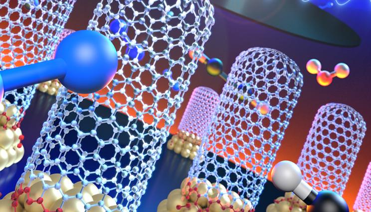
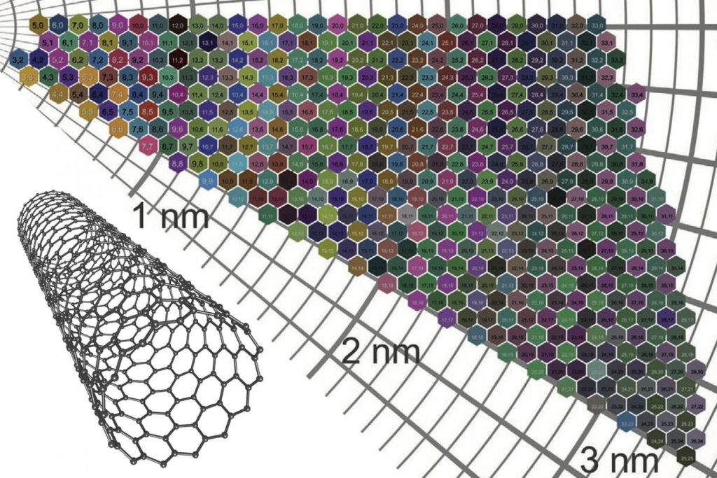
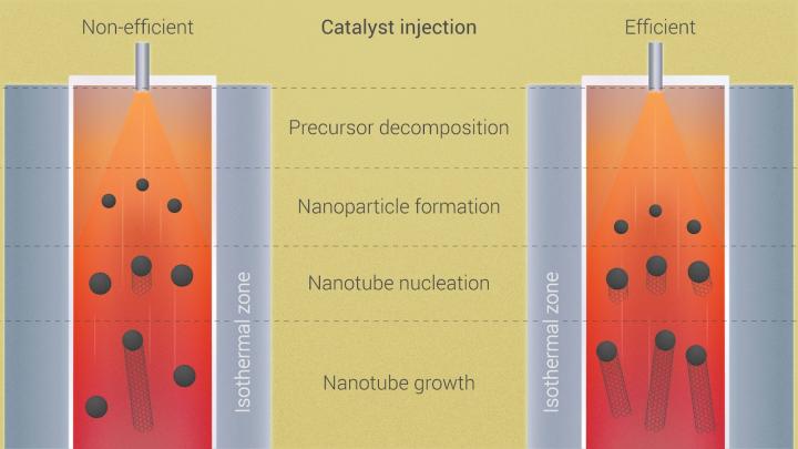
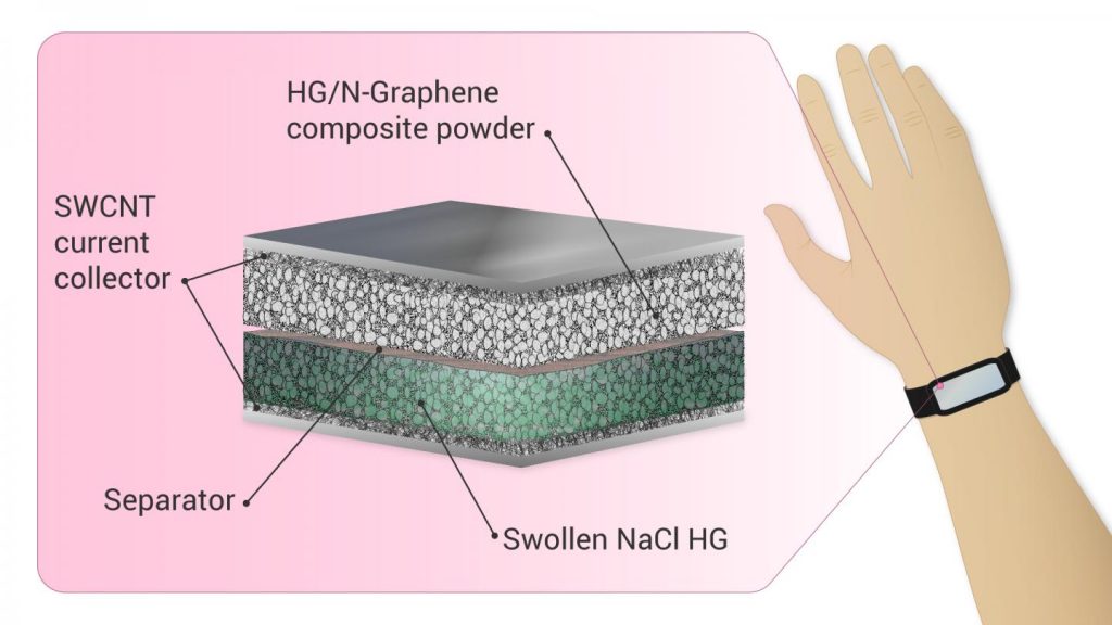
Nanotechnology, the main subject on this blog, continues to be investigated and increasingly integrated into products. You can search the ‘nanotechnology’ category here for posts of interest something I just tried. It surprises even me (I should know better) how broadly nanotechnology is researched and applied.

If you want a nice tidy list, Hamish Johnston in a December 29, 2022 posting on the Physics World Materials blog has this “Materials and nanotechnology: our favourite research in 2022,” Note: Links have been removed,

“Inherited nanobionics” makes its debut

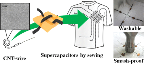
The integration of nanomaterials with living organisms is a hot topic, which is why this research on “inherited nanobionics” is on our list. Ardemis Boghossian at EPFL [École polytechnique fédérale de Lausanne] in Switzerland and colleagues have shown that certain bacteria will take up single-walled carbon nanotubes (SWCNTs). What is more, when the bacteria cells split, the SWCNTs are distributed amongst the daughter cells. The team also found that bacteria containing SWCNTs produce a significantly more electricity when illuminated with light than do bacteria without nanotubes. As a result, the technique could be used to grow living solar cells, which as well as generating clean energy, also have a negative carbon footprint when it comes to manufacturing.

Getting to back to Canada, I’m finding Saskatchewan featured more prominently here. They do a good job of promoting their science, especially the folks at the Canadian Light Source (CLS), Canada’s synchrotron, in Saskatoon. Canadian live science outreach events seeming to be coming back (slowly). Cautious organizers (who have a few dollars to spare) are also enthusiastic about hybrid events which combine online and live outreach.

After what seems like a long pause, I’m stumbling across more international news, e.g. “Nigeria and its nanotechnology research” published December 19, 2022 and “China and nanotechnology” published September 6, 2022. I think there’s also an Iran piece here somewhere.

With that …

Making resolutions in the dark

Hopefully this year I will catch up with the Council of Canadian Academies (CCA) output and finally review a few of their 2021 reports such as Leaps and Boundaries; a report on artificial intelligence applied to science inquiry and, perhaps, Powering Discovery; a report on research funding and Natural Sciences and Engineering Research Council of Canada.

Given what appears to a renewed campaign to have germline editing (gene editing which affects all of your descendants) approved in Canada, I might even reach back to a late 2020 CCA report, Research to Reality; somatic gene and engineered cell therapies. it’s not the same as germline editing but gene editing exists on a continuum.

For anyone who wants to see the CCA reports for themselves they can be found here (both in progress and completed).

I’m also going to be paying more attention to how public relations and special interests influence what science is covered and how it’s covered. In doing this 2022 roundup, I noticed that I featured an overview of fusion energy not long before the breakthrough. Indirect influence on this blog?

My post was precipitated by an article by Alex Pasternak in Fast Company. I’m wondering what precipitated Alex Pasternack’s interest in fusion energy since his self-description on the Huffington Post website states this “… focus on the intersections of science, technology, media, politics, and culture. My writing about those and other topics—transportation, design, media, architecture, environment, psychology, art, music … .”

He might simply have received a press release that stimulated his imagination and/or been approached by a communications specialist or publicists with an idea. There’s a reason for why there are so many public relations/media relations jobs and agencies.

Que sera, sera (Whatever will be, will be)

I can confidently predict that 2023 has some surprises in store. I can also confidently predict that the European Union’s big research projects (1B Euros each in funding for the Graphene Flagship and Human Brain Project over a ten year period) will sunset in 2023, ten years after they were first announced in 2013. Unless, the powers that be extend the funding past 2023.

I expect the Canadian quantum community to provide more fodder for me in the form of a 2023 report on Quantum Technologies from the Council of Canadian academies, if nothing else otherwise.

I’ve already featured these 2023 science events but just in case you missed them,

  • 2023 Preview: Bill Nye the Science Guy’s live show and Marvel Avengers S.T.A.T.I.O.N. (Scientific Training And Tactical Intelligence Operative Network) coming to Vancouver (Canada) November 24, 2022 posting
  • September 2023: Auckland, Aotearoa New Zealand set to welcome women in STEM (science, technology, engineering, and mathematics) November 15, 2022 posting

Getting back to this blog, it may not seem like a new year during the first few weeks of 2023 as I have quite the stockpile of draft posts. At this point I have drafts that are dated from June 2022 and expect to be burning through them so as not to fall further behind but will be interspersing them, occasionally, with more current posts.

Most importantly: a big thank you to everyone who drops by and reads (and sometimes even comments) on my posts!!! it’s very much appreciated and on that note: I wish you all the best for 2023.

Carbon nanotubes (CNTs) in 466 colours

Caption: A color map illustrates the inherent colors of 466 types of carbon nanotubes with unique (n,m) designations based their chiral angle and diameter. Credit: Image courtesy of Kauppinen Group/Aalto University

This is, so to speak, a new angle on carbon nanotubes (CNTs). It’s also the first time I’ve seen two universities place identical news releases on EurekAlert under their individual names.

From the Dec. 14, 2020 Rice University (US) news release or the Dec. 14, 2020 Aalto University (Finland) press release on EurekAlert,

Nanomaterials researchers in Finland, the United States and China have created a color atlas for 466 unique varieties of single-walled carbon nanotubes.

The nanotube color atlas is detailed in a study in Advanced Materials about a new method to predict the specific colors of thin films made by combining any of the 466 varieties. The research was conducted by researchers from Aalto University in Finland, Rice University and Peking University in China.

“Carbon, which we see as black, can appear transparent or take on any color of the rainbow,” said Aalto physicist Esko Kauppinen, the corresponding author of the study. “The sheet appears black if light is completely absorbed by carbon nanotubes in the sheet. If less than about half of the light is absorbed in the nanotubes, the sheet looks transparent. When the atomic structure of the nanotubes causes only certain colors of light, or wavelengths, to be absorbed, the wavelengths that are not absorbed are reflected as visible colors.”

Carbon nanotubes are long, hollow carbon molecules, similar in shape to a garden hose but with sides just one atom thick and diameters about 50,000 times smaller than a human hair. The outer walls of nanotubes are made of rolled graphene. And the wrapping angle of the graphene can vary, much like the angle of a roll of holiday gift wrap paper. If the gift wrap is rolled carefully, at zero angle, the ends of the paper will align with each side of the gift wrap tube. If the paper is wound carelessly, at an angle, the paper will overhang on one end of the tube.

The atomic structure and electronic behavior of each carbon nanotube is dictated by its wrapping angle, or chirality, and its diameter. The two traits are represented in a “(n,m)” numbering system that catalogs 466 varieties of nanotubes, each with a characteristic combination of chirality and diameter. Each (n,m) type of nanotube has a characteristic color.

Kauppinen’s research group has studied carbon nanotubes and nanotube thin films for years, and it previously succeeded in mastering the fabrication of colored nanotube thin films that appeared green, brown and silver-grey.

In the new study, Kauppinen’s team examined the relationship between the spectrum of absorbed light and the visual color of various thicknesses of dry nanotube films and developed a quantitative model that can unambiguously identify the coloration mechanism for nanotube films and predict the specific colors of films that combine tubes with different inherent colors and (n,m) designations.

Rice engineer and physicist Junichiro Kono, whose lab solved the mystery of colorful armchair nanotubes in 2012, provided films made solely of (6,5) nanotubes that were used to calibrate and verify the Aalto model. Researchers from Aalto and Peking universities used the model to calculate the absorption of the Rice film and its visual color. Experiments showed that the measured color of the film corresponded quite closely to the color forecast by the model.

The Aalto model shows that the thickness of a nanotube film, as well as the color of nanotubes it contains, affects the film’s absorption of light. Aalto’s atlas of 466 colors of nanotube films comes from combining different tubes. The research showed that the thinnest and most colorful tubes affect visible light more than those with larger diameters and faded colors.

“Esko’s group did an excellent job in theoretically explaining the colors, quantitatively, which really differentiates this work from previous studies on nanotube fluorescence and coloration,” Kono said.

Since 2013, Kono’s lab has pioneered a method for making highly ordered 2D nanotube films. Kono said he had hoped to supply Kauppinen’s team with highly ordered 2D crystalline films of nanotubes of a single chirality.

“That was the original idea, but unfortunately, we did not have appropriate single-chirality aligned films at that time,” Kono said. “In the future, our collaboration plans to extend this work to study polarization-dependent colors in highly ordered 2D crystalline films.”

The experimental method the Aalto researchers used to grow nanotubes for their films was the same as in their previous studies: Nanotubes grow from carbon monoxide gas and iron catalysts in a reactor that is heated to more than 850 degrees Celsius. The growth of nanotubes with different colors and (n,m) designations is regulated with the help of carbon dioxide that is added to the reactor.

“Since the previous study, we have pondered how we might explain the emergence of the colors of the nanotubes,” said Nan Wei, an assistant research professor at Peking University who previously worked as a postdoctoral researcher at Aalto. “Of the allotropes of carbon, graphite and charcoal are black, and pure diamonds are colorless to the human eye. However, now we noticed that single-walled carbon nanotubes can take on any color: for example, red, blue, green or brown.”

Kauppinen said colored thin films of nanotubes are pliable and ductile and could be useful in colored electronics structures and in solar cells.

“The color of a screen could be modified with the help of a tactile sensor in mobile phones, other touch screens or on top of window glass, for example,” he said.

Kauppinen said the research can also provide a foundation for new kinds of environmentally friendly dyes.

Here’s a link to and a citation for the paper,

Colors of Single‐Wall Carbon Nanotubes by Nan Wei, Ying Tian, Yongping Liao, Natsumi Komatsu, Weilu Gao, Alina Lyuleeva‐Husemann, Qiang Zhang, Aqeel Hussain, Er‐Xiong Ding, Fengrui Yao, Janne Halme. Kaihui Liu, Junichiro Kono, Hua Jiang, Esko I. Kauppinen. Advanced Materials DOI: https://doi.org/10.1002/adma.202006395 First published: 14 December 2020

Thi8s paper is open access.

Boost single-walled carbon nantube (SWCNT) production

I’m fascinated by this image,

Caption: Skoltech researchers have investigated the procedure for catalyst delivery used in the most common method of carbon nanotube production, chemical vapor deposition (CVD), offering what they call a “simple and elegant” way to boost productivity and pave the way for cheaper and more accessible nanotube-based technology. Credit: Pavel Odinev/Skoltech

If I understand it correctly, getting the catalyst particles into a tighter, more uniform formation is what could lead to a boost in the production of single-walled carbon nanotubes (SWCNTs).

The work was announced in a Nov. 30, 2020 news item in Nanowerk,

Skoltech [Skolkovo Institute of Science and Technology; Russia] researchers have investigated the procedure for catalyst delivery used in the most common method of carbon nanotube production, chemical vapor deposition (CVD), offering what they call a “simple and elegant” way to boost productivity and pave the way for cheaper and more accessible nanotube-based technology.

A Nov. 30, 2020 Skolkovo Institute of Science and Technology (Skoltech) press release (also on EurekAlert but published on Dec. 1, 2020), which originated the news item, explains in detail,

Single-walled carbon nanotubes (SWCNT), tiny rolled sheets of graphene with a thickness of just one atom, hold huge promise when it comes to applications in materials science and electronics. That is the reason why so much effort is focused on perfecting the synthesis of SWCNTs; from physical methods, such as using laser beams to ablate a graphite target, all the way to the most common CVD approach, when metal catalyst particles are used to “strip” a carbon-containing gas of its carbon and grow the nanotubes on these particles.

“The road from raw materials to carbon nanotubes requires a fine balance between dozens of reactor parameters. The formation of carbon nanotubes is a tricky and complex process that has been studied for a long time, but still keeps many secrets,” explains Albert Nasibulin, a professor at Skoltech and an adjunct professor at the Department of Chemistry and Materials Science, Aalto University School of Chemical Engineering.

Various ways of enhancing catalyst activation, in order to produce more SWCNTs with the required properties, have already been suggested. Nasibulin and his colleagues focused on the injection procedure, namely on how to distribute ferrocene vapor (a commonly used catalyst precursor) within the reactor.

They grew their carbon nanotubes using the aerosol CVD approach, using carbon monoxide as a source of carbon, and monitored the synthesis productivity and SWCNT characteristics (such as their diameter) depending on the rate of catalyst injection and the concentration of CO2 (carbon dioxide; used as an agent for fine-tuning). Ultimately the researchers concluded that “injector flow rate adjustment could lead to a 9-fold increase in the synthesis productivity while preserving most of the SWCNT characteristics”, such as their diameter, the share of defective nanotubes, and film conductivity.

“Every technology is always about efficiency. When it comes to CVD production of nanotubes, the efficiency of the catalyst is usually out of sight. However, we see a great opportunity there and this work is only a first step towards an efficient technology,” Dmitry Krasnikov, senior research scientist at Skoltech and co-author of the paper, says.

Here’s a link to and a citation for the paper,

Activation of catalyst particles for single-walled carbon nanotube synthesis by Eldar M.Khabushev, Julia V. Kolodiazhnaia, Dmitry V. Krasnikov, Albert G. Nasibulin. Chemical Engineering Journal DOI: https://doi.org/10.1016/j.cej.2020.127475 Available online 24 October 2020, 127475

This paper is behind a paywall.

New capacitor for better wearable electronics?

Supercapacitors are a predictable source of scientific interest and excitement. The latest entry in the ‘supercapacitor stakes’ is from a Russian/Finnish/US team according to a June 11, 2020 Skoltech (Skolkovo Institute of Science and Technology) press release (also on EurekAlert),

Researchers from Skoltech [Russia], Aalto University [Finland] and Massachusetts Institute of Technology [MIT; US] have designed a high-performance, low-cost, environmentally friendly, and stretchable supercapacitor that can potentially be used in wearable electronics. The paper was published in the Journal of Energy Storage.

Supercapacitors, with their high power density, fast charge-discharge rates, long cycle life, and cost-effectiveness, are a promising power source for everything from mobile and wearable electronics to electric vehicles. However, combining high energy density, safety, and eco-friendliness in one supercapacitor suitable for small devices has been rather challenging.

“Usually, organic solvents are used to increase the energy density. These are hazardous, not environmentally friendly, and they reduce the power density compared to aqueous electrolytes with higher conductivity,” says Professor Tanja Kallio from Aalto University, a co-author of the paper.

The researchers proposed a new design for a “green” and simple-to-fabricate supercapacitor. It consists of a solid-state material based on nitrogen-doped graphene flake electrodes distributed in the NaCl-containing hydrogel electrolyte. This structure is sandwiched between two single-walled carbon nanotube film current collectors, which provides stretchability. Hydrogel in the supercapacitor design enables compact packing and high energy density and allows them to use the environmentally friendly electrolyte.

The scientists managed to improve the volumetric capacitive performance, high energy density and power density for the prototype over analogous supercapacitors described in previous research. “We fabricated a prototype with unchanged performance under the 50% strain after a thousand stretching cycles. To ensure lower cost and better environmental performance, we used a NaCl-based electrolyte. Still the fabrication cost can be lowered down by implementation of 3D printing or other advanced fabrication techniques,” concluded Skoltech professor Albert Nasibulin.

Here’s a link to and a citation for the paper,

Superior environmentally friendly stretchable supercapacitor based on nitrogen-doped graphene/hydrogel and single-walled carbon nanotubes by Evgeniia Gilshtein, Cristina Flox, Farhan S.M. Ali, Bahareh Mehrabimatin, Fedor S.Fedorov, Shaoting Lin, Xuanhe Zhao, Albert G. Nasibulin, Tanja Kallio. Journal of Energy Storage Volume 30, August 2020, 101505 DOI: https://doi.org/10.1016/j.est.2020.101505

This paper is behind a paywall.

I’m trying to remember if I’ve ever before seen a material that combines graphene and single-walled carbon nanotubes (SWCNTs). Anyway, here’s an image the researchers are using illustrate their work,

Caption: This is an outline of the new supercapacitor. Credit: Pavel Odinev / Skoltech

OCSiAl becomes largest European supplier of single-walled carbon nanotubes (SWCNTs)

It’s time I posted news about OCSiAl as it’s been about five years since they were last mentioned here. An April 24, 2020 news item on AzoNano proclaims a new status for the company,

As from [sic] April 2020, OCSiAl is able to commercialize up to 100 tonnes annually of its TUBALL™ single wall carbon nanotubes [single-walled carbon nanotubes or SWCNTs] in Europe thanks to the company’s upgraded dossier under the EU’s [European Union’s] “Registration, Evaluation, Authorization and Restriction of Chemicals” (REACH) legislation, being additionally compliant with the new Annexes on nanoforms. OCSiAl will continue to expand markets for nanotubes and widen industrial applications by scaling-up its permitted volume in Australia and Canada in 2020, pending approval by the authorities.

An April 23, 2020 OCSiAl press release, which originated the news item, provides more details about the company and its customers in ‘marketingese’ (marketing language),

OCSiAl is now the only company in Europe able to commercialize up to 100 tonnes of single wall carbon nanotubes, also known as graphene nanotubes. This step allows the company to boost its presence in the region and to meet the growing market demand for industrial volumes of graphene nanotubes. The company’s current portfolio includes over 1,600 customers worldwide, with China and Europe as the two most rapidly expanding markets for nanotube applications in transportation, electronics, construction, infrastructure, renewable energy, power sources, sports equipment, 3D-printing, textiles, sensors and many more.

OCSiAl plays a leading role in improving the accessibility of information on the nature of graphene nanotubes and in forming the principles of their safe handling – the company has so far initiated 16 studies in these fields, including those required by the revised REACH annex. TUBALL nanotubes demonstrate no skin irritation, corrosion or sensitization, no mutagenic effect, and no adverse effect on reproductive toxicity. In addition, ecotoxicity studies have shown no toxic effect on Daphnia or algae. The typical exposure values of respirable fraction of TUBALL in the workplace is much less than 5% of the Recommended Exposure Limits (REL) as per NIOSH in the USA, which is of practical importance for manufacturers working with nanotubes. And end users can also be reassured that these studies have shown that no TUBALL nanotubes are released during utilization of products made with nanoaugmented materials. All these findings reflect the unique nature and morphology of TUBALL graphene nanotubes.

OCSiAl continues to accelerate the acceptance of this unique material in various markets by supplying high-quality nanotubes at an economically feasible price and in industrial volumes. TUBALL is regulated by the Environmental Protection Agency (EPA) in the US, where it is also allowed to be commercialized in industrial volumes. The company’s near-term plans include scaling-up the permitted volume of industrial commercialization of graphene nanotubes in Australia and Canada.

The company appears to be trying to rebrand carbon nanotubes as graphene nanotubes. It can be done (e.g., facial tissue instead of Kleenex or photocopy instead of Xerox) but it can take a long time and, after a brief search (May 13, 2020), I was not able to find any other reference to ‘graphene nanotubes’ online.

Between the two of them, OCSiAl’s Wikipedia entry and the company’s Team webpage (scroll down past the smiling faces), you can find some company history.

Purifying carbon nanotubes with dietary fiber

This work comes out of Japan according to a November 2, 2019 news item on Nanowerk,

A new, cheaper method easily and effectively separates two types of carbon nanotubes. The process, developed by Nagoya University researchers in Japan, could be up-scaled for manufacturing purified batches of single-wall carbon nanotubes that can be used in high-performance electronic devices.

Single-wall carbon nanotubes (SWCNTs) have excellent electronic and mechanical properties, making them ideal candidates for use in a wide range of electronic devices, including the thin-film transistors found in LCD displays. A problem is that only two-thirds of manufactured SWCNTs are suitable for use in electronic devices. The useful semiconducting SWCNTs must be separated from the unwanted metallic ones. But the most powerful purification process, known as aqueous two-phase extraction, currently involves the use of a costly polysaccharide, called dextran.

Caption: The unwanted metallic SWCNTs deposited at the bottom of the solution, while the wanted semiconducting ones floated to the top. Credit: Haruka Omachi

An October 29, 2019 Nagoya University press release (also on EurekAlert but dated Nov. 2, 2019), which originated the news item, describes how dextran could be replaced with something much cheaper in the SWCNT purification process,

Organic chemist Haruka Omachi and colleagues at Nagoya University hypothesized that dextran’s effectiveness in separating semiconducting from metallic SWCNTs lies in the linkages connecting its glucose units. Instead of using dextran to separate the two types of SWCNTs, the team tried the significantly cheaper isomaltodextran, which has many more of these linkages.

A batch of SWCNTs was left for 15 minutes in a solution containing polyethylene glycol and isomaltodextrin and then centrifuged for five minutes. Three different types of isomaltodextrin were tried, each with a different number of linkages and a different molecular weight. The team found that metallic SWCNTs separated to the bottom isomaltodextrin part of the solution, while the semiconducting SWCNTs floated to the top polyethylene glycol part.

The type of isomaltodextrin with high molecular weight and the most linkages was the most (99%) effective in separating the two types of SWCNTs. The team also found that another polysaccharide, called pullulan, whose glucose units are connected with different kinds of linkages, was ineffective in separating the two types of SWCNTs. The researchers suggest that the number and type of linkages present in isomaltodextrin play an important role in their ability to effectively separate the carbon nanotubes.

The team also found that a thin-film transistor made with their purified semiconducting SWCNTs performed very well.

Isomaltodextrin is a cheap and widely available polysaccharide produced from starch that is used as a dietary fibre. This makes it a cost-effective alternative for the SWCNT extraction process. Omachi and his colleagues are currently in discussions with companies to commercialize their approach. They are also working on improving the performance of thin-film transistors using semiconducting SWCNTs in flexible displays and sensor devices.

Here’s a link to and a citation for the paper,

Aqueous two-phase extraction of semiconducting single-wall carbon nanotubes with isomaltodextrin and thin-film transistor applications by Haruka Omachi, Tomohiko Komuro, Kaisei Matsumoto, Minako Nakajima, Hikaru Watanabe, Jun Hirotani, Yutaka Ohno, and Hisanori Shinohara. Applied Physics Express, Volume 12, Number 9 DOI: https://doi.org/10.7567/1882-0786/ab369 Published 14 August 2019 • © 2019 The Japan Society of Applied Physics

This paper is open access.

Double-walled carbon nanotubes have superior electrical properties?

A March 27, 2020 news item on Nanowerk suggests that double-walled carbon nanotubes (DWCNTs) may offer some advantages over single-walled carbon nanotubes (SWCNTs), NOTE: A link has been removed,

One nanotube could be great for electronics applications, but there’s new evidence that two could be tops.

Rice University engineers already knew that size matters when using single-walled carbon nanotubes for their electrical properties. But until now, nobody had studied how electrons act when confronted with the Russian doll-like structure of multiwalled tubes.

There’s a diagram representing the work,

Caption: Rice University theorists have calculated flexoelectric effects in double-walled carbon nanotubes. The electrical potential (P) of atoms on either side of a graphene sheet (top) are identical, but not when the sheet is curved into a nanotube. Double-walled nanotubes (bottom) show unique effects as band gaps in inner and outer tubes are staggered. Credit: Yakobson Research Group/Rice University

A March 27, 2020 Rice University news release (also on EurekAlert), which originated the news item, delves further (NOTE: Links have been removed),

The Rice lab of materials theorist Boris Yakobson has now calculated the impact of curvature of semiconducting double-wall carbon nanotubes on their flexoelectric voltage, a measure of electrical imbalance between the nanotube’s inner and outer walls.

This affects how suitable nested nanotube pairs may be for nanoelectronics applications, especially photovoltaics.

The theoretical research by Yakobson’s Brown School of Engineering group appears in the American Chemical Society journal Nano Letters.

In an 2002 study, Yakobson and his Rice colleagues had revealed how charge transfer, the difference between positive and negative poles that allows voltage to exist between one and the other, scales linearly to the curvature of the nanotube wall. The width of the tube dictates curvature, and the lab found that the thinner the nanotube (and thus larger the curvature), the greater the potential voltage.

When carbon atoms form flat graphene, the charge density of the atoms on either side of the plane are identical, Yakobson said. Curving the graphene sheet into a tube breaks that symmetry, changing the balance.

That creates a flexoelectric local dipole in the direction of, and proportional to, the curvature, according to the researchers, who noted that the flexoelectricity of 2D carbon “is a remarkable but also fairly subtle effect.”

But more than one wall greatly complicates the balance, altering the distribution of electrons. In double-walled nanotubes, the curvature of the inner and outer tubes differ, giving each a distinct band gap. Additionally, the models showed the flexoelectric voltage of the outer wall shifts the band gap of the inner wall, creating a staggered band alignment in the nested system.

“The novelty is that the inserted tube, the ‘baby’ (inside) matryoshka has all of its quantum energy levels shifted because of the voltage created by exterior nanotube,” Yakobson said. The interplay of different curvatures, he said, causes a straddling-to-staggered band gap transition that takes place at an estimated critical diameter of about 2.4 nanometers.

“This is a huge advantage for solar cells, essentially a prerequisite for separating positive and negative charges to create a current,” Yakobson said. “When light is absorbed, an electron always jumps from the top of an occupied valence band (leaving a ‘plus’ hole behind) to the lowest state of empty conductance band.

“But in a staggered configuration they happen to be in different tubes, or layers,” he said. “The ‘plus’ and ‘minus’ get separated between the tubes and can flow away by generating current in a circuit.”

The team’s calculations also showed that modifying the nanotubes’ surfaces with either positive or negative atoms could create “substantial voltages of either sign” up to three volts. “Although functionalization could strongly perturb the electronic properties of nanotubes, it may be a very powerful way of inducing voltage for certain applications,” the researchers wrote.

The team suggested its findings may apply to other types of nanotubes, including boron nitride and molybdenum disulfide, on their own or as hybrids with carbon nanotubes.

Here’s a link to and a citation for the paper,

Flexoelectricity and charge separation in carbon nanotubes by Vasilii I. Artyukhov, Sunny Gupta, Alex Kutana, Boris I. Yakobson. Nano Lett. 2020, XXXX, XXX, XXX-XXX DOI: https://doi.org/10.1021/acs.nanolett.9b05345 [Online] Publication Date:March 10, 2020 Copyright © 2020 American Chemical Society

This paper is behind a paywall.

Wearable electronic textiles from the UK, India, and Canada: two different carbon materials

It seems wearable electronic textiles may be getting nearer to the marketplace. I have three research items (two teams working with graphene and one working with carbon nanotubes) that appeared on my various feeds within two days of each other.

UK/China

This research study is the result of a collaboration between UK and Chinese scientists. From a May 15, 2019 news item on phys.org (Note: Links have been removed),


Wearable electronic components incorporated directly into fabrics have been developed by researchers at the University of Cambridge. The devices could be used for flexible circuits, healthcare monitoring, energy conversion, and other applications.

The Cambridge researchers, working in collaboration with colleagues at Jiangnan University in China, have shown how graphene – a two-dimensional form of carbon – and other related materials can be directly incorporated into fabrics to produce charge storage elements such as capacitors, paving the way to textile-based power supplies which are washable, flexible and comfortable to wear.

The research, published in the journal Nanoscale, demonstrates that graphene inks can be used in textiles able to store electrical charge and release it when required. The new textile electronic devices are based on low-cost, sustainable and scalable dyeing of polyester fabric. The inks are produced by standard solution processing techniques.

Building on previous work by the same team, the researchers designed inks which can be directly coated onto a polyester fabric in a simple dyeing process. The versatility of the process allows various types of electronic components to be incorporated into the fabric.

Schematic of the textile-based capacitor integrating GNP/polyesters as electrodes and h-BN/polyesters as dielectrics. Credit: Felice Torrisi

A May 16, 2019 University of Cambridge press release, which originated the news item, probes further,

Most other wearable electronics rely on rigid electronic components mounted on plastic or textiles. These offer limited compatibility with the skin in many circumstances, are damaged when washed and are uncomfortable to wear because they are not breathable.

“Other techniques to incorporate electronic components directly into textiles are expensive to produce and usually require toxic solvents, which makes them unsuitable to be worn,” said Dr Felice Torrisi from the Cambridge Graphene Centre, and the paper’s corresponding author. “Our inks are cheap, safe and environmentally-friendly, and can be combined to create electronic circuits by simply overlaying different fabrics made of two-dimensional materials on the fabric.”

The researchers suspended individual graphene sheets in a low boiling point solvent, which is easily removed after deposition on the fabric, resulting in a thin and uniform conducting network made up of multiple graphene sheets. The subsequent overlay of several graphene and hexagonal boron nitride (h-BN) fabrics creates an active region, which enables charge storage. This sort of ‘battery’ on fabric is bendable and can withstand washing cycles in a normal washing machine.

“Textile dyeing has been around for centuries using simple pigments, but our result demonstrates for the first time that inks based on graphene and related materials can be used to produce textiles that could store and release energy,” said co-author Professor Chaoxia Wang from Jiangnan University in China. “Our process is scalable and there are no fundamental obstacles to the technological development of wearable electronic devices both in terms of their complexity and performance.”

The work done by the Cambridge researchers opens a number of commercial opportunities for ink based on two-dimensional materials, ranging from personal health and well-being technology, to wearable energy and data storage, military garments, wearable computing and fashion.

“Turning textiles into functional energy storage elements can open up an entirely new set of applications, from body-energy harvesting and storage to the Internet of Things,” said Torrisi “In the future our clothes could incorporate these textile-based charge storage elements and power wearable textile devices.”

Here’s a link to and a citation for the paper,

Wearable solid-state capacitors based on two-dimensional material all-textile heterostructures by Siyu Qiang, Tian Carey, Adrees Arbab, Weihua Song, Chaoxia Wang and Felice Torris. Nanoscale, 2019, Advance Article DOI: 10.1039/C9NR00463G First published on 18 Apr 2019

This paper is behind a paywall.

India

Prior to graphene’s reign as the ‘it’ carbon material, carbon nanotubes (CNTs) ruled. It’s been quieter on the CNT front since graphene took over but a May 15, 2019 Nanowerk Spotlight article by Michael Berger highlights some of the latest CNT research coming out of India,


The most important technical challenge is to blend the chemical nature of raw materials with fabrication techniques and processability, all of which are diametrically conflicting for textiles and conventional energy storage devices. A team from Indian Institute of Technology Bombay has come out with a comprehensive approach involving simple and facile steps to fabricate a wearable energy storage device. Several scientific and technological challenges were overcome during this process.

First, to achieve user-comfort and computability with clothing, the scaffold employed was the the same as what a regular fabric is made up of – cellulose fibers. However, cotton yarns are electrical insulators and therefore practically useless for any electronics. Therefore, the yarns are coated with single-wall carbon nanotubes (SWNTs).

SWNTs are hollow, cylindrical allotropes of carbon and combine excellent mechanical strength with electrical conductivity and surface area. Such a coating converts the electrical insulating cotton yarn to a metallic conductor with high specific surface area. At the same time, using carbon-based materials ensures that the final material remains light-weight and does not cause user discomfort that can arise from metallic wires such as copper and gold. This CNT-coated cotton yarn (CNT-wires) forms the electrode for the energy storage device.

Next, the electrolyte is composed of solid-state electrolyte sheets since no liquid-state electrolytes can be used for this purpose. However, solid state electrolytes suffer from poor ionic conductivity – a major disadvantage for energy storage applications. Therefore, a steam-based infiltration approach that enhances the ionic conductivity of the electrolyte is adopted. Such enhancement of humidity significantly increases the energy storage capacity of the device.


The integration of the CNT-wire electrode with the electrolyte sheet was carried out by a simple and elegant approach of interweaving the CNT-wire through the electrolyte (see Figure 1). This resulted in cross-intersections which are actually junctions where the electrical energy can be stored. Each such junction is now an energy storage unit, referred to as sewcap.

The advantage of this process is that several 100s and 1000s of sewcaps can be made in a small area and integrated to increase the total amount of energy stored in the system. This scalability is unique and critical aspect of this work and stems from the approach of interweaving.

Further, this process is completely adaptable with current processes used in textile industries. Hence, a proportionately large energy-storage is achieved by creating sewcap-junctions in various combinations.

All components of the final sewcap device are flexible. However, they need to be protected from environmental effects such as temperature, humidity and sweat while retaining the mechanical flexibility. This is achieved by laminating the entire device between polymer sheets. The process is exactly similar to the one used for protecting documents and ID cards.

The laminated sewcap can be integrated easily on clothing and fabrics while retaining the flexibility and sturdiness. This is demonstrated by the unchanged performance of the device during extreme and harsh mechanical testing such as striking repeatedly with a hammer, complete flexing, bending and rolling and washing in a laundry machine.

In fact, this is the first device that has been proven to be stable under rigorous washing conditions in the presence of hot water, detergents and high torque (spinning action of washing machine). This provides the device with comprehensive mechanical stability.


CNTs have high surface area and electrical conductivity. The CNT-wire combines these properties of CNTs with stability and porosity of cellulose yarns. The junction created by interweaving is essentially comprised of two such CNT-wires that are sandwiching an electrolyte. Application of potential difference leads to polarization of the electrolyte thus enabling energy storage similar to the way in which a conventional capacitor acts.

“We use the advantage of the interweaving process and create several such junctions. So, with each junction being able to store a certain amount of electrical energy, all the junctions synchronized are able to store a large amount of energy. This provides high energy density to the device,” Prof. C. Subramaniam, Department of Chemistry, IIT Bombay and corresponding author of the paper points out.

The device has also been employed for lighting up an LED [light-emitting diode]. This can be potentially scaled to provide electrical energy demanded by the application.

This image accompanies the paper written by Prof. C. Subramaniam and his team,

Courtesy: IACS Applied Materials Interfaces

Here’s a link to and a citation for the paper,

Interwoven Carbon Nanotube Wires for High-Performing, Mechanically Robust, Washable, and Wearable Supercapacitors by Mihir Kumar Jha, Kenji Hata, and Chandramouli Subramaniam. ACS Appl. Mater. Interfaces, Article ASAP DOI: 10.1021/acsami.8b22233 Publication Date (Web): April 29, 2019 Copyright © 2019 American Chemical Society

This paper is behind a paywall.

Canada

A research team from the University of British Columbia (UBC at the Okanagan Campus) joined the pack with a May 16, 2019 news item on ScienceDaily,

Forget the smart watch. Bring on the smart shirt.

Researchers at UBC Okanagan’s School of Engineering have developed a low-cost sensor that can be interlaced into textiles and composite materials. While the research is still new, the sensor may pave the way for smart clothing that can monitor human movement.

A May 16, 2019 UBC news release (also on EurekAlert), which originated the news item, describes the work in more detail,


“Microscopic sensors are changing the way we monitor machines and humans,” says Hoorfar, lead researcher at the Advanced Thermo-Fluidic Lab at UBC’s Okanagan campus. “Combining the shrinking of technology along with improved accuracy, the future is very bright in this area.”

This ‘shrinking technology’ uses a phenomenon called piezo-resistivity—an electromechanical response of a material when it is under strain. These tiny sensors have shown a great promise in detecting human movements and can be used for heart rate monitoring or temperature control, explains Hoorfar.

Her research, conducted in partnership with UBC Okanagan’s Materials and Manufacturing Research Institute, shows the potential of a low-cost, sensitive and stretchable yarn sensor. The sensor can be woven into spandex material and then wrapped into a stretchable silicone sheath. This sheath protects the conductive layer against harsh conditions and allows for the creation of washable wearable sensors.

While the idea of smart clothing—fabrics that can tell the user when to hydrate, or when to rest—may change the athletics industry, UBC Professor Abbas Milani says the sensor has other uses. It can monitor deformations in fibre-reinforced composite fabrics currently used in advanced industries such as automotive, aerospace and marine manufacturing.

The low-cost stretchable composite sensor has also shown a high sensitivity and can detect small deformations such as yarn stretching as well as out-of-plane deformations at inaccessible places within composite laminates, says Milani, director of the UBC Materials and Manufacturing Research Institute.

The testing indicates that further improvements in its accuracy could be achieved by fine-tuning the sensor’s material blend and improving its electrical conductivity and sensitivity This can eventually make it able to capture major flaws like “fibre wrinkling” during the manufacturing of advanced composite structures such as those currently used in airplanes or car bodies.

“Advanced textile composite materials make the most of combining the strengths of different reinforcement materials and patterns with different resin options,” he says. “Integrating sensor technologies like piezo-resistive sensors made of flexible materials compatible with the host textile reinforcement is becoming a real game-changer in the emerging era of smart manufacturing and current automated industry trends.”

Here’s a link to and a citation for the paper,

Graphene‐Coated Spandex Sensors Embedded into Silicone Sheath for Composites Health Monitoring and Wearable Applications by Hossein Montazerian, Armin Rashidi, Arash Dalili, Homayoun Najjaran, Abbas S. Milani, Mina Hoorfar. Small Volume15, Issue17 April 26, 2019 1804991 DOI: https://doi.org/10.1002/smll.201804991 First published: 28 March 2019

This paper is behind a paywall.

Will there be one winner or will they find CNTs better for one type of wearable tech textile while graphene excels for another type of wearable tech textile?