Monthly Archives: March 2017

The inside scoop on beetle exoskeletons

In the past I’ve covered work on the Namib beetle and its bumps which allow it to access condensation from the air in one of the hottest places on earth and work on jewel beetles and how their structural colo(u)r is derived. Now, there’s research into a beetle’s body armor from the University of Nebraska-Lincoln according to a Feb. 22, 2017 news item on ScienceDaily,

Beetles wear a body armor that should weigh them down — think medieval knights and turtles. In fact, those hard shells protecting delicate wings are surprisingly light, allowing even flight.

Better understanding the structure and properties of beetle exoskeletons could help scientists engineer lighter, stronger materials. Such materials could, for example, reduce gas-guzzling drag in vehicles and airplanes and reduce the weight of armor, lightening the load for the 21st-century knight.

But revealing exoskeleton architecture at the nanoscale has proven difficult. Nebraska’s Ruiguo Yang, assistant professor of mechanical and materials engineering, and his colleagues found a way to analyze the fibrous nanostructure. …

A Feb. 22, 2017 University of Nebraska-Lincoln news release by Gillian Klucas (also on EurekAlert), which originated the news item, describes skeletons and the work in more detail,

The lightweight exoskeleton is composed of chitin fibers just around 20 nanometers in diameter (a human hair measures approximately 75,000 nanometers in diameter) and packed and piled into layers that twist in a spiral, like a spiral staircase. The small diameter and helical twisting, known as Bouligand, make the structure difficult to analyze.

Yang and his team developed a method of slicing down the spiral to reveal a surface of cross-sections of fibers at different orientations. From that viewpoint, the researchers were able to analyze the fibers’ mechanical properties with the aid of an atomic force microscope. This type of microscope applies a tiny force to a test sample, deforms the sample and monitors the sample’s response. Combining the experimental procedure and theoretical analysis, the researchers were able to reveal the nanoscale architecture of the exoskeleton and the material properties of the nanofibers.

Yang holds a piece of the atomic force microscope used to measure the beetle's surface. A small wire can barely be seen in the middle of the piece. Unseen is a two-nano-size probe attached to the wire, which does the actual measuring.

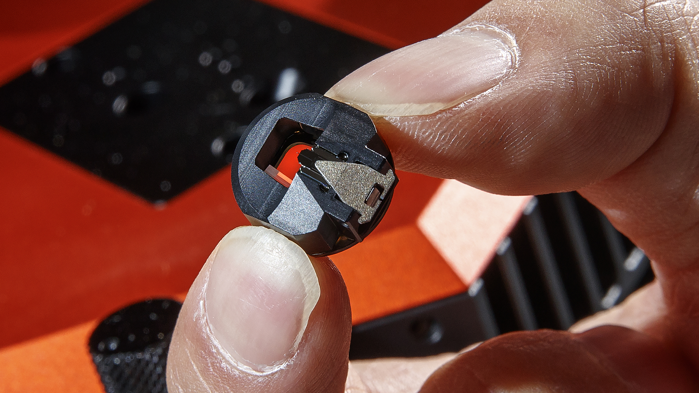
Craig Chandler | University Communication

Yang holds a piece of the atomic force microscope used to measure the beetle’s surface. A small wire can barely be seen in the middle of the piece. Unseen is a two-nano-size probe attached to the wire, which does the actual measuring.

They made their discoveries in the common figeater beetle, Cotinis mutabilis, a metallic green native of the western United States. But the technique can be used on other beetles and hard-shelled creatures and might also extend to artificial materials with fibrous structures, Yang said.

Comparing beetles with differing demands on their exoskeletons, such as defending against predators or environmental damage, could lead to evolutionary insights as well as a better understanding of the relationship between structural features and their properties.

Yang’s co-authors are Alireza Zaheri and Horacio Espinosa of Northwestern University; Wei Gao of the University of Texas at San Antonio; and Cheryl Hayashi of the University of California, Riverside.

Here’s a link to and a citation for the paper,

Exoskeletons: AFM Identification of Beetle Exocuticle: Bouligand Structure and Nanofiber Anisotropic Elastic Properties by Ruiguo Yang, Alireza Zaheri,Wei Gao, Charely Hayashi, Horacio D. Espinosa. Adv. Funct. Mater. vol. 27 (6) 2017 DOI: 10.1002/adfm.201770031 First published: 8 February 2017

This paper is behind a paywall.

The Imagineers of War: The Untold Story of DARPA, the Pentagon Agency That Changed the World on March 21, 2017 at the Woodrow Wilson International Center for Scholars

I received a March 17, 2017 Woodrow Wilson International Center for Scholars notice (via email) about this upcoming event,

The Imagineers of War: The Untold Story of DARPA [Defense Advanced Research Projects Agency], the Pentagon Agency That Changed the World

There will be a webcast of this event

In The Imagineers of War, Weinberger gives us a definitive history of the agency that has quietly shaped war and technology for nearly 60 years. Founded in 1958 in response to the launch of Sputnik, DARPA’s original mission was to create “the unimagined weapons of the future.” Over the decades, DARPA has been responsible for countless inventions and technologies that extend well beyond military technology.

Weinberger has interviewed more than one hundred former Pentagon officials and scientists involved in DARPA’s projects—many of whom have never spoken publicly about their work with the agency—and pored over countless declassified records from archives around the country, documents obtained under the Freedom of Information Act, and exclusive materials provided by sources. The Imagineers of War is a compelling and groundbreaking history in which science, technology, and politics collide.

Speakers


  • Sharon Weinberger

    Global Fellow
    Author, Imagineers of War, National Security Editor at The Intercept and former Wilson Center Fellow

  • Richard Whittle

    Global Fellow
    Author, Predator: The Secret Origins of the Drone Revolution and Wilson Center Global Fellow

The logistics:

6th Floor, Woodrow Wilson Center

I first heard about DARPA in reference to the internet. A developer I was working with noted that ARPA (DARPA’s predecessor agency) was instrumental in the development of the internet.

You can register for the event here. Should you be interested in the webcast, you can check this page.

As a point of interest, the Wilson Center (also known as the Woodrow Wilson International Center for Scholars) is one of the independent agencies slated to be defunded in the 2017 US budget as proposed by President Donald Trump according to a March 16, 2017 article by Elaine Godfrey for The Atlantic.

Atomic force microscope (AFM) shrunk down to a dime-sized device?

Before getting to the announcement, here’s a little background from Dexter Johnson’s Feb. 21, 2017 posting on his NanoClast blog (on the IEEE [Institute of Electrical and Electronics Engineers] website; Note: Links have been removed),

Ever since the 1980s, when Gerd Binnig of IBM first heard that “beautiful noise” made by the tip of the first scanning tunneling microscope (STM) dragging across the surface of an atom, and he later developed the atomic force microscope (AFM), these microscopy tools have been the bedrock of nanotechnology research and development.

AFMs have continued to evolve over the years, and at one time, IBM even looked into using them as the basis of a memory technology in the company’s Millipede project. Despite all this development, AFMs have remained bulky and expensive devices, costing as much as $50,000 [or more].

Now, here’s the announcement in a Feb. 15, 2017 news item on Nanowerk,

Researchers at The University of Texas at Dallas have created an atomic force microscope on a chip, dramatically shrinking the size — and, hopefully, the price tag — of a high-tech device commonly used to characterize material properties.

“A standard atomic force microscope is a large, bulky instrument, with multiple control loops, electronics and amplifiers,” said Dr. Reza Moheimani, professor of mechanical engineering at UT Dallas. “We have managed to miniaturize all of the electromechanical components down onto a single small chip.”

A Feb. 15, 2017 University of Texas at Dallas news release, which originated the news item, provides more detail,

An atomic force microscope (AFM) is a scientific tool that is used to create detailed three-dimensional images of the surfaces of materials, down to the nanometer scale — that’s roughly on the scale of individual molecules.

The basic AFM design consists of a tiny cantilever, or arm, that has a sharp tip attached to one end. As the apparatus scans back and forth across the surface of a sample, or the sample moves under it, the interactive forces between the sample and the tip cause the cantilever to move up and down as the tip follows the contours of the surface. Those movements are then translated into an image.

“An AFM is a microscope that ‘sees’ a surface kind of the way a visually impaired person might, by touching. You can get a resolution that is well beyond what an optical microscope can achieve,” said Moheimani, who holds the James Von Ehr Distinguished Chair in Science and Technology in the Erik Jonsson School of Engineering and Computer Science. “It can capture features that are very, very small.”

The UT Dallas team created its prototype on-chip AFM using a microelectromechanical systems (MEMS) approach.

“A classic example of MEMS technology are the accelerometers and gyroscopes found in smartphones,” said Dr. Anthony Fowler, a research scientist in Moheimani’s Laboratory for Dynamics and Control of Nanosystems and one of the article’s co-authors. “These used to be big, expensive, mechanical devices, but using MEMS technology, accelerometers have shrunk down onto a single chip, which can be manufactured for just a few dollars apiece.”

The MEMS-based AFM is about 1 square centimeter in size, or a little smaller than a dime. It is attached to a small printed circuit board, about half the size of a credit card, which contains circuitry, sensors and other miniaturized components that control the movement and other aspects of the device.

Conventional AFMs operate in various modes. Some map out a sample’s features by maintaining a constant force as the probe tip drags across the surface, while others do so by maintaining a constant distance between the two.

“The problem with using a constant height approach is that the tip is applying varying forces on a sample all the time, which can damage a sample that is very soft,” Fowler said. “Or, if you are scanning a very hard surface, you could wear down the tip,”

The MEMS-based AFM operates in “tapping mode,” which means the cantilever and tip oscillate up and down perpendicular to the sample, and the tip alternately contacts then lifts off from the surface. As the probe moves back and forth across a sample material, a feedback loop maintains the height of that oscillation, ultimately creating an image.

“In tapping mode, as the oscillating cantilever moves across the surface topography, the amplitude of the oscillation wants to change as it interacts with sample,” said Dr. Mohammad Maroufi, a research associate in mechanical engineering and co-author of the paper. “This device creates an image by maintaining the amplitude of oscillation.”

Because conventional AFMs require lasers and other large components to operate, their use can be limited. They’re also expensive.

“An educational version can cost about $30,000 or $40,000, and a laboratory-level AFM can run $500,000 or more,” Moheimani said. “Our MEMS approach to AFM design has the potential to significantly reduce the complexity and cost of the instrument.

“One of the attractive aspects about MEMS is that you can mass produce them, building hundreds or thousands of them in one shot, so the price of each chip would only be a few dollars. As a result, you might be able to offer the whole miniature AFM system for a few thousand dollars.”

A reduced size and price tag also could expand the AFMs’ utility beyond current scientific applications.

“For example, the semiconductor industry might benefit from these small devices, in particular companies that manufacture the silicon wafers from which computer chips are made,” Moheimani said. “With our technology, you might have an array of AFMs to characterize the wafer’s surface to find micro-faults before the product is shipped out.”

The lab prototype is a first-generation device, Moheimani said, and the group is already working on ways to improve and streamline the fabrication of the device.

“This is one of those technologies where, as they say, ‘If you build it, they will come.’ We anticipate finding many applications as the technology matures,” Moheimani said.

In addition to the UT Dallas researchers, Michael Ruppert, a visiting graduate student from the University of Newcastle in Australia, was a co-author of the journal article. Moheimani was Ruppert’s doctoral advisor.

So, an AFM that could cost as much as $500,000 for a laboratory has been shrunk to this size and become far less expensive,

A MEMS-based atomic force microscope developed by engineers at UT Dallas is about 1 square centimeter in size (top center). Here it is attached to a small printed circuit board that contains circuitry, sensors and other miniaturized components that control the movement and other aspects of the device. Courtesy: University of Texas at Dallas

Of course, there’s still more work to be done as you’ll note when reading Dexter’s Feb. 21, 2017 posting where he features answers to questions he directed to the researchers.

Here’s a link to and a citation for the paper,

On-Chip Dynamic Mode Atomic Force Microscopy: A Silicon-on-Insulator MEMS Approach by  Michael G. Ruppert, Anthony G. Fowler, Mohammad Maroufi, S. O. Reza Moheimani. IEEE Journal of Microelectromechanical Systems Volume: 26 Issue: 1  Feb. 2017 DOI: 10.1109/JMEMS.2016.2628890 Date of Publication: 06 December 2016

This paper is behind a paywall.

A DNA switch for new electronic applications

I little dreamed when reading “The Double Helix : A Personal Account of the Discovery of the Structure of DNA” by James Watson that DNA (deoxyribonucleic acid) would one day become just another material for scientists to manipulate. A Feb. 20, 2017 news item on ScienceDaily describes the use of DNA as a material in electronics applications,

DNA, the stuff of life, may very well also pack quite the jolt for engineers trying to advance the development of tiny, low-cost electronic devices.

Much like flipping your light switch at home — only on a scale 1,000 times smaller than a human hair — an ASU [Arizona State University]-led team has now developed the first controllable DNA switch to regulate the flow of electricity within a single, atomic-sized molecule. The new study, led by ASU Biodesign Institute researcher Nongjian Tao, was published in the advanced online journal Nature Communications.

DNA, the stuff of life, may very well also pack quite the jolt for engineers trying to advance the development of tiny, low-cost electronic devices. Courtesy: ASU

A Feb. 20, 2017 ASU news release (also on EurekAlert), which originated the news item, provides more detail,

“It has been established that charge transport is possible in DNA, but for a useful device, one wants to be able to turn the charge transport on and off. We achieved this goal by chemically modifying DNA,” said Tao, who directs the Biodesign Center for Bioelectronics and Biosensors and is a professor in the Fulton Schools of Engineering. “Not only that, but we can also adapt the modified DNA as a probe to measure reactions at the single-molecule level. This provides a unique way for studying important reactions implicated in disease, or photosynthesis reactions for novel renewable energy applications.”

Engineers often think of electricity like water, and the research team’s new DNA switch acts to control the flow of electrons on and off, just like water coming out of a faucet.

Previously, Tao’s research group had made several discoveries to understand and manipulate DNA to more finely tune the flow of electricity through it. They found they could make DNA behave in different ways — and could cajole electrons to flow like waves according to quantum mechanics, or “hop” like rabbits in the way electricity in a copper wire works —creating an exciting new avenue for DNA-based, nano-electronic applications.

Tao assembled a multidisciplinary team for the project, including ASU postdoctoral student Limin Xiang and Li Yueqi performing bench experiments, Julio Palma working on the theoretical framework, with further help and oversight from collaborators Vladimiro Mujica (ASU) and Mark Ratner (Northwestern University).

To accomplish their engineering feat, Tao’s group, modified just one of DNA’s iconic double helix chemical letters, abbreviated as A, C, T or G, with another chemical group, called anthraquinone (Aq). Anthraquinone is a three-ringed carbon structure that can be inserted in between DNA base pairs but contains what chemists call a redox group (short for reduction, or gaining electrons or oxidation, losing electrons).

These chemical groups are also the foundation for how our bodies’ convert chemical energy through switches that send all of the electrical pulses in our brains, our hearts and communicate signals within every cell that may be implicated in the most prevalent diseases.

The modified Aq-DNA helix could now help it perform the switch, slipping comfortably in between the rungs that make up the ladder of the DNA helix, and bestowing it with a new found ability to reversibly gain or lose electrons.

Through their studies, when they sandwiched the DNA between a pair of electrodes, they careful [sic] controlled their electrical field and measured the ability of the modified DNA to conduct electricity. This was performed using a staple of nano-electronics, a scanning tunneling microscope, which acts like the tip of an electrode to complete a connection, being repeatedly pulled in and out of contact with the DNA molecules in the solution like a finger touching a water droplet.

“We found the electron transport mechanism in the present anthraquinone-DNA system favors electron “hopping” via anthraquinone and stacked DNA bases,” said Tao. In addition, they found they could reversibly control the conductance states to make the DNA switch on (high-conductance) or switch-off (low conductance). When anthraquinone has gained the most electrons (its most-reduced state), it is far more conductive, and the team finely mapped out a 3-D picture to account for how anthraquinone controlled the electrical state of the DNA.

For their next project, they hope to extend their studies to get one step closer toward making DNA nano-devices a reality.

“We are particularly excited that the engineered DNA provides a nice tool to examine redox reaction kinetics, and thermodynamics the single molecule level,” said Tao.

Here’s a link to and a citation for the paper,

I last featured Tao’s work with DNA in an April 20, 2015 posting.

Gate-controlled conductance switching in DNA by Limin Xiang, Julio L. Palma, Yueqi Li, Vladimiro Mujica, Mark A. Ratner, & Nongjian Tao.  Nature Communications 8, Article number: 14471 (2017)  doi:10.1038/ncomms14471 Published online: 20 February 2017

This paper is open access.

CRISPR patent decision: Harvard’s and MIT’s Broad Institute victorious—for now

I have written about the CRISPR patent tussle (Harvard & MIT’s [Massachusetts Institute of Technology] Broad Institute vs the University of California at Berkeley) previously in a Jan. 6, 2015 posting and in a more detailed May 14, 2015 posting. I also mentioned (in a Jan. 17, 2017 posting) CRISPR and its patent issues in the context of a posting about a Slate.com series on Frankenstein and the novel’s applicability to our own time. This patent fight is being bitterly fought as fortunes are at stake.

It seems a decision has been made regarding the CRISPR patent claims. From a Feb. 17, 2017 article by Charmaine Distor for The Science Times,

After an intense court battle, the US Patent and Trademark Office (USPTO) released its ruling on February 15 [2017]. The rights for the CRISPR-Cas9 gene editing technology was handed over to the Broad Institute of Harvard University and the Massachusetts Institute of Technology (MIT).

According to an article in Nature, the said court battle was between the Broad Institute and the University of California. The two institutions are fighting over the intellectual property right for the CRISPR patent. The case between the two started when the patent was first awarded to the Broad Institute despite having the University of California apply first for the CRISPR patent.

Heidi Ledford’s Feb. 17, 2017 article for Nature provides more insight into the situation (Note: Links have been removed),

It [USPTO] ruled that the Broad Institute of Harvard and MIT in Cambridge could keep its patents on using CRISPR–Cas9 in eukaryotic cells. That was a blow to the University of California in Berkeley, which had filed its own patents and had hoped to have the Broad’s thrown out.

The fight goes back to 2012, when Jennifer Doudna at Berkeley, Emmanuelle Charpentier, then at the University of Vienna, and their colleagues outlined how CRISPR–Cas9 could be used to precisely cut isolated DNA1. In 2013, Feng Zhang at the Broad and his colleagues — and other teams — showed2 how it could be adapted to edit DNA in eukaryotic cells such as plants, livestock and humans.

Berkeley filed for a patent earlier, but the USPTO granted the Broad’s patents first — and this week upheld them. There are high stakes involved in the ruling. The holder of key patents could make millions of dollars from CRISPR–Cas9’s applications in industry: already, the technique has sped up genetic research, and scientists are using it to develop disease-resistant livestock and treatments for human diseases.

But the fight for patent rights to CRISPR technology is by no means over. Here are four reasons why.

1. Berkeley can appeal the ruling

2. European patents are still up for grabs

3. Other parties are also claiming patent rights on CRISPR–Cas9

4. CRISPR technology is moving beyond what the patents cover

As for Ledford’s 3rd point, there are an estimated 763 patent families (groups of related patents) claiming CAS9 leading to the distinct possibility that the Broad Institute will be fighting many patent claims in the future.

Once you’ve read Distor’s and Ledford’s articles, you may want to check out Adam Rogers’ and Eric Niiler’s Feb. 16, 2017 CRISPR patent article for Wired,

The fight over who owns the most promising technique for editing genes—cutting and pasting the stuff of life to cure disease and advance scientific knowledge—has been a rough one. A team on the West Coast, at UC Berkeley, filed patents on the method, Crispr-Cas9; a team on the East Coast, based at MIT and the Broad Institute, filed their own patents in 2014 after Berkeley’s, but got them granted first. The Berkeley group contended that this constituted “interference,” and that Berkeley deserved the patent.

At stake: millions, maybe billions of dollars in biotech money and licensing fees, the future of medicine, the future of bioscience. Not nothing. Who will benefit depends on who owns the patents.

On Wednesday [Feb. 15, 2017], the US Patent Trial and Appeal Board kind of, sort of, almost began to answer that question. Berkeley will get the patent for using the system called Crispr-Cas9 in any living cell, from bacteria to blue whales. Broad/MIT gets the patent in eukaryotic cells, which is to say, plants and animals.

It’s … confusing. “The patent that the Broad received is for the use of Crispr gene-editing technology in eukaryotic cells. The patent for the University of California is for all cells,” says Jennifer Doudna, the UC geneticist and co-founder of Caribou Biosciences who co-invented Crispr, on a conference call. Her metaphor: “They have a patent on green tennis balls; we have a patent for all tennis balls.”

Observers didn’t quite buy that topspin. If Caribou is playing tennis, it’s looking like Broad/MIT is Serena Williams.

“UC does not necessarily lose everything, but they’re no doubt spinning the story,” says Robert Cook-Deegan, an expert in genetic policy at Arizona State University’s School for the Future of Innovation in Society. “UC’s claims to eukaryotic uses of Crispr-Cas9 will not be granted in the form they sought. That’s a big deal, and UC was the big loser.”

UC officials said Wednesday [Feb. 15, 2017] that they are studying the 51-page decision and considering whether to appeal. That leaves members of the biotechnology sector wondering who they will have to pay to use Crispr as part of a business—and scientists hoping the outcome won’t somehow keep them from continuing their research.

….

Happy reading!

Poetry and the brain

It seems poetry goes deep into the brain. A Feb. 17, 2017 news item on ScienceDaily describes some blended poetry/brain research,

In 1932 T.S. Eliot famously argued, “Genuine poetry can communicate before it is understood.”

In a recent article published in the journal Frontiers in Psychology, Professor Guillaume Thierry and colleagues at Bangor University [Maine, US] have demonstrated that we do indeed appear to have an unconscious appreciation of poetic construction.

A Feb. 20, 2017 Frontiers (publications) blog posting, which despite the publication date appears to have originated the news item, provides more detail,

“Poetry,” explains Professor Thierry “is a particular type of literary expression that conveys feelings, thoughts and ideas by accentuating metric constraints, rhyme and alliteration.”

However, can we appreciate the musical sound of poetry independent of its literary meaning?

To address this question the authors created sentence sample sets that either conformed or violated poetic construction rules of Cynghanedd — a traditional form of Welsh poetry. These sentences were randomly presented to study participants; all of whom were native welsh speakers but had no prior knowledge of Cynghanedd poetic form.

Initially participants were asked to rate sentences as either “good” or “not good” depending on whether or not they found them aesthetically pleasing to the ear. The study revealed that the participants’ brains implicitly categorized Cyngahanedd-orthodox sentences as sounding “good” compared to sentences violating its construction rules.

The authors also mapped Event-Related Brain Potential (ERP) in participants a fraction of a second after they heard the final word in a poetic construction. These elegant results reveal an electrophysiological response in the brain when participants were exposed to consonantal repetition and stress patterns that are characteristic of Cynghanedd, but not when such patterns were violated.

Interestingly the positive responses from the brain to Cynghanedd were present even though participants could not explicitly tell which of the sentences were correct and which featured errors of rhythm or sound repetitions.

Professor Thierry concludes, “It is the first time that we show unconscious processing of poetic constructs by the brain, and of course, it is extremely exciting to think that one can inspire the human mind without being noticed!”

So when you read a poem, if you feel something special but you cannot really pinpoint what it is, make no mistake, your brain loves it even if you don’t really know why.

Here’s a link to and a citation for the paper,

Implicit Detection of Poetic Harmony by the Naïve Brain by Awel Vaughan-Evans, Robat Trefor, Llion Jones, Peredur Lynch, Manon W. Jones, and Guillaume Thierry. Front. Psychol., 25 November 2016 | https://doi.org/10.3389/fpsyg.2016.01859

This paper has been published in an open access. journal.

While I appreciate the enthusiasm, I think it might be better to do more research before making grand statements about poetry and the brain. For example, are they positive these native Welsh speakers had never ever encountered the poetic form being studied? Would a French or Farsi or Mandarin or Russian or … speaker respond the same way to a poem from their own poetic traditions? Is the effect cross cultural? Does a translation make a difference? Are there only certain poetic forms that create the effect?  I look forward to hearing more about this research in the years to come.

Nanoelectronic thread (NET) brain probes for long-term neural recording

A rendering of the ultra-flexible probe in neural tissue gives viewers a sense of the device’s tiny size and footprint in the brain. Image credit: Science Advances.

As long time readers have likely noted, I’m not a big a fan of this rush to ‘colonize’ the brain but it continues apace as a Feb. 15, 2017 news item on Nanowerk announces a new type of brain probe,

Engineering researchers at The University of Texas at Austin have designed ultra-flexible, nanoelectronic thread (NET) brain probes that can achieve more reliable long-term neural recording than existing probes and don’t elicit scar formation when implanted.

A Feb. 15, 2017 University of Texas at Austin news release, which originated the news item, provides more information about the new probes (Note: A link has been removed),

A team led by Chong Xie, an assistant professor in the Department of Biomedical Engineering in the Cockrell School of Engineering, and Lan Luan, a research scientist in the Cockrell School and the College of Natural Sciences, have developed new probes that have mechanical compliances approaching that of the brain tissue and are more than 1,000 times more flexible than other neural probes. This ultra-flexibility leads to an improved ability to reliably record and track the electrical activity of individual neurons for long periods of time. There is a growing interest in developing long-term tracking of individual neurons for neural interface applications, such as extracting neural-control signals for amputees to control high-performance prostheses. It also opens up new possibilities to follow the progression of neurovascular and neurodegenerative diseases such as stroke, Parkinson’s and Alzheimer’s diseases.

One of the problems with conventional probes is their size and mechanical stiffness; their larger dimensions and stiffer structures often cause damage around the tissue they encompass. Additionally, while it is possible for the conventional electrodes to record brain activity for months, they often provide unreliable and degrading recordings. It is also challenging for conventional electrodes to electrophysiologically track individual neurons for more than a few days.

In contrast, the UT Austin team’s electrodes are flexible enough that they comply with the microscale movements of tissue and still stay in place. The probe’s size also drastically reduces the tissue displacement, so the brain interface is more stable, and the readings are more reliable for longer periods of time. To the researchers’ knowledge, the UT Austin probe — which is as small as 10 microns at a thickness below 1 micron, and has a cross-section that is only a fraction of that of a neuron or blood capillary — is the smallest among all neural probes.

“What we did in our research is prove that we can suppress tissue reaction while maintaining a stable recording,” Xie said. “In our case, because the electrodes are very, very flexible, we don’t see any sign of brain damage — neurons stayed alive even in contact with the NET probes, glial cells remained inactive and the vasculature didn’t become leaky.”

In experiments in mouse models, the researchers found that the probe’s flexibility and size prevented the agitation of glial cells, which is the normal biological reaction to a foreign body and leads to scarring and neuronal loss.

“The most surprising part of our work is that the living brain tissue, the biological system, really doesn’t mind having an artificial device around for months,” Luan said.

The researchers also used advanced imaging techniques in collaboration with biomedical engineering professor Andrew Dunn and neuroscientists Raymond Chitwood and Jenni Siegel from the Institute for Neuroscience at UT Austin to confirm that the NET enabled neural interface did not degrade in the mouse model for over four months of experiments. The researchers plan to continue testing their probes in animal models and hope to eventually engage in clinical testing. The research received funding from the UT BRAIN seed grant program, the Department of Defense and National Institutes of Health.

Here’s a link to and citation for the paper,

Ultraflexible nanoelectronic probes form reliable, glial scar–free neural integration by Lan Luan, Xiaoling Wei, Zhengtuo Zhao, Jennifer J. Siegel, Ojas Potnis, Catherine A Tuppen, Shengqing Lin, Shams Kazmi, Robert A. Fowler, Stewart Holloway, Andrew K. Dunn, Raymond A. Chitwood, and Chong Xie. Science Advances  15 Feb 2017: Vol. 3, no. 2, e1601966 DOI: 10.1126/sciadv.1601966

This paper is open access.

You can get more detail about the research in a Feb. 17, 2017 posting by Dexter Johnson on his Nanoclast blog (on the IEEE [International Institute for Electrical and Electronics Engineers] website).

Semi-living gloves as sensors

Researchers at the Massachusetts Institute of Technology (MIT) are calling it a new ‘living material’ according to a Feb. 16, 2017 news item on Nanowerk,

Engineers and biologists at MIT have teamed up to design a new “living material” — a tough, stretchy, biocompatible sheet of hydrogel injected with live cells that are genetically programmed to light up in the presence of certain chemicals.

Researchers have found that the hydrogel’s mostly watery environment helps keep nutrients and programmed bacteria alive and active. When the bacteria reacts to a certain chemical, the bacteria are programmed to light up, as seen on the left. Courtesy of the researchers

A Feb. 15, 2017 MIT news release, which originated the news item, provides more information about this work,

In a paper published this week in the Proceedings of the National Academy of Sciences, the researchers demonstrate the new material’s potential for sensing chemicals, both in the environment and in the human body.

The team fabricated various wearable sensors from the cell-infused hydrogel, including a rubber glove with fingertips that glow after touching a chemically contaminated surface, and bandages that light up when pressed against chemicals on a person’s skin.

Xuanhe Zhao, the Robert N. Noyce Career Development associate professor of mechanical engineering at MIT, says the group’s living material design may be adapted to sense other chemicals and contaminants, for uses ranging from crime scene investigation and forensic science, to pollution monitoring and medical diagnostics.

“With this design, people can put different types of bacteria in these devices to indicate toxins in the environment, or disease on the skin,” says Timothy Lu, associate professor of biological engineering and of electrical engineering and computer science. “We’re demonstrating the potential for living materials and devices.”

The paper’s co-authors are graduate students Xinyue Liu, Tzu-Chieh Tang, Eleonore Tham, Hyunwoo Yuk, and Shaoting Lin.

Infusing life in materials

Lu and his colleagues in MIT’s Synthetic Biology Group specialize in creating biological circuits, genetically reprogramming the biological parts in living cells such as E. coli to work together in sequence, much like logic steps in an electrical circuit. In this way, scientists can reengineer living cells to carry out specific functions, including the ability to sense and signal the presence of viruses and toxins.

However, many of these newly programmed cells have only been demonstrated in situ, within Petri dishes, where scientists can carefully control the nutrient levels necessary to keep the cells alive and active — an environment that has proven extremely difficult to replicate in synthetic materials.

“The challenge to making living materials is how to maintain those living cells, to make them viable and functional in the device,” Lu says. “They require humidity, nutrients, and some require oxygen. The second challenge is how to prevent them from escaping from the material.”

To get around these roadblocks, others have used freeze-dried chemical extracts from genetically engineered cells, incorporating them into paper to create low-cost, virus-detecting diagnostic strips. But extracts, Lu says, are not the same as living cells, which can maintain their functionality over a longer period of time and may have higher sensitivity for detecting pathogens.

Other groups have seeded heart muscle cells onto thin rubber films to make soft, “living” actuators, or robots. When bent repeatedly, however, these films can crack, allowing the live cells to leak out.

A lively host

Zhao’s group in MIT’s Soft Active Materials Laboratory has developed a material that may be ideal for hosting living cells. For the past few years, his team has come up with various formulations of hydrogel — a tough, highly stretchable, biocompatible material made from a mix of polymer and water. Their latest designs have contained up to 95 percent water, providing an environment which Zhao and Lu recognized might be suitable for sustaining living cells. The material also resists cracking even when repeatedly stretched and pulled — a property that could help contain cells within the material.

The two groups teamed up to integrate Lu’s genetically programmed bacterial cells into Zhao’s sheets of hydrogel material. They first fabricated layers of hydrogel and patterned narrow channels within the layers using 3-D printing and micromolding techniques. They fused the hydrogel to a layer of elastomer, or rubber, that is porous enough to let in oxygen. They then injected E. coli cells into the hydrogel’s channels. The cells were programmed to fluoresce, or light up, when in contact with certain chemicals that pass through the hydrogel, in this case a natural compound known as DAPG (2,4-diacetylphloroglucinol).

The researchers then soaked the hydrogel/elastomer material in a bath of nutrients which infused throughout the hydrogel and helped to keep the bacterial cells alive and active for several days.

To demonstrate the material’s potential uses, the researchers first fabricated a sheet of the material with four separate, narrow channels, each containing a type of bacteria engineered to glow green in response to a different chemical compound. They found each channel reliably lit up when exposed to its respective chemical.

Next, the team fashioned the material into a bandage, or “living patch,” patterned with channels containing bacteria sensitive to rhamnose, a naturally occurring sugar. The researchers swabbed a volunteer’s wrist with a cotton ball soaked in rhamnose, then applied the hydrogel patch, which instantly lit up in response to the chemical.

Finally, the researchers fabricated a hydrogel/elastomer glove whose fingertips contained swirl-like channels, each of which they filled with different chemical-sensing bacterial cells. Each fingertip glowed in response to picking up a cotton ball soaked with a respective compound.

The group has also developed a theoretical model to help guide others in designing similar living materials and devices.

“The model helps us to design living devices more efficiently,” Zhao says. “It tells you things like the thickness of the hydrogel layer you should use, the distance between channels, how to pattern the channels, and how much bacteria to use.”

Ultimately, Zhao envisions products made from living materials, such as gloves and rubber soles lined with chemical-sensing hydrogel, or bandages, patches, and even clothing that may detect signs of infection or disease.

Here’s a link to and a citation for the paper,

Stretchable living materials and devices with hydrogel–elastomer hybrids hosting programmed cells by Xinyue Liu, Tzu-Chieh Tang, Eléonore Tham, Hyunwoo Yuk, Shaoting Lin, Timothy K. Lu, and Xuanhe Zhao. PNAS February 15, 2017 doi: 10.1073/pnas.1618307114 Published online before print February 15, 2017

This paper appears to be open access.

Brown recluse spider, one of the world’s most venomous spiders, shows off unique spinning technique

Caption: American Brown Recluse Spider is pictured. Credit: Oxford University

According to scientists from Oxford University this deadly spider could teach us a thing or two about strength. From a Feb. 15, 2017 news item on ScienceDaily,

Brown recluse spiders use a unique micro looping technique to make their threads stronger than that of any other spider, a newly published UK-US collaboration has discovered.

One of the most feared and venomous arachnids in the world, the American brown recluse spider has long been known for its signature necro-toxic venom, as well as its unusual silk. Now, new research offers an explanation for how the spider is able to make its silk uncommonly strong.

Researchers suggest that if applied to synthetic materials, the technique could inspire scientific developments and improve impact absorbing structures used in space travel.

The study, published in the journal Material Horizons, was produced by scientists from Oxford University’s Department of Zoology, together with a team from the Applied Science Department at Virginia’s College of William & Mary. Their surveillance of the brown recluse spider’s spinning behaviour shows how, and to what extent, the spider manages to strengthen the silk it makes.

A Feb. 15, 2017 University of Oxford press release, which originated the news item,  provides more detail about the research,

From observing the arachnid, the team discovered that unlike other spiders, who produce round ribbons of thread, recluse silk is thin and flat. This structural difference is key to the thread’s strength, providing the flexibility needed to prevent premature breakage and withstand the knots created during spinning which give each strand additional strength.

Professor Hannes Schniepp from William & Mary explains: “The theory of knots adding strength is well proven. But adding loops to synthetic filaments always seems to lead to premature fibre failure. Observation of the recluse spider provided the breakthrough solution; unlike all spiders its silk is not round, but a thin, nano-scale flat ribbon. The ribbon shape adds the flexibility needed to prevent premature failure, so that all the microloops can provide additional strength to the strand.”

By using computer simulations to apply this technique to synthetic fibres, the team were able to test and prove that adding even a single loop significantly enhances the strength of the material.

William & Mary PhD student Sean Koebley adds: “We were able to prove that adding even a single loop significantly enhances the toughness of a simple synthetic sticky tape. Our observations open the door to new fibre technology inspired by the brown recluse.”

Speaking on how the recluse’s technique could be applied more broadly in the future, Professor Fritz Vollrath, of the Department of Zoology at Oxford University, expands: “Computer simulations demonstrate that fibres with many loops would be much, much tougher than those without loops. This right away suggests possible applications. For example carbon filaments could be looped to make them less brittle, and thus allow their use in novel impact absorbing structures. One example would be spider-like webs of carbon-filaments floating in outer space, to capture the drifting space debris that endangers astronaut lives’ and satellite integrity.”

Here’s a link to and a citation for the paper,

Toughness-enhancing metastructure in the recluse spider’s looped ribbon silk by
S. R. Koebley, F. Vollrath, and H. C. Schniepp. Mater. Horiz., 2017, Advance Article DOI: 10.1039/C6MH00473C First published online 15 Feb 2017

This paper is open access although you may need to register with the Royal Society of Chemistry’s publishing site to get access.

Why do objects feel solid when atoms are mostly empty space?

Roger Barlow (professor at University of Huddersfield, UK) has written a Feb. 16, 2017 essay for The Conversation explaining why objects feel solid (Note: A link has been removed),

Chemist John Dalton proposed the theory that all matter and objects are made up of particles called atoms, and this is still accepted by the scientific community, almost two centuries later. Each of these atoms is each made up of an incredibly small nucleus and even smaller electrons, which move around at quite a distance from the centre.

If you imagine a table that is a billion times larger, its atoms would be the size of melons. But even so, the nucleus at the centre would still be far too small to see and so would the electrons as they dance around it. So why don’t our fingers just pass through atoms, and why doesn’t light get through the gaps?

To explain why we must look at the electrons. Unfortunately, much of what we are taught at school is simplified – electrons do not orbit the centre of an atom like planets around the sun, like you may have been taught. Instead, think of electrons like a swarm of bees or birds, where the individual motions are too fast to track, but you still see the shape of the overall swarm.

In fact, electrons dance – there is no better word for it. …

Electrons are like a swarm of birds. John Holmes/Wikimedia Commons, CC BY-SA

Here’s one more excerpt from Barlow’s essay,

So why does a table also feel solid? Many websites will tell you that this is due to the repulsion – that two negatively charged things must repel each other. But this is wrong, and shows you should never trust some things on the internet. It feels solid because of the dancing electrons.

Do enjoy!